Optical Profile and Nanostructure Effects in the Charge
Carrier Transport and Performance of Photovoltaic Devices
Yingchi Liu
A dissertation submitted to the faculty of the University of North Carolina at Chapel Hill in partial fulfillment of the requirements for the degree of Doctor of Philosophy in the Department of Physics and Astronomy.
Chapel Hill 2013
Approved by Dr. Rene Lopez
Dr. Edward T. Samulski Dr. J. Christopher Clemens Dr. Wei You
© 2013 Yingchi Liu
iii ABSTRACT
YINGCHI LIU: Optical Profile and Nanostructure Effects in the Charge Carrier Transport and Performance of Photovoltaic Devices
(Under the direction of Prof. Rene Lopez)
Charge carrier plays a significant role in energy harvesting in photovoltaic devices. Due to recombination, the inadequate charge carrier transport length prevents the devices from achieving efficient absorption by increasing active layer thickness. Fundamental research on the charge transport is important as it is a critical factor to determine the optimal device structures. In this thesis, the charge carrier transport process is studied in photovoltaic devices by linking local characteristic light absorption profiles to photocurrent measurements. Local light absorption profile can be approximated as the free charge generation profile, which determines the average charge transport distance. Together with incident light wavelength, illumination direction effectively controls the generation profile and hence the charge transport distance. And this charge transport distance is demonstrated to relate to recombination that can be measured from photocurrent. Therefore, the charge carrier transport length can be estimated.
v
ACKNOWLEDGEMENT
First and foremost, I would like to thank Prof. Rene Lopez and Prof. Edward Samulski for their guidance during my time as a graduate student. They have offered countless suggestions and comments regarding my experiments, presentations, and manuscripts since I began research on solar cells in the summer of 2009. They provided me great recourses and a free atmosphere where I could develop intellectually on my own. Especially, I want to express my sincere gratitude to Prof. Lopez who taught me lots of experimental skills hand by hand and offered many valuable career advices. I also would like to thank my committee members, Prof. Clemens, Prof. Kleinhammes, Prof. Qin and Prof. You for being on my committee and their support.
Secondly, I sincerely appreciate the experience of working with Dr. John Tumbleston, a former graduate student in our group, who has been quite kind and helpful to me. A big part of the thesis has been published as a joint effort between us.
Eugenii Donev, Dr. Abay Gadisa, Dr. Yukihiro Hara, Dr. Alibabaei Leila, and Tim Garvey for their help and discussions. The helps from Dr. Carrie Donley, Dr. Bob Geil, Dr. Amar Kumbhar and Dr. Wallace Ambrose for the assistance with CHANL equipment are greatly appreciated too.
vii
Table of Contents
© 2013 Yingchi Liu ... ii
ABSTRACT ... iii
LIST OF TABLES ... ix
LIST OF FIGURES ... x
LIST OF SYMBOLS AND ABBREVIATIONS ... xviii
CHAPTER 1 INTRODUCTION ... 1
1.1 Motivation: World’s Energy Needs ... 1
1.2 Potential Novel Photovoltaic Materials ... 3
1.2.1 Copper (I) oxide (Cu2O) ... 3
1.2.2 Organic Photovoltaic Device ... 3
1.3 Light Absorption and charge generation in Solar Cells ... 4
1.4 Equations of Charge Carrier Collection ... 9
1.5 Basic Characterization of Solar Cell Devices ... 10
1.5.1 J-V measurement and Power Conversion Efficiency ... 10
1.5.2 Quantum Efficiencies ... 12
1.6 Active Layer Thickness: A Trade-off ... 13
1.7 Nanostructure and Application ... 14
1.8 Importance of Transport ... 15
CHAPTER 2 CHARACTERIZE CHARGE CARRIER TRANSPORT BY MANIPULATING ABSORPTION PROFILE... 16
2.1 Introduction ... 16
2.2 Minority Carrier Transport Length in Cu2O/ZnO Solar Cell ... 17
2.3 Charge Transport and Recombination in Organic Photovoltaic Device ... 24
2.3.1 Background ... 24
2.3.2 Electro-optical Performance of Semi-transparent Devices ... 26
2.3.3 Local Absorption Profiles and Transport Distances ... 29
2.3.5 Wavelength Dependence of Bimolecular Recombination ... 42
2.3.6. Discussion and Implications for Device Performance ... 45
2.4 Absorption Profile in Transient Photocurrent Measurement ... 48
2.4.1 Transient Photocurrent Experiment in OPVs ... 48
2.4.2 Identification of Free Carrier Transport Process in Transient Measurement ... 52
2.4.3 Estimation of Mobility... 55
2.5 Conclusion ... 59
CHAPTER 3 NANOSTRUCTURED ORGANIC PHOTOVOLTAIC DEVICES ... 60
3.1 Background ... 60
3.2 Experimental Study of Nano-pattern Organic Photovoltaic Devices ... 63
3.2.1 Fabrication Technique ... 63
3.2.2 Device performance ... 67
3.2.3 Angular and Polarization Characterization ... 68
3.2.4 Normal Incidence Reflection and IPCE ... 71
3.2.5 SCLC Hole Mobility Measurement ... 74
3.3 Electro-photonic Simulation of Nanostructured OPV ... 75
3.3.1 Demonstration of Trade-off between Light Trapping and Charge Collection . 75 3.3.2 Exploration of Patterning in 2-D Ridge-patterned Back Electrode OPVs ... 79
3.4 Morphology changes due to patterning ... 94
3.5 Conclusion ... 106
CHAPTER 4 CONCLUSION AND OUTLOOK ... 108
4.1 Why This Thesis is Important ... 108
4.2 Look Forward ... 110
4.2.1 Device Physics ... 110
4.2.2 Application of Nanostructures ... 111
ix LIST OF TABLES
Table 3.1 Computed performance factors for the two patterned solar cell devices
LIST OF FIGURES
Figure 1.1 Example of light absorption/charge generation profile of a
112 nm thick P3HT:PC60BM blend layer in a working device with full electrodes. ... 6
Figure 1.2 Progress from absorption of photons to generation of free carriers. Upon absorption, excitons are created and diffuse to the donor/acceptor interface where the electrons are transferred to the acceptor and bound electron-hole pairs are formed. The bound pair may either dissociate and become free carriers or decay to the ground state. The dissociation also
competes with recombination.21 ... 8 Figure 1.3 J-V under dark and illumination of one solar cell device. ... 12 Figure 2.1 X-Ray diffraction of the ZnO/Cu2O solar cell. ... 18
Figure 2.2 Cross-sectional SEM (45° tilt) of the ZnO/Cu2O solar cell. Inset: schematic of the complete device solar cell and electron generation profiles for front and back illumination. Reprinted with permission from
Ref. 8. Copy Right 2011, American Institute of Physics. ... 19 Figure 2.3 IPCE measurements with illumination from both sides.
Solid circle is glass side illumination while solid square is from gold side. Inset is J-V measurement under dark and AM 1.5 conditions.
Dash line is dark current and solid line is light current. Adapted with
permission from Ref. 8. Copy Right 2011, American Institute of Physics. ... 19 Figure 2.4 Generation profile G(x) (red λ= 500 nm, black λ = 470 nm).
Solid linesare glass side illumination. Dashed lines are gold side illumination. Adapted with permission from Ref. 8. Copy Right 2011, American Institute
of Physics. ... 22 Figure 2.5 Experimental (open triangles) and simulated IPCE ratios with
different proposed diffusion lengths (L = 160 nm, 300 nm, 600 nm and 1600 nm). Limit to IPCE ratio is set by the ratio of transmittances of gold to that of glass/ZnO. Adapted with permission from Ref. 8. Copy Right 2011,
American Institute of Physics. ... 23 Figure 2.6 Current-voltage characteristics under 1 Sun illumination for
P3HT:PC60BM with thin (dAl = 3.5 nm) and thick (dAl= 100 nm) aluminum
cathodes with varying active layer thickness, dactive. Both the Jsc and
FF are reduced due to a marginal drop in light absorption and increase in serial resistance, respectively, from the use of semi-transparent aluminum electrodes. The Voc remains essentially unchanged.
Reprinted with permission from Ref. 56 Copy Right 2012,
xi
Figure 2.7 Current-voltage characteristics under 1 Sun illumination from glass side for semi-transparent devices with thin (< 10 nm) Al cathodes and (a) MDMO-PPV:PC60BM and (b) PCDTBT:PC60BM
active materials with varying active layer thickness, dactive. For both
device types (including P3HT:PC60BM from Figure 2.6), an increase
in dactive causes a corresponding increase in series resistance and drop
in the fill factor. Reprinted with permission from Ref. 56 Copy Right 2012,
WILEY-VCH Verlag GmbH & Co. KGaA, Weinheim. ... 28 Figure 2.8 Local absorption or exciton generation rate (G) profiles in the
active layer for devices with P3HT:PC60BM (top), MDMO-PPV:PC60BM
(middle) and PCDTBT:PC60BM (bottom). For λ = 473 nm illumination,
the profile is weighted more heavily close to or far from the PEDOT:PSS/BHJ interface for glass side and Al side illumination, respectively. All curves correspond to an incident intensity of 25 mW/cm2, typical of subsequent photocurrent measurements. Reprinted with permission from Ref. 56.
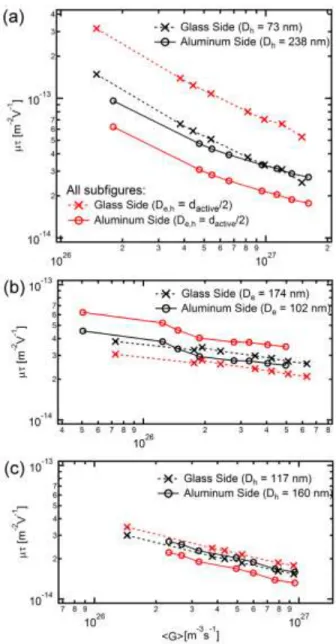
Copy Right 2012, WILEY-VCH Verlag GmbH & Co. KGaA, Weinheim. ... 29 Figure 2.9 Average distance holes are created from the anode, Dh,as dictated
by the local absorption profile for (a) P3HT:PC60BM, (b) MDMO-PPV:PC60BM,
and (c) PCDTBT:PC60BM solar cells with dactive = 310 nm, 280 nm, and 270 nm,
respectively. Dashed lines indicate Dh for constant G, where Dh= dactive/2.
Reprinted with permission from Ref. 56 Copy Right 2012,
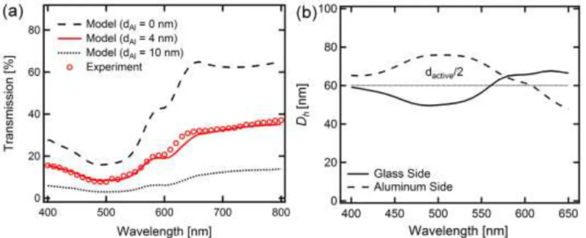
WILEY-VCH Verlag GmbH & Co. KGaA, Weinheim. ... 32 Figure 2.10 (a) Device transmission and (b) Dh for P3HT:PCBM device with
dactive = 120 nm. As with the thicker dactive = 310 nm device the transmission is
very sensitive to dAl. In terms of Dh, there is a less significant difference between
glass and Al side illumination compared to the thicker device. Due to the minimal bimolecular recombination measured for this device for both illumination sides, it is concluded that the Dh and De values are less than those required to instigate
bimolecular recombination for this sample. Reprinted with permission from
Ref. 56. Copy Right 2012, WILEY-VCH Verlag GmbH & Co. KGaA, Weinheim. ... 33 Figure 2.11 Photocurrent (Jphoto = Jlight – Jdark) under various light intensities
when illuminating with λ = 473 nm from (a,c,e) glass side and (b,d,f) Al side for devices with (a,b) P3HT:PC60BM, (c,d) MDMO-PPV:PC60BM, and (e,f)
PCDTBT:PC60BM as the photoactive layer. Model lines are fits to the Hecht
equation where the mobility lifetime product is determined as shown in Figure 2.13. Reprinted with permission from Ref. 56. Copy Right 2012,
WILEY-VCH Verlag GmbH & Co. KGaA, Weinheim. ... 35 Figure 2.12 Scaling exponent of photocurrent with light intensity for
(a) dactive = 120 nm and 310 nm P3HT:PC60BM, (b) dactive = 280 nm
MDMO-PPV:PC60BM, and (c) dactive = 270 nm PCDTBT:PC60BM devices.
Reprinted with permission from Ref. 56. Copy Right 2012,
Figure 2.13 Mobility-lifetime product of restricted carrier species,
μτ, as a function of average exciton generation rate as determined from fits to the Hecht equation to photocurrent data from Fig. 2.11. When using
De or Dh in Equation 4 depending on whether the restricted carriers are
electrons or holes, respectively (as deduced from Fig. 2.12), similar
values of μτ are obtained for glass and Al side illumination (black data points). On the other hand, setting De,h= dactive /2 in Eq. 4, as is the case for
a uniform local absorption profile, causes disagreement in μτ (red data points). Lines are guides to the eye. Reprinted with permission from Ref. 56.
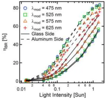
Copy Right 2012, WILEY-VCH Verlag GmbH & Co. KGaA, Weinheim. ... 41 Figure 2.14 Bimolecular recombination efficiency (ηBR) under solar simulated
light bias (glass side) when simultaneously illuminating a monochromatic modulated light (λmod) from either the glass or Al side of the device. Data
corresponds to P3HT:PC60BM device with dactive = 310 nm. The largest
recombination is noted for shorter λmod with Al side illumination (i.e. long Dh)
while the least recombination occurs for glass illumination with shorter λmod
(i.e. short Dh). Lines are included to guide the eye. Reprinted with permission
from Ref. 56. Copy Right 2012, WILEY-VCH Verlag GmbH & Co. KGaA,
Weinheim. ... 43 Figure 2.15 Photocurrent under various light intensities for P3HT:PCBM
device with dactive = 310 nm when illuminating under the following wavelengths
and illumination directions: (a) λ = 473 nm, glass side; (b) λ = 473 nm, aluminum side; (c) λ = 633 nm, glass side; (d) λ = 633 nm, aluminum side. There are significant differences in the photocurrent when illuminating with λ = 473 nm due to drastic differences in De,h depending on illumination
side. For λ = 633 nm, the photocurrent is almost identical due to
De,h≈dactive/2 = 155 nm. Reprinted with permission from Ref. 56.
Copy Right 2012, WILEY-VCH Verlag GmbH & Co. KGaA, Weinheim. ... 44 Figure 2.16 Calculated ratio of dactive/2 to Dh for 1 Sun illumination as a function
of dactive for the three BHJ blends studied herein. Greater deviation from unity
as dactive increases indicates a local absorption profile becoming less uniform
and more weighted toward the PEDOT:PSS / BHJ interface in the photoactive layer. Reprinted with permission from Ref. 56. Copy Right 2012,
WILEY-VCH Verlag GmbH & Co. KGaA, Weinheim. ... 46 Figure 2.17 Diagram of transient photocurrent experimental set up. The device can illuminated from either side by a pulsed laser. ... 51 Figure 2.18 Transient photoconductance (I/Vint) vs time measured under
different Vapp. VBI is estimated from Voc to be 0.5V. ... 52
Figure 2.19 Simulated transient response with illumination from both either side of the device. a) conventional device and b) inverted device.
xiii
ITO/PEDOT:PSS/P3HT:PC60BM/Al (conventional) and
ITO/ZnO:Al/P3HT:PC60BM/WO3/Al (inverted). ... 54
Figure 2.20 Measured transient response with illumination from both
either side of the device. a) conventional (ITO/PEDOT:PSS/P3HT:PC60BM/Al)
device and b) inverted device (ITO/ZnO:Al/P3HT:PC60BM/WO3/Al). ... 55
Figure 2.21 Estimated sweep-out time of the faster carrier (i.e. electron) vs. the inverse of the internal voltage in both cases of metal and glass side illumination. In sweep-out limit (high internal voltage), the mobility
may be extracted from a linear fit of the data according to the drift equation tsw= d
De/µeVint ... 57
Figure 2.22 Transient current under forward bias (Vapp >0 ) in both cases of metal
and glass side illumination. The lifetime can be estimate from the time
of signal decay to 1/e. ... 57 Figure 2.23 Simulated transient photocurrent with different sets of electron/hole
mobilities... 58 Figure 2.24 Transient photocurrents under bias of Vapp= -2 V with illumination from
metal and glass sides. ... 58 Figure 3.1 Schematic procedure of nanoimprinted OPV devices fabrication:
1. spin-coating SU-8 on glass substrate. 2. Emboss SU-8 by PFPE mold to form nanostructures. 3 Deposit ITO thin film on top of nanoimprinted SU-8 by PLD. 4. Evaporate WO3 layer. 5. Spin-coat active materials and evaporate Ca/Al as
electrode to complete the device. Reprinted with permission from Ref. 129.
Copy Right 2013, IOP... 62 Figure 3.2 SEM image of patterned SU-8 coated with ITO/WO3 prior to spin-coating
active materials. Reprinted with permission from Ref. 129. Copy Right 2013, IOP. ... 63 Figure 3.3 Cross-sectional SEM image of nanostructured OPV device. (a)
Whole view of the cross-section. (b) Detail image of device configuration.
Reprinted with permission from Ref. 129. Copy Right 2013, IOP. ... 66 Figure 3.4 All OPV cell’s Jsc (a ~ c) (solid squares are flat cells and open
squares are patterned cells) and efficiencies (d ~ f) (solid triangles are flat cells and open triangles are patterned cells). Under certain fabrication condition, patterned device showed better performance, however no global enhancement
Reprinted with permission from Ref. 129. Copy Right 2013, IOP. ... 67 Figure 3.5 Experimental and simulated angular reflections of the patterned device
with 12 nm WO3 and spun at 800 RPM. Solid lines are experimental
larger uncertainty in the P3HT absorption constants tail beyond this point.122
Reprinted with permission from Ref. 129. Copy Right 2013, IOP. ... 70 Figure 3.6 Angular Reflections and IPCEs in both p and s polarization of the flat
and patterned devices with 12 nm WO3 and spun at 800 RPM. (a) and (b) are the
patterned devices. (c) and (d) are the flat devices. Local IPCE enhancements are indicated by arrows. Reprinted with permission from Ref. 129.
Copy Right 2013, IOP... 71 Figure 3.7 Experimental (a ~ c) and simulated (d ~ e)reflections from the glass
sides of both the flat and patterned devices with 12 nm WO3. Solid lines are
flat samples’ reflections. Dashed lines are patterned samples’ reflections.
Reprinted with permission from Ref. 129. Copy Right 2013, IOP. ... 73 Figure 3.8 IPCEs from glass sides of both the flat and patterned devices
with 12 nm WO3. Solid lines are flat samples’ IPCEs. Dashed lines are
patterned samples’ IPCEs. Reprinted with permission from Ref. 129.
Copy Right 2013, IOP... 73 Figure 3.9 SCLC measurement for hole mobility measurement. Solid lines are
fittings to equations to obtain estimation of hole mobility. The averaged patterned device thickness is estimated from pattern geometry.
Reprinted with permission from Ref. 129. Copy Right 2013, IOP. ... 75 Figure 3.10 Logarithm to base 10 of the electric field strength [V m–1] at
maximum power in two bulk heterojunction solar cell devices with ridge-patterned front electrodes. The devices are closed by a glass layer in the front and by an aluminum layer in the back. Length units are nanometers. The electric field is weaker in the ridge part because of the larger distance between the electrodes. The induced losses may outweigh the gain in light absorption achieved
by the photonic crystal structure. Reprinted with permission from Ref. 129.
Copy Right 2013, IOP... 76 Figure 3.11 Current density [A m-2] at maximum power in the two patterned
solar cell devices (a) and (b). The current density is low in regions of the deeper ridge pattern, which deteriorates the charge transport properties of device (a).
Reprinted with permission from Ref. 129. Copy Right 2013, IOP. ... 77 Figure 3.12 Sketch of the inverted and conventional grating structures:
(a) In an inverted device, electrons are collected in the front electrode after being selected by the electron transport layer (ETL) and holes are collected in the back electrode after being selected by the hole transport layer (HTL) in the inverted device (b) The opposite charge transport direction define
the conventional structure. Dimensions W,T, H and P were varied numerically. Reprinted with permission from Ref. 126. Copy Right 2013, American Institute of
xv
Figure 3.13 Simulated current density vs. applied electric potential characteristics for best performing PTB7:PC70BM (flat and patterned) devices. Reprinted with
permission from Ref. 126. Copy Right 2013, American Institute of Physics. ... 81 Figure 3.14 Absorption vs. effective thickness (a) and efficiency vs. effective
thickness (b) of both inverted (ITO/PFN/PTB7:PC70BM/WO3/Ag) and
conventional (ITO/PEDOT:PSS/PTB7:PC70BM/Ca/Ag) devices in the
flat and patterned structures. Reprinted with permission from
Ref. 126. Copy Right 2013, American Institute of Physics. ... 82 Figure 3.15 Efficiency plots: The flat and patterned PTB7 devices’ output power
to absorbed power vs. absorbed power to input power. The product of these two values is the efficiency of one device. Intersection of the dash
lines marks the best flat device. Region I: both electrical and optical enhancements. Region II: Electrical enhancement but optical deterioration. Region III:
both electrical and optical deteriorations. Region IV: optical enhancement but electrical deterioration. Reprinted with permission from Ref. 126.
Copy Right 2013, American Institute of Physics... 84 Figure 3.16 Efficiency plots of P3HT:PC60BM devices. Reprinted with
permission from Ref. 126. Copy Right 2013, American Institute of Physics. ... 84 Figure 3.17 The ratios of absorbed power of the patterned devices to that
of the flat devices with the same volumes (blue) and the ratios of carrier collection efficiency to that of the flat devices with the same volumes (red). Reprinted with permission from Ref. 126.
Copy Right 2013, American Institute of Physics... 86 Figure 3.18 Product of the ratios shown in Fig 3.17. Reprinted with
permission from Ref. 126. Copy Right 2013, American Institute of Physics. ... 86 Figure 3.19 The ratios of absorbed power of patterned devices to that of the best flat device and the ratios of carrier collection efficiency to that of the best flat device. Reprinted with permission from Ref. 126. Copy Right 2013, American Institute of
Physics. ... 87 Figure 3.20 Absorbed power of the 400 patterned inverted
(ITO / PFN / PTB7:PC70BM / WO3 / Ag ) and conventional
(ITO / WO3 / PTB7:PC70BM / PFN/Ag) structures studied.
Reprinted with permission from Ref. 126. Copy Right 2013, American Institute of
Physics. ... 88 Figure 3.21 Electron-hole pair generation density (m-3s-1) profile of active layers
in one inverted device (a) (ITO/PFN/PTB7:PC70BM/WO3/Ag) and
one conventional device (b) (ITO/WO3/PTB7:PC70BM/PFN/Ag).
Reprinted with permission from Ref. 126. Copy Right 2013, American Institute of
Figure 3.22 Log10 of the electric field (V m-1) profile of the inverted (a)
and conventional (b) devices shown in Figure 3.22. Reprinted with permission
from Ref. 126. Copy Right 2013, American Institute of Physics. ... 89 Figure 3.23 Simulations of patterned inverted devices
(ITO/PFN/PTB7:PC70BM/WO3/Ag) and conventional devices
(ITO/WO3/PTB7:PC70BM/PFN/Ag). Black Solid and dash lines are the flat inverted
and conventional devices respectively. Red round dots are the patterned inverted devices and violet triangle dots are the patterned conventional devices. a) electron mobility is greater (μn = 5.8×10⁻⁷ m2/V s, μp = 1.7 ×10⁻⁷ m2/V s). b) hole mobility is
greater (μn = 1.7×10⁻⁷ m2/V s, μp = 5.8 ×10⁻⁷ m2/V s). c) electron and hole moblities
are equal (μn = 1.7×10⁻⁷ m2/V s, μp = 1.7 ×10⁻⁷ m2/V s). Reprinted with permission
from Ref. 126. Copy Right 2013, American Institute of Physics. ... 90 Figure 3.24 Electron (left) and hole (right) flux (m-2s-1) (a) inverted devices (b)
conventional devices when electron mobility are greater than the hole mobility (μn = 5.8×10⁻⁷ m2/V s, μp = 1.7 ×10⁻⁷ m2/V s). Reprinted with permission from
Ref. 126. Copy Right 2013, American Institute of Physics. ... 92 Figure 3.25 Electron and hole flux (m-2s-1) (a) inverted (b) conventional when the
hole’s mobility are greater than the electron’s (μn = 1.7 ×10⁻⁷ m2/V s,
μp = 5.8×10⁻⁷ m2/V s). Reprinted with permission from Ref. 126.
Copy Right 2013, American Institute of Physics... 92 Figure 3.26 Simulations of the inverted devices (ITO/PFN/PTB7:PC70BM/WO3/Ag)
and conventional (ITO/WO3/PTB7:PC70BM/PFN/Ag). Black solid and dash lines are
the flat inverted and conventional devices respectively. Red dots are the patterned inverted devices and violet dots are the patterned conventional devices. a) Electron mobility is one order of magnitude greater than hole mobility μn = 1.7×10⁻⁷ m2/V s,
μp = 1.7×10⁻⁸ m2/V s) b) Hole mobility is one order of magnitude greater than
electron mobility ( μn = 1.7×10⁻⁸ m2/V s, μp = 1.7×10⁻⁷ m2/V s).
Reprinted with permission from Ref. 126. Copy Right 2013, American Institute of
Physics. ... 94 Figure 3.27 (a) SEM and (b) AFM images of patterned RReg P3HT:PCBM
photoactive layer. The patterns are comprised of posts spaced by 400 nm in a hexagonal array with 200 nm diameters. Adjacent posts are connected by a residual flash layer as shown in (c) where P3HT polymer chains are green and PCBM
molecules are black spheres (not to scale). ... 96 Figure 3.28 (a) Absorbance of photoactive nanopattern for 284.4 eV incident photon energy taken with STXM. Within the image area, a region without nanopattern is used to simultaneously measure the incident photon flux, I0.
(b) Masks that isolate posts (left) and flash (right) are used to determine
xvii
Figure 3.29 Measured absorbance and composition fits for (a) post areas and (b) exposed flash layer for nanopatterns imprinted at different temperatures. Absorbance for each energy corresponds to a separate image using the masking technique described in Fig. 3.27. For all temperatures, there is higher PC60BM
percentage by weight in the posts than in the flash layer as labeled. This leads to flash layer composition that is below the optimum for high performance.
The spectra for 140º and 25 °C are vertically offset for clarity. Pure material NEXAFS reference spectra for P3HT and PC60BM with unique spectral
fingerprints are also shown in (b). ... 100 Figure 3.30 (a,b) Thickness and (c,d) composition maps derived from STXM
measurements of nanopatterns comprised of PC60BM and (a,c) RReg P3HT
and (b,d) RRan P3HT. Both nanopatterns are fabricated at 140 ºC. The composition differences between the posts and the flash layer are minimal in the nanopattern made with amorphous RRan P3HT compared to the nanopattern made with
semicrystalline RReg P3HT. ... 102 Figure 3.31 GIWAXS scattering data for (a) non-patterned, planar
RReg P3HT:PC60BM and RReg P3HT:PC60BM nanopatterned samples,
with the important peaks labeled. (b) In plane and out of plane sector averages reveal that nanoimprinting causes P3HT crystals to become more face-on with respect to the substrate compared to the non-patterned planar film. Sector averages are also shown for the RRan P3HT:PC60BM nanopatterned
sample that lacks crystal reflections. It should be noted that (a) are not corrected
LIST OF SYMBOLS AND ABBREVIATIONS
a electron-hole pair distance
AFM atomic force microscope (microscopy)
APCE absorbed photon-to-electron conversion efficiency
Ag silver
Al aluminum
Au gold
BHJ bulk heterojunction Cu2O Copper (I) oxide
d layer thickness
De electron transport distance
Dh hole transport distance
Eg band gap
EQE external quantum efficiency
IPCE incident photon-to-electron conversion efficiency
FF fill factor
G exciton (electron-hole pair) generation rate GIWAXS grazing incidence wide angle X-ray scattering HOMO highest occupied molecular orbital
HTL hole transport layer
IQE internal quantum efficiency ITO indium tin oxide
Jdark dark current
Jlight light current
Jn(p) electron or hole current
Jphoto photocurrent density
xix
Jsat saturated photocurrent density
Jsc Short circuit current density
k extinction coefficient
kB Boltzmann constant
L diffusion length
LUMO lowest unoccupied molecular orbital
MDMO-PPV poly(2-methoxy-5-(3’-7’-dimethyloctyloxy)-1,4-phenylenevinylene
n electron density
NEXAFS near edge X-ray absorption fine structure NIL nanoimprint lithography
OPV organic photovoltaic
p hole density
P probability of electron-hole pair dissociation P3HT poly(3-hexylthiophene)
PBHJ parallel bulk heterojunction PbS lead (II) sulfate
PC photonic crystal
PC60BM phenyl-C61-butyric acid methyl ester
PC70BM phenyl-C71-butyric acid methyl ester
PCDTBT poly((9-(1-octylnonyl)-9H-carbazole-2,7-diyl)-2,5-thiophenediyl-2,1,3-benzothiadiazole-4,7-diyl-2,5-thiophenediyl)
PCE power conversion efficiency
PEDOT:PSS poly(3,4-ethylenedioxythiophene):poly(styrenesulfonate)
PFN poly [(9,9-bis(3´-(N,N-dimethylamino) propyl)-2,7-fluorene)-alt-2,7-(9,9– dioctylfluorene)]
PFPE perfluoropolyether PLD pulsed laser deposition
PTB7 Poly[[4,8-bis[(2-ethylhexyl)oxy]benzo[1,2-b:4,5-b']dithiophene-2,6-diyl][3-fluoro-2-[(2-ethylhexyl)carbonyl]thieno[3,4-b]thiophenediyl]] PV photovoltaic
q elementary charge
R Recombination Rate
Rsh shunt resistance
Rs series resistance
SCLC space charge limited current SEM scanning electron microscopy
STXM scanning transmission x-ray microscopy
T absolute temperature
TCO transparent conducting oxide
tR recombination time
tsw sweep-out time
U net generation rate
V Voltage
V0 the applied voltage at Jphoto = 0
Vapp applied voltage
Vmp voltage at maxim power point
Voc open circuit voltage
x depth
XRD X-ray diffraction
w depletion width WO3 tungsten trioxide
α monochromatic absorption coefficient
λ wavelength
xxi
μ mobility
τ lifetime
φ the flux of incident photons
CHAPTER 1
INTRODUCTION
1.1 Motivation: World’s Energy Needs
Fossil gas and oil currently constitute our principal sources of energy worldwide. Their rising costs and finite abundance have driven interest in renewable alternatives since the 1970s. Despite recent development in shell gas extraction, the interest in alternative energy has kept growing as the emissions of burning fossil fuels such as carbon dioxide and other green-house gases have been extensively associated with a large number of undesirable environmental and climatic consequences. Taking all new developments and policies into account, the world is clearly failing to put the global energy system onto a sustainable path.1 The search for alternative energy sources is more pressing than ever.
2
theoretical limit of efficiency would not provide the needed technology unless it is cost-effective.3 This conundrum has led to research not only on improvements in efficiencies of current solar cells, but also on alternative photovoltaic material and thin film technologies that seek to reduce the cost of solar cells production and installation. Promising photovoltaic inorganic compounds, such as copper (I) oxide (Cu2O) and lead
(II) sulfate (PbS), were proposed to meet the cost-effective requirement based on their electricity production potential and minimum cost per watt of electricity.4 Another avenue to lower the cost of photovoltaic devices is the development of semiconducting and conducting organic polymers that can be processed from solution, hence the possibility of simple roll-to-roll printing processes, leading to inexpensive, large scale production.3,5 In addition, the organic photovoltaic (OPV) could be beneficial for the applications where mechanical flexibility and disposability are important.3
In this thesis, the discussion will focus on the charge transport issues and device architectures in two types of the promising photovoltaic systems: Cu2O and organic
photovoltaics. It is organized in the following way: in the rest of this chapter, we will discuss the progress of Cu2O and organic photovoltaic devices, fundamental physics and
1.2 Potential Novel Photovoltaic Materials
1.2.1 Copper (I) oxide (Cu2O)
In recent years, the need for sustainable energy technologies with increasing emphasis placed on balancing cost and performance invigorated a renewal of interest in solar cells based on copper (I) oxide (Cu2O) as the active layer because this semiconductor shows
many important characteristics useful for solar cells production. These include low raw material cost, a direct energy gap (~2.1eV), nontoxicity, long term stability, and it is amenable to low cost scalable fabrication process such as electrodeposition.6 However, the fundamental limitations of Cu2O, one of the earliest semiconductors to be studied,
have not been overcome. In particular, the difficulty of fabricating n-type Cu2O,
homojunctions remains a barrier to the realization of Cu2O based solar cells. More
recently transparent conducting oxide (TCO)/Cu2O heterojunction solar cells have been
pursued, especially the ZnO/Cu2O solar cells. Although the theoretical limit of the power
conversion efficiency of Cu2O based solar cell is about 18%,7 the highest efficiency of
ZnO/Cu2O device reported is 1.28%.6 An inadequate minority carrier transport length has
been implicated as an important factor behind this poor performance.8–10
1.2.2 Organic Photovoltaic Device
4
acceptor materials in solution. This revolutionary idea circumvented the short exaction (electron and hole pair) diffusion length with distributed donor/acceptor interfaces throughout the BHJ layer.12,13 Moreover, it allows solution processing of active layer instead of thermal evaporation under vacuum, which makes mass productions much cheaper. These results jumpstarted expansive research and inspired the possibility of making solar cells using simple processing techniques from plastic, lightweight, and flexible materials. By 2005, with the development of materials and processing techniques, the PCE had risen to 4.4%, using an electron donor polymer, poly-3-hexylthiophene (P3HT), and electron acceptor molecule, phenyl-C61-butyric acid methyl ester (PC60BM).14 Today, this material system are the most studied and well-understood BHJ
solar cell system. But, device performance did not stop there as efficiency has been improved to > 9% by 2012.15 Besides the fast development of OPV materials, characterizations of the photon absorption, free charge generation and charge carrier collection process have also drawn great attentions.16–20 These boost development of the characterization techniques to study new materials emerging and guide material engineering towards desired features to reach high efficiencies as well.
1.3 Light Absorption and charge generation in Solar Cells
Semiconductors are characterized by a band gap, Eg. Eg is the difference between
be absorbed when light hitting the material thereby promoting electrons from valence band to conduction band or from HOMO to LUMO. Excited electron will relax either non-radioactively or by emitting a photon with energy of Eg. An electric field or gradient
in carrier concentration will help to extract the current in the device.
Formally, the complex index of refraction is denoted by nˆ n ik, where n is the
refraction index and k is the extinction coefficient. The absorption coefficient at a given
wavelength λ of the material is abs 4
k
. k will be zero at wavelengths where the
energy above Egand hence the αabs is zero there. For a single thick absorbing material like
Cu2O, the profile of absorption of photons or generation rate of excitons follows a
function of the depth (x) in the film which is given by ( )G x (1R)ex, where is
6
Figure 1.1 Example of light absorption/charge generation profile of a 112 nm thick P3HT:PC60BM blend layer in a working device with full electrodes.
After a photon is absorbed, an excited state is generated, which is an electron and hole pair. In most of the inorganic solar cells, such as Si and Cu2O,22 this electron and
hole pair or exciton breaks by the thermal vibration because its binding energy is usually small compared to kBT at room temperature, where kB is Boltzman constant and T is
absolute temperature. Therefore, after absorption, free carrier is generated. Cu2O is a
p-type semiconductor where the hole is dominant and easy to move. Hence, the charge collection mainly depends on the minority carrier, the electron.
The situation is more complicated in BHJ OPVs. The exciton’s binding energy is large compared to kBT. The electron and hole pair will not break right away. There are
different models that exist to explain the free carrier generation and collection in BHJ OPV devices. One of the most established and well accepted models is presented by Koster et al. in 2005.21 The model describes the OPV device by the metal-insulator-metal
absorbed, an exiton is created. The exciton dissociates across the donor-acceptor interface and yields a bound electron-hole pair. The dissociation of this bound electron-hole pair generates free charge carriers. The dissociation of exciton is driven by the difference between the LUMO levels of the two materials, which is assumed to be field independent, while the bounded electron-hole pair’s dissociation is considered as field and temperature dependent because it is metastable ( up to milliseconds at 80 K ).21
In Koster’s model,21 the generation of free carriers was explained by geminate recombination theory of Onsager23 with the refinement by Braun24. The bound electron-hole pair may dissociate into free carriers or decay to the ground state with a decay rate
kf. And the dissociation with a rate kdiss is competing with recombination rate R. In
Braun’s model, the probability of electron-hole pair dissociation is given by
( , , ) ( , , )
( , , ) ( ) diss
diss f
k a T F P a T F
k a T F k T
, where a is electron-hole pair distance and F is electric
field strength. The recombination is considered as bimolecular recombination and with
rate 2
int
( )
R np n . γ is the recombination strength and nint Ncexp(Egap/ 2 )Vt , where
Vt=kBT/q and q is the elementary charge. The whole progress from absorption of photons
8
Figure 1.2 Progress from absorption of photons to generation of free carriers. Upon absorption, excitons are created and diffuse to the donor/acceptor interface where the electrons are transferred to the acceptor and bound electron-hole pairs are formed. The bound pair may either dissociate and become free carriers or decay to the ground state. The dissociation also competes with recombination.21
interface in 100 fs. This is in contrast with the previous picture of bound excition formation upon photon absorption. Heeger group then proposed an alternative picture of free carrier generation that the delocalized and/or mobile electrons and holes are formed directly in the conduction and valence bands after the interband absorption rather than the relaxed excitons which are localized by structural relaxation of the polymer and bound by the Coulomb interaction. Hence, the primary excitation can reach the interface faster than an exciton, which could account for the ultrafast charge separation. The charge separation does not rely on electric field or other thermal vibration because there is excess energy in the system. Therefore, they suggested it is very possible that charge transfer from the polymer to the fullerene directly yields free charge carriers. Recombination in BHJ solar cells should be bimolecular or trap-based, instead of geminate.
1.4 Equations of Charge Carrier Collection
After the exciton or electron-hole pair separates, excess charges are created in the polymer and fullerene domains due to photoexcitation and subsequent charge transfer, as discussed in the previous section. Mobile (free) carriers must then be generated and collected at opposite electrodes prior to recombination. Despite the argument of free carrier generation, the free carrier collection process can be described by basic equations below:
2
2 ( ) [ ( ) ( )]
q
x n x p x x
(1.1)
10
( ) ( ) n
J x qU x x
(1.2)
( ) ( )
p
J x qU x x
(1.3)
where Jn(p)(x) is the electron (hole) current density and U(x) is the net generation rate, i.e.,
the difference between generation of free carriers and recombination of free carriers.
In order to solve those basic equations, a set of equations is needed to relate the current densities to the carrier densities and the potential. Incorporating both drift and diffusion of charge carriers, one has
n n n
J qn qD n
x x
(1.4)
p p p
J qn qD p
x x
(1.5)
where Dn,p are the carrier diffusion coefficients, which are assumed to obey the
Einstein relation21
, , /
n p n p B
D k T q (1.6)
1.5 Basic Characterization of Solar Cell Devices
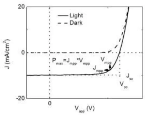
1.5.1 J-V measurement and Power Conversion Efficiency
When a solar cell is illuminated with light and placed under short-circuit (i.e. applied voltage (Vapp) = 0 V), photocurrent is produced in the external circuit. This point is
labeled as the short-circuit current (Jsc) on the standard current density vs. voltage (J-V)
applying negative bias across the device that raises the internal electric field strength. If the current under illumination (Jlight) is subtracted from the current in the dark (Jdark), then
this amount, the photocurrent (Jphoto), will saturate to a level proportional to the amount
of light absorbed in the BHJ layer. As Vapp is increased to positive bias, then the
extraction of carriers decreases in part due to a decrease in the internal field, but also due to increased injection of holes from the anode and electrons from the cathode (i.e. Jdark).
Under open-circuit conditions, the internal field is very weak and Jlight = 0. With even
more application of bias, the current increases rapidly until it becomes linear with a slope controlled by the series resistance (Rsr) of the device. The power conversion efficiency
(PCE) of the solar cell is calculated as
1
PCE= sc oc
sun
J V FF
I
(1.7)
where the AM 1.5 solar power 1 sun=100 mW/cm2 and FF is fill factor which is defined as,
MPP MPP sc oc
J V
FF
J V
(1.8)
12
Figure 1.3 J-V under dark and illumination of one solar cell device.
1.5.2 Quantum Efficiencies
A solar cell's quantum efficiency (QE) value indicates the amount of current that the cell will produce when irradiated by photons of a particular wavelength. If the cell's quantum efficiency is integrated over the whole solar electromagnetic spectrum, one can evaluate the amount of current that the cell will produce when exposed to sunlight. The ratio between this energy-production value and the highest possible energy-production value for the cell (i.e., if the QE were 100% over the whole spectrum) gives the cell's overall energy conversion efficiency value. Note that in the event of multiple exciton generation, quantum efficiencies of greater than 100% may be achieved since the incident photons have more than twice the band gap energy and can create two or more electron-hole pairs per incident photon.
photons of a given energy shining on the solar cell from outside (incident photons). It is defined as
/ sec / sec
photo
light
J
electrons h EQE
photons P q c
(1.9)
where Plight is incident light intensity, h is plank constant and c is light speed.
Internal Quantum Efficiency (IQE, also known as Absorbed photon-to-electron conversion efficiency, APCE) is the ratio of the number of charge carriers collected by the solar cell to the number of photons of a given energy that shine on the solar cell and are absorbed by the cell. The IQE is always larger than the EQE. A low IQE indicates that the active layer of the solar cell is unable to make good use of the photons. To measure the IQE, one first measures the EQE of the solar device, then measures its transmission and reflection, and combines these data to infer the IQE.
1.6 Active Layer Thickness: A Trade-off
14
low fabrication costs, the dilemma is remarkably similar. They are strong light absorbers, capable of almost total light-absorption with a thin 200 nm layer, but their carrier mean free paths are considerably shorter. The resulting efficiency is reportedly still too low to be practical.
1.7 Nanostructure and Application
Nanostructure has been frequently applied to solve the problem that lies in the incompatible lengths scale of optical absorption and charge carrier collection.9,10,42–50 For instance, Musselman et al. proposed ZnO nanowires to reduce the charge carrier transport distance in ZnO/Cu2O solar cells.9,10 Some of the others seek for optical improvement.
towards nanostructures in photovoltaic devices and it will focus on the application of photonic crystal structures in OPVs.
1.8 Importance of Transport
There are two important distances in photovoltaic materials: charge carrier transport length and the charge carrier transport distance. The former length is the capability of the carriers to transport across the material. The latter is the distance that the charge carrier needs to travel to be collected. The charge carrier transport remains critical factor which determines the solar cells’ efficiency, even though the nanostructures can increase the
total light absorption or reduce the charge carrier transport distance. Characterization of transport length helps the design of nanostructure to achieve the efficiency enhancement. For instance, the nanowires can reduce the electron transport distance.10 But, if a nanostructure scale less than this critical length, it will not bring additional benefits and could have a detrimental effect given the numerous potential interface defects that scale as the heterojuntion contact area increases, in itself a big concern responsible for the less than expected Voc. Additionally, in nanostructured OPV devices, the changes of electric
CHAPTER 2
CHARACTERIZE CHARGE CARRIER TRANSPORT BY
MANIPULATING ABSORPTION PROFILE
2.1 Introduction
beyond the transport length, they are not able to be collected by electrodes. Therefore, the transport length is obliviously the factor limiting thickness of the planar active layer. In addition, the photonic crystal solar cell should be designed mindful of charge carrier transport as mentioned previously. In this thesis, minority carrier transport length in Cu2O
was probed by this method.8 A nanostructure scale less than the critical length will not bring additional benefits and could have a detrimental effect given the numerous potential interface defects that scale as the heterojunction contact area increases. In the case of BHJ OPVs, a similar method was applied to reveal the relation between charge generation profile and the recombination mechanism, an important process during charge carrier transport. The product of mobility and lifetime of the carrier was estimated.56 This technique were used in transient photocurrent measurements and we revealed the physical process of electron and hole transport and demonstrated the potential of measuring mobility and lifetime.
2.2 Minority Carrier Transport Length in Cu2O/ZnO Solar Cell
To estimate the minority carrier (i.e electron) transport length in Cu2O, the Cu2O/ZnO
device was made. ZnO film on glass substrate was prepared by pulsed laser deposition (PLD) using 99.99% purity ZnO target. To get good conductivity ZnO film with a surface receptive to Cu2O to growth, two layers of ZnO was deposited sequently under different
conditions. A ZnO layer ~200 nm thick is deposited on glass substrate at 200 oC with 10 mTorr O2 and it is followed by ZnO of ~500 nm deposited at room temperature under
200 mTorr O2. The Cu2O layer was electrodeposited in an aqueous solution onto
18
The electrodeposition is performed with a current density of -0.9 mA/cm2 at 40 oC. A total electric charge of 2 C/cm2 corresponds to the film thickness of ~1.6 μm. To complete the device, a semitransparent gold layer of ~20 nm was sputtered on Cu2O as
anode contact. The whole device was later annealed on for 1 hr at 200 oC.
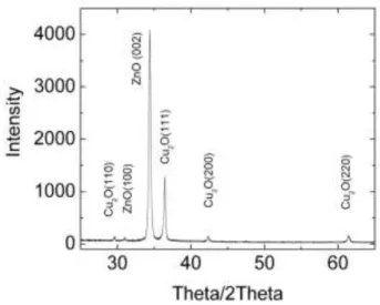
Figure 2.1 X-Ray diffraction of the ZnO/Cu2O solar cell.
Fig. 2.1 shows X-Ray diffraction measurements which confirm only Cu2O is formed
on the ZnO without trace of CuO. A scanning electron micrograph (SEM) of the cross section of the device is shown in Fig 2 where the thickness of each layer of the device is assessed. In Figure 2.3, the solar cell has been also characterized by J-V scan, both in dark and under AM 1.5 conditions (front illumination). From where, Jsc = 3.16 mA/cm2
and a Voc = 0.11V are measured. The efficiency is low because of the thin gold electrode
which reduced the light absorption and increased the series resistance. Fig. 2.3 shows the IPCE measurements with illumination from both back and front of the cell. The Jsc of
Figure 2.2 Cross-sectional SEM (45° tilt) of the ZnO/Cu2O solar cell. Inset: schematic of the complete device solar cell and electron generation profiles for front and back illumination. Reprinted with permission from Ref. 8. Copy Right 2011, American Institute of Physics.
Figure 2.3 IPCE measurements with illumination from both sides. Solid circle is glass side illumination while solid square is from gold side. Inset is J-V measurement under dark and AM 1.5 conditions. Dash line is dark current and solid line is light current. Adapted with permission from Ref. 8. Copy Right 2011, American Institute of Physics.
Previously studies22,57 estimated the electron diffusion length in Cu2O ranging from 2
to 12μm using Gärtner’s model58
20
in these devices. To probe the transport length in electrodeposited Cu2O, we have
modified Gärtner’s model following the work of Södergren et al.59
All of the parameters are obtained from the IPCE measurements and known optical constants.
As shown in Gärtner’s model, 58
the photo current is given by,
DL DIFF
J J J (2.1)
where JDL is the drift current density due to carriers generated inside the depletion layer,
and JDIFF is the diffusion current density of minority carriers generated outside the
depletion layer in the bulk of Cu2O and diffusing into the depletion region.
0 ( )
w DL
J q
G x dx (2.2)where w is width of depletion layer, x = 0 is at the interface of ZnO and Cu2O and q is
element charge. JDIFF is determined by Eq. (2.2) for the excess concentration of electrons
n(z) .
2
0 2
0
( ) ( )
( ) 0
n x n x
D G x
x
(2.3)
The boundary conditions are n(w) = 0 and corresponding to a total carrier sweep and negligible electron current toward the anode, respectively.60 d is the thickness of Cu2O
layer. This last condition is used instead of Gärtner’s n(∞) = 0 which is only appropriate
for a bulk semiconductor and is not adequate for thin electrodeposited devices.
As discussed in previous chapter, Cu2O film is thick and hence G(x) for gold and
( )
( ) d x
Au Au
G x T e (2.4)
/
( ) x
glass glass ZnO
G x T e (2.5)
φ is the flux of incident photons and is α the monochromatic absorption coefficient. Here
TAu and Tglass/ZnO are the transmittance through gold and glass/ZnO to Cu2O, respectively.
They are measured independently by spectroscopic optical transmittance of the individual layers.
Solving Eq. (2.2) with G(x) for back and front illuminations offers the excess electron concentration in the Cu2O film. JDIFF is proportional to the gradient of n(z) at x = w. The
IPCEs (J/φ) for gold and glass sides are given by:
2 2
( ) 2 2
2 2
2 2
2 ( 1 ) (1 )
( 1 )
( )( 1 )
d w dL d
w w
L L L
d
gold d w Au
L L
e L e L e L
IPCE e T
e e L
(2.6) 2 2 ( ) ( ) / 2 2 2 2
e ( 2e e ( 1 ) e (1 ))
(1 e )
(e e )( 1 )
d w Lw w
d d
d w L L L
w
glass d w glass ZnO
L L
L L L L
IPCE T L (2.7)
where L is the diffusion length. For long wavelengths (λ) where α(λ) is small (literature values57) and L1 , one can obtain approximated expressions neglecting those small terms following the work of Lindquist et al.61 A useful feature of this limit is that one can obtain an estimate of the depletion layer width at short circuit conditions:
lass / g glass ZnO IPCE w
d T (at λ where
old
g
Au
IPCE
T is maximum) (2.8)
In our case, the IPCEgold/TAu reaches its maximum at λ =540 nm (Fig. 2.3), where α is
22
from SEM (Fig. 2.2) cross section. L can now be assessed from the ratio of the IPCEgold
to the IPCEglass.
Figure 2.4 Generation profile G(x) (red λ= 500 nm, black λ = 470 nm). Solid lines are glass side illumination. Dashed lines are gold side illumination. Adapted with permission from Ref. 8. Copy Right 2011, American Institute of Physics.
In Fig. 2.5, we plot the both experimental and simulated IPCE ratios. Fig. 2.4 shows
G(x) at 470 nm and 500 nm with illumination for both sides. As we can see, more electrons are generated close to where light enters the Cu2O layer and the generation
increase to the ratio of incident light intensity on Cu2O from the two illumination
directions at long wavelengths. In Fig. 2.5 if L increases, the electron collection becomes more independent on the direction of illumination for all wavelengths, and the ratio of IPCEs is determined mainly by the ratio of transmittances. From Fig. 2.5, L is estimated to be ~ 160 nm. As shown, our model provides a good fit to the IPCE ratio. Therefore, only photogenerated carriers within the distance of L+w (~430 nm) have a faire chance of being collected.
Figure 2.5 Experimental (open triangles) and simulated IPCE ratios with different proposed diffusion lengths (L = 160 nm, 300 nm, 600 nm and 1600 nm). Limit to IPCE ratio is set by the ratio of transmittances of gold to that of glass/ZnO. Adapted with permission from Ref. 8. Copy Right 2011, American Institute of Physics.
The diffusion length found here is significantly shorter at least by one order of magnitude than the values reported previously.5.6 Moreover, when those values are applied with the classical Gärtner’s model to the gold side illumination alone, they resulted in a negative IPCEgold at short wavelengths which is not observed experimentally.
24
IPCE of a Cu/Cu2O solar cell which may have a different, and presumably better,
crystalline structure. Nevertheless, such long L values would be in conflict with the low photocurrents obtained from electrodeposited Cu2O. Furthermore, a qualitative inspection
of the SEM cross section in Fig. 2.2, points to numerous microcrystalline defects that most likely should limit the free scattering path to submicron lengths.
2.3 Charge Transport and Recombination in Organic Photovoltaic Device
2.3.1 Background
The dilemma between light absorption and charge carrier collection is similar in OPVs. Organic polymers are strong light absorbers, capable of almost total light-absorption with a layer of only 200 nm, but their carrier mean free paths are considerably shorter. The resulting efficiency is reportedly still not high enough to be practical. The characterization of charge carrier transport in bulk heterojunction (BHJ) organic solar cells has been a central component to improving the power conversion efficiency (PCE). Using a suite of steady-state and transient techniques, a complex picture of the underlying physical mechanisms leading to photocurrent generation has emerged that has helped guide the design of higher performing materials and devices.62,63 This development has been coincident with empirical evidence refining the optimal processing conditions for the ever-growing number of organic photoactive materials. One such empirical guideline is that the active layer thickness (dactive) must be kept on the order of 100 nm so that
transport distances remains short enough to avoid free carrier recombination. However, this comes at the expense of light absorption efficiency, which generally increases with
Traditionally, the loss of free carriers has been described as non-geminate (recombined electron and hole originate from different excited states) and bimolecular (second order recombination rate that depends on the square of the free carrier density).21 While the loss of free carriers is intuitively non-geminate, bimolecular recombination can only be linked to free carrier loss if it depends on the distances that electrons and holes are required to travel to reach their respective exit contacts. While this has been inferred from comparisons of separate devices where dactive66or carrier mobilities17,67 are varied,
such comparisons may convolve unintentional morphological changes from altered processing conditions. In the recent work,16 it was shown that an indirect link between bimolecular recombination and the distance required for carriers to transit the active layer, but again comparisons were made between different samples with different dactive and
electron/hole transport interlayers. Finally, device models21,68 have also predicted that increasing dactive will lead to greater bimolecular recombination,69 but this effect is to be
expected since free carriers are assumed to be lost only through this process. Establishing a solid experimental basis between bimolecular recombination and carrier transport distances would provide new insight to this loss mechanism that critically influences the open-circuit voltage70,71 and also describes the dark injected current.72
Similarly, as applied to Cu2O solar cell, the characteristic local generation profile in
26
diffusion length) that occurs after exciton diffusion and charge separation at the internal donor/acceptor interfaces. Therefore, G effectively controls the distance carriers must travel in the active layer in order to be extracted, which will later be related to bimolecular recombination losses. We perform this experiment to three polymer/fullerene systems, P3HT, poly(2-methoxy-5-(3’-7’-dimethyloctyloxy)-1,4-phenylenevinylene (MDMO-PPV), and poly((9-(1-octylnonyl)-9H-carbazole-2,7-diyl)-2,5-thiophenediyl-2,1,3-benzothiadiazole-4,7-diyl-2,5-thiophenediyl) (PCDTBT), each blended with PC60BM They cover a broad range of known morphological characteristics (e.g. polymer
crystallinity), quantum efficiency, and device performance.
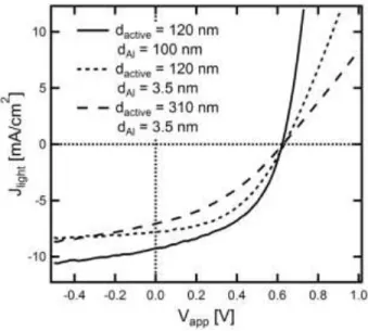
Figure 2.6 Current-voltage characteristics under 1 Sun illumination for P3HT:PC60BM
with thin (dAl = 3.5 nm) and thick (dAl= 100 nm) aluminum cathodes with varying active
layer thickness, dactive. Both the Jsc and FF are reduced due to a marginal drop in light
absorption and increase in serial resistance, respectively, from the use of semi-transparent aluminum electrodes. The Voc remains essentially unchanged. Reprinted with permission
from Ref. 56 Copy Right 2012, WILEY-VCH Verlag GmbH & Co. KGaA, Weinheim.
PCE under 1 Sun illumination comparable to previous reports was obtained for all three polymer/fullerene combinations using the standard device configuration of indium tin oxide (ITO)/poly(3,4-ethylenedioxythiopene):poly(styrenesulfonate) (PEDOT:PSS) / active layer/Al. In order to control the carrier transport distance, semi-transparent cathodes were employed that allow for illumination from either the glass or Al side of the device. Semi-transparent electrodes have been previously demonstrated for BHJ solar cells using non-traditional electrode materials,73–78 but in this work, we incorporate thin layers (~5 nm) of Al. Even with such thin layers, reasonable device performance is achieved with high open-circuit voltage (Voc), where the primary losses originate from a
reduction in light absorption and increase in serial resistance. Each of these result in marginal drops in short-circuit current (Jsc) and fill factor (FF), respectively. Figure 2.6
shows 1 Sun device performance for P3HT:PC60BM devices with dactive = 120 nm and Al
cathode thickness (dAl) of 100 and 3.5 nm. The PCE drops from 2.8% to 2.2% for devices
with dactive = 120 nm and dAl = 100 nm and 3.5 nm, respectively, due to the reductions
mentioned above. Also shown in Fig. 2.6 are device performances for solar cells with
dactive = 310 nm and dAl = 3.5 nm (PCE = 1.6%), where the serial resistance increases
compared to devices with dactive = 120 nm and dAl = 3.5 nm. Use of thicker active layers is
critical to measurement of recombination losses as will be discussed below. Similar trends in PCE are noted for MDMO-PPV:PC60BM and PCDTBT:PC60BM solar cells (see
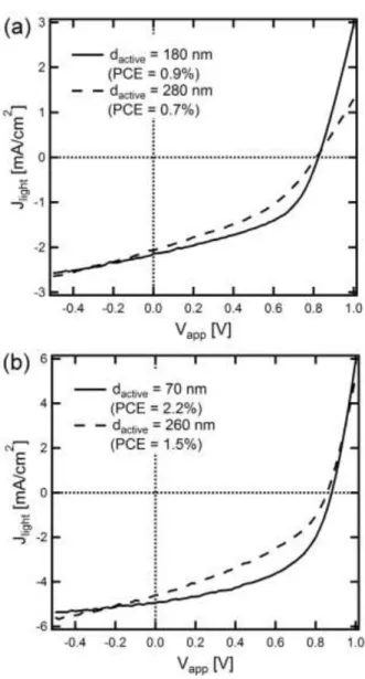
Figure 2.7) when using thick active layers. Since the primary reductions in performance for semi-transparent devices originate from reductions in Jsc (due to partial transmission
28
device configuration in spite of the drop in PCE. Furthermore, PCEs of 3.4%, 1.2%, and 4.5% were demonstrated for P3HT:PC60BM, MDMO-PPV:PC60BM, and
PCDTBT:PC60BM, respectively, when thin active layers were used and calcium
interlayers were added between the active layer a standard, thick aluminum cathode.
Figure 2.7 Current-voltage characteristics under 1 Sun illumination from glass side for semi-transparent devices with thin (< 10 nm) Al cathodes and (a) MDMO-PPV:PC60BM
and (b) PCDTBT:PC60BM active materials with varying active layer thickness, dactive. For
both device types (including P3HT:PC60BM from Figure 2.6), an increase in dactive causes
Figure 2.8 Local absorption or exciton generation rate (G) profiles in the active layer for devices with P3HT:PC60BM (top), MDMO-PPV:PC60BM (middle) and
PCDTBT:PC60BM (bottom). For λ = 473 nm illumination, the profile is weighted more
heavily close to or far from the PEDOT:PSS/BHJ interface for glass side and Al side illumination, respectively. All curves correspond to an incident intensity of 25 mW/cm2, typical of subsequent photocurrent measurements. Reprinted with permission from Ref. 56. Copy Right 2012, WILEY-VCH Verlag GmbH & Co. KGaA, Weinheim.
2.3.3 Local Absorption Profiles and Transport Distances
As mentioned above, local absorption profiles are determined using an auxiliary optics simulation that takes into account optical interference due to subsequent reflection and transmission of light at each internal device interface. Fig. 2.8 shows G of the three active materials under normal incidence of λ = 473 nm excitation wavelength when illuminating from the glass or semitransparent Al side of devices. G drops by around an order of magnitude across the active layer when illuminating from either side in P3HT:PC60BM device, because of its high absorption coefficient of at this wavelength,
30
in devices with MDMO-PPV:PC60BM and PCDTBT:PC60BM, due to the lower
absorption coefficients of these two blends. The significant difference between absorption profiles depending on illumination side can be characterized in terms of the carrier transport distance, De,h, i.e. average distance from electrons and holes are created
to their respective electrode to exit. For glass side illumination, De,htakes the form,
0 0 active active d h d
x G dx
D
G dx
(2.9)0 0
(
)
active active d activee d active h
d
x G dx
D
d
D
G dx
(2.10)Where x is the distance from the PEDOT:PSS/active layer interface. Similar expressions are used for Al side illumination.
We demonstrate the effect of both excitation wavelength and illumination side on De,h
in Fig. 2.9 In general, there is a larger difference in Dh when comparing glass and Al side
illumination at wavelengths where the polymer blend has the largest intrinsic absorption. In particular, for λ > 600 nm where intrinsic material absorption is weakest, Dhs for both
illumination sides tend toward dactive/2. In the case of P3HT:PC60BM devices with dactive =
310 nm, for λ = 473 nm glass side illumination, De = 237 nm and Dh = 73 nm, which
results in a transport distance for electrons as more than three times as for holes. Simply by illuminating from the Al side, the values of De and Dh are flipped thereby forcing
causes the transport to become insensitive to the illumination side. While this technique is similar to one previously reported,16 it does not require the use of both standard and inverted devices to achieve long De and Dh, respectively, which could cause changes in