Design and Implementation of an Efficient
Instruction Set for Ternary Processor
Satish Narkhede
Pune Institute of ComputerTechnology, Pune, India
Gajanan Kharate
Matoshri College of Engineering and Research Centre, Eklahare, Nasik, IndiaBharat Chaudhari
International Institute of Information Technology,Pune, India
ABSTRACT
Multi Valued Logic [MVL] is emerging as a promising choice for future computing technology. MVL has seen major advancement in the recent past due to several advantages offered by them over the binary logic, thus making it a thrust area for further research. The instruction set of the processor is its inherent entity. This paper presents design and implementation of an efficient instruction set for a ternary processor using Very-High-Speed Integrated Circuits, VHSIC Hardware Description Language [VHDL]. Twenty one instructions including various addressing modes such as register, direct and immediate mode are designed and implemented for 4-trit ternary processor. The required control signals are appropriately identified in the proposed design and enable the smooth operation of instructions. The designed 4 – trit instruction set signifies encouraging results that will pave the path for further developments in ternary processors.
General Terms
Digital Systems
Keywords
Multi Valued Logic, Ternary logic, VHDL.
1.
INTRODUCTION
Multi Valued Logic [MVL] has revolutionized the future of digital systems. The switching algebra in digital systems has expanded from binary to penta level, progressing through ternary and quaternary levels. Elena et al. describes MVL as painting a picture having all possible colors available, as against binary logic which includes just black and white. MVL displays a phenomenon that is never seen in binary, where the only two possible values are null and unity elements of Boolean algebra, possessing very specific properties [1]. An excellent review of the first developments of MVL and its applications to electronics, including a few circuit implementations, was presented by Epstein et al. [2] In a VLSI circuit approximately 70 % of the area is devoted to interconnection, 20 % to insulation and 10 % to devices. The binary logic is limited due to interconnect which occupies large area on VLSI chip [3]. Ternary Logic offered a potential solution to one of these major problems in VLSI System [4]. Advantages of ternary system over binary system are:
Reduced number of interconnections.
For example, (72)10 => (1100)3 =>(1001000)2 .
Reduced chip area.
Reduction in chip area in turn reduces chip delay. More information can be transmitted.
For example,
Using 4 bits, only 0 to 15 numbers can be represented in binary system while 0 to 80 in ternary system.
It also offers better utilization of transmission channels because of the higher information content carried by each line.
It gives more efficient error detection and correction codes.
Serial and serial parallel arithmetic operations can be carried out faster by using the ternary logic.
One of the main advantages of ternary logic is that it reduces the number of required computation steps. The number of address lines required to access the
address content can be reduced, i.e. hardware cost can be reduced.
Less memory requirement.
As the value of radix increases, the information carrying capacity of each connection also increases. Hence, MVL logical systems, for instance, a three-valued (radix 3) digital realization would be more appropriate than binary. Ternary (or three-valued) means a switching element, which switches among 3 levels namely true, false and intermediate. As ternary is radix-3 system, three levels are considered as logic ‘0’ = 0V, logic ‘Z’ = 2.5V and logic ‘1’ = 5V. So, this ternary processor should be capable of generating control signals for the instructions to be executed for a 4-trit microprocessor. In short, using ternary logic or radix-3 system, the number of address lines required to access the address content can be reduced, i.e. hardware cost can be reduced and more data can be occupied within less memory space. An evident advantage of a ternary representation over binary is economy of digits. To represent a number in binary system, one needs 58% more digits than that of ternary. It is therefore that the ternary is casting its applications in the field of Fuzzy logic, Machine Learning, Artificial Intelligence, Data Mining, Robotics, Digital signal processing, Digital control systems and Image Processing.
using CMOS ternary logic gates. Ali et al. [13] exploited the usefulness of neural network for designing a ternary ALU. Furthermore Kotiyal et al. [14] extended the reversible logic for a ternary barrel shifter. Use of various EDA tools like VHDL [15] for the simulation of ternary circuits have been also been reported in the literature.
The literature thus reports extensive efforts to develop combinational and sequential circuits using ternary logic. These designed circuits are certainly the essential components of a ternary processor. However, additionally, an efficient instruction set also forms an imperative component and plays a vital role in ternary processor. This issue has received comparatively less attention by the researchers and meager work is reported in the literature addressing this concern, to the best of the knowledge.
This paper proposes a novel approach to design and implement an efficient instruction set for ternary processor using VHDL. Twenty one instructions including various addressing modes such as register, direct and immediate mode are considered during this research. Section 2 describes the design of the proposed instruction set and the next section details the simulation results. Paper concludes with a discussion of the results and further scope for enhancing the designed instruction set.
2.
DESIGN OF THE INSTRUCTION SET
The objective of the proposed research is to design a 4-trit instruction set for a ternary processor using VHDL as a simulation tool. VHDL supports a top down and a bottom up approach by allowing higher level system design. VHDL also supports nine states, defining various logic levels like U, X, 0, 1, Z, W, L, H and -, that represent logic levels namely: uninitialized, unknown, logic 0, logic 1, high impedance, weak unknown, weak zero, weak one and don’t care, respectively [16]. The user defined packages, libraries and the user defined data types are the significant features of VHDL that are exploited for the design and simulation of the ternary instruction set which involves consideration of multiple logic levels.
VHDL can be used to model, simulate and describe ternary system where signals in the circuit can take tristate logic i.e., the usual true and false states, with a third transparent high impedance state. The third (intermediate) state can be metaphorically thought of as either an unambiguously true or unambiguously false. To demonstrate the use of VHDL as a ternary logic simulator, logic-0 is used to represent 0 volt, high impendence Z to represent 1volt and logic-1 to represent 2 volts. VHDL provides an effective way to connect several logic outputs to a single input, where all but one is forced to the high impedance state, allowing the remaining outputs to operate in the normal binary sense. This concept is commonly used for memory bank connection in computers and in connecting other similar devices to a common data bus. A large number of devices can therefore communicate over the same channel, simply by ensuring that only one is enabled at a time. VHDL package which include functions for ternary logical operations such as T-NOT, T_AND, T_NAND, T_OR, T_NOR, T_XOR are build successfully. It also includes ternary clock with clock period of 40 ns. Logical and arithmetic functions are defined in VHDL package and named as ‘std_terlogic’. The designed instruction set includes the instructions of various addressing modes namely, Register, Direct and immediate, as indicated in Table 1.
[image:2.595.313.544.169.743.2]The assigned op-codes and an example of each instruction are also depicted for comprehensiveness. Ternary instruction decoder is also designed that will decode the three trit op code from IR register. Instruction decoder is 3:27 decoder, which will select the corresponding instruction amongst the set of twenty one instructions. The control signals that drive the instruction set are also considered for implementation.
Table 1: The proposed instruction set for ternary processor.
Sr.
No Mnemonic Opcode
Addressing
Mode Example
1. T_ANA 00Z Register T_ANA B
2. T_ORA 001 Register T_ORA B
3. T_XRA 0Z0 Register T_XORA B
4. T_ADD 0ZZ Register T_ADDA B
5. T_ADC 0Z1 Register T_ADC B
6. T_SUB 010 Register T_SUB B
7. T_SBB 01Z Register T_SBB B
8. T_ICR 011 Register T_ICR
9. T_DCR Z00 Register T_DCR
10. T_RAL Z0Z Register T_RAL
11. T_RAR Z01 Register T_RAR
12. T_CMA ZZ0 Register T_CMA
13. T_ADDI ZZZ Immediate T_ADDI, 35
14. T_SUI ZZ1 Immediate T_SUI, 45
15. T_MVI A Z10 Immediate T_MVI A,20
16. T_MVI B Z1Z Immediate T_MVI B, 20
17. T_LDA Z11 Direct T_LDA, 20
18. T_MOV
A, B 100 Register T_MOV A,B
19. T_MOV
B, A 10Z Register T_MOV B,A
20. T_MOV
A, C 101 Register T_MOV A,C
21. T_MOV
Figure 1: Data flow diagram of the ternary processor.
3.
DATA FLOW AND SIMULATION
RESULTS
Figure 1 depicts the dataflow diagram for the proposed instruction set. Ten different control signals are generated as explained below:
PC_sig : To control in and out operation of the PC register
Y_Z_sig : To control in operation of Y register and out operation of Z register
R_W_sig : To control read and write operation from/on memory
A_sig : To control in and out operation of the A register
B_sig : To control in and out operation of the B register
C_sig : To control in and out operation of the B register
MAR_sig : To control in and out operation of the MAR register
MDR_sig : To control in and out operation of the MDR register
IR_sig : To control in and out operation of the IR register
END : To specify the end of the instruction
execution
selmux : To select either ALU or a constant
sel(0) : First trit (LST) of ALU select
sel(1) : Second trit of ALU select
sel(2) : Third trit (MST) of ALU select
Few control signals will control the register dataflow i.e in and out. For such a trit control signal,
When signal is ‘1’ => register out operation When signal is ‘Z’ => register in operation When signal is ‘0’ => No operation
A control signal specifies the read and write operation for memory.
When signal is ‘1’ => memory read operation When signal is ‘Z’ => memory write operation When signal is ‘0’ => No operation
Three trit control signals are used to select ALU operation i.e. sel(0), sel(1), sel(3). Selmux is the control signal which will select the one of the input to the ternary ALU. Input can be either accumulator or a constant ‘Z’. END signal will specify the end of the instruction and it will reset the two trit step counter. Processor can execute up to twenty three instructions. These instructions are performed in basically three steps: Fetch: Fetch the ternary op-code from the memory and
send it to the instruction register for decoding.
Decode: Decode the op-code in the instruction register and decide which instruction is to be executed.
Execute: Execute the decoded instruction by activating the appropriate control signals’ sequence.
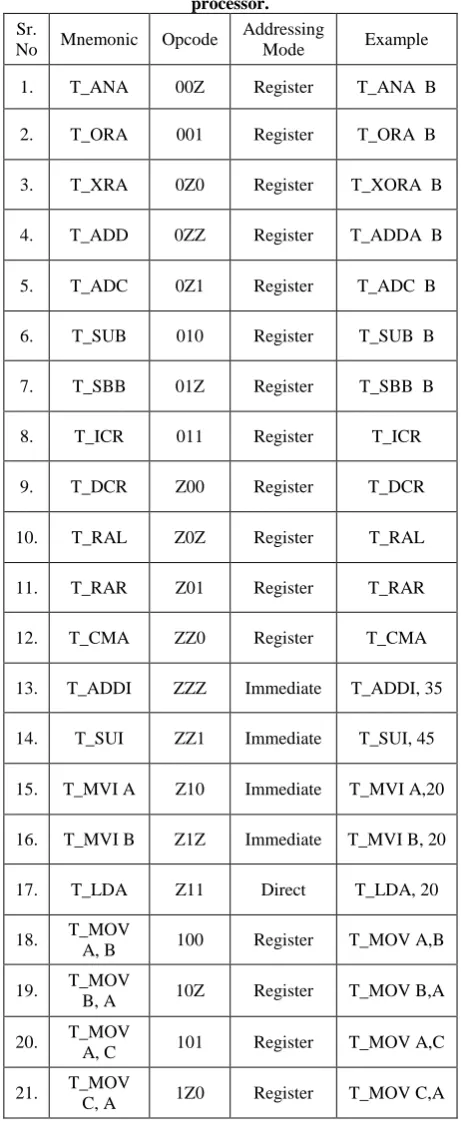
The dataflow diagram of the processor enables the working of the processor. Consider the instruction “T_MVI A, 00Z1” which is an instruction with immediate addressing mode. The opcode of the instruction “0Z10” is stored in the memory at one location and the immediate data “00Z1” is stored at the next location. In this instruction the immediate data “00Z1” is copied from the memory to the accumulator. The instruction is performed in a total of seven steps as shown below: Step 1:
Control signals: PC=>’1’, MAR=>’Z’, Y_Z=>’Z’, sel_mux=>’1’, sel_ALU=>”0Z1”, R_W=>’1’.
Operations performed:
First, the address of the opcode is transferred from the PC to MAR register and read signal is activated. The data then is read into the MDR register in the same cycle. At the same time, value in program counter is incremented in the ALU by “000Z”.
Step 2:
[image:3.595.53.282.422.672.2]The incremented value of program counter is updated. Step 3:
Control signals: MDR=>’1’, IR=>’Z’. Operations performed:
The opcode fetched into the memory data register is now copied into the instruction register.
Step 4:
Control signals: PC=>’1’, MAR=>’Z’, Y_Z=>’Z’, sel_mux=>’1’, sel_ALU=>”0Z1”, R_W=>’1’.
Operations performed:
Similar to step 1, the data at the next location, that is, the immediate data is now fetched and the value in program counter is again incremented in the ALU.
Step 5:
Control signals: Y_Z=>’1’, PC=>’Z’. Operations performed:
The incremented value of program counter is again updated.
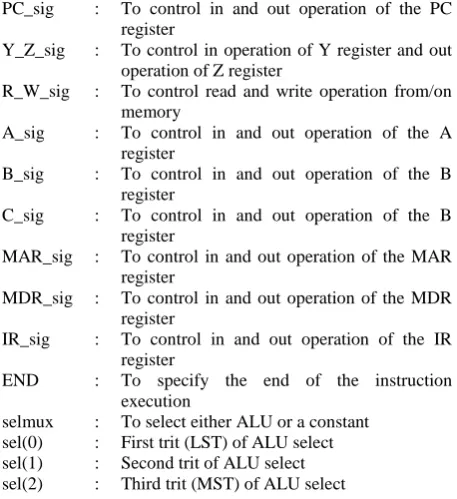
Step 6:
Control signals: MDR=>’1’, A=>’Z’. Operations performed:
The fetched immediate data is copied from the memory data register into the accumulator.
Step 7:
Control signals: End=>’1’. Operations performed:
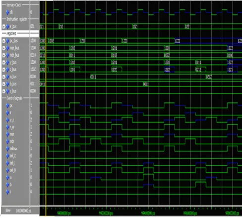
This indicates that the instruction has completed execution. Figure 2 (a)-(f) illustartes the step wise results indicating the described dataflow. Figure 3 depicts the simulation results of this instruction.
Internal Processor Bus
Y Z A T-MUX “000Z” Selmux = 1 ADD
Y_Z = ‘Z’
T-ALU Ternary Control Unit Registers Ternary Step Counter Ternary Instruction Decoder A B C
PC = 0000
MAR = 0000
MDR = 0Z10
IR
Memory
00 0Z10 Address Data
0Z 0011
01 010Z
Z0 00ZZ
ZZ 0100
Z1 0101
10 0Z0Z
1Z 001Z 11 00Z1 TALU
T1 R_W_Sig = ‘1’
PC= ‘1’
MAR= ‘Z’
DATA = 0000
Figure 2(a): Step 1, T1 cycle
Internal Processor Bus
Y
Z = 000Z A
T-MUX “000Z”
Y_Z = ‘1’ T-ALU Ternary Control Unit Registers Ternary Step Counter Ternary Instruction Decoder A B C
PC = 000Z
MAR
MDR = 0Z10
IR
Memory
00 0Z10 Address Data
0Z 0011
01 010Z
Z0 00ZZ
ZZ 0100
Z1 0101
10 0Z0Z
1Z 001Z 11 00Z1 TALU
T2
PC= ‘Z’
DATA = 000Z
Figure 2(b): Step 2, T2 cycle
Internal Processor Bus
Y Z A T-MUX “000Z” T-ALU Ternary Control Unit Registers Ternary Step Counter Ternary Instruction Decoder A B C
PC = 000Z
MAR
MDR = 0Z10
IR = 0Z10
Memory
00 0Z10 Address Data
0Z 0011
01 010Z
Z0 00ZZ
ZZ 0100
Z1 0101
10 0Z0Z
1Z 001Z 11 00Z1 TALU
T3
I(15) = ‘1’ MDR = ‘1’
IR= ‘Z’
MVI A, #04
DATA = 0Z10
[image:4.595.158.523.58.729.2] [image:4.595.322.534.72.366.2] [image:4.595.321.534.398.696.2] [image:4.595.63.272.452.752.2]Internal Processor Bus Y Z A T-MUX “000Z” Selmux = 1 ADD
Y_Z = ‘Z’
T-ALU Ternary Control Unit Registers Ternary Step Counter Ternary Instruction Decoder A B C
PC = 000Z
MAR = 000Z
MDR = 0011
IR
Memory
00 0Z10 Address Data
0Z 0011
01 010Z
Z0 00ZZ
ZZ 0100
Z1 0101
10 0Z0Z
1Z 001Z 11 00Z1 TALU
T4
R_W_Sig = ‘1’ PC= ‘1’
MAR= ‘Z’
DATA = 000Z
Figure 2(d): Step 4, T4 cycle
Internal Processor Bus
Y
Z = 0001 A
T-MUX “000Z”
Y_Z = ‘1’ T-ALU Ternary Control Unit Registers Ternary Step Counter Ternary Instruction Decoder A B C
PC = 0001
MAR
MDR = 0011
IR
Memory
00 0Z10 Address Data
0Z 0011
01 010Z
Z0 00ZZ
ZZ 0100
Z1 0101
10 0Z0Z
1Z 001Z 11 00Z1 TALU
T5
PC= ‘Z’
DATA = 0001
Figure 2(e): Step 5, T5 cycle
Internal Processor Bus
Y Z A T-MUX “000Z” T-ALU Ternary Control Unit Registers Ternary Step Counter Ternary Instruction Decoder
A = 0011
B
C
PC = 0001
MAR
MDR = 0011
IR
Memory
00 0Z10 Address Data
0Z 0011
01 010Z
Z0 00ZZ
ZZ 0100
Z1 0101
10 0Z0Z
1Z 001Z 11 00Z1 TALU
T6
A = ‘1’
MDR= ‘1’
DATA = 0011
Figure 2(f): Step 6, Cycle T6
4.
CONCLUSION
This paper proposes an efficient design of 4 trit instruction set for twenty one instructions with various addressing modes such as register, direct and immediate mode. The required control signals are appropriately identified in the proposed design and enable the smooth operation of instructions. The designed 4 – trit instruction set signifies encouraging results that will pave the path for further developments in ternary processors.
The issue of effectively designing the instruction set for a ternary processor has received comparatively less attention by the researchers and meager work is reported in the literature addressing this concern. It must therefore be emphasized that the performance of the proposed ternary instruction set though is extremely encouraging; it cannot be directly compared with the state of art methods. The depicted simulation results provide a strong foundation about the behavior of the ternary processor from the instruction – execution prospective; which is governed by the identified control signals.
[image:5.595.62.273.67.362.2] [image:5.595.324.534.71.387.2] [image:5.595.65.270.398.709.2]Figure 3: Simulation results of the instruction execution
5.
REFERENCES
[1] Elena Dubrova, ‘Multi-Valued Logic in VLSI:
Challenges and Opportunities’ Proceedings of
NORCHIP, vol. 99, pp. 340-350. 1999.
[2] Serran N, Martins J, Dias J, ‘A proposal for the
implementation of ternary digital circuits’,
microelectronics Journal 28, 1997, pp. 533-541.
[3] Gorde, K., Deshmukh. P.: ‘Design and Simulation of Ternary Logic Based Arithmetic Circuits’, Proceedings of the 2009 International Conference on Signals, Systems and Automation (ICSSA 2009). Universal-Publishers. com, 2010
[4] Rizwan, B.: ‘Current mode signaling in deep sub-micrometer global interconnects’, IEEE transactions on very large scale integration (VLSI) systems, 11(3), 2003, pp. 406-417.
[5] Stephen, H.: ‘High speed digital system design’, John Wiley and Sons, Inc. 2000, pp. 74-90.
[6] Sheng, L., Yong-Bin, K., Fabrizio, L.: ‘CNTFET- based design of ternary logic gates and arithmetic circuits’, IEEE transactions on nanotechnology, 10(2), March 2011.
[7] Satish Kumar, A., Sweta Priya, A., ‘Modeling of combinational circuits based on ternary multiplexers using VHDL’, International journal of computer science and engineering, 2(5), 2010, 1777-1791.
[9] Raychowdhury, A., Kaushik, R.: ‘A novel multiple valued logic design using ballistic carbon nanotube FETs’ , Proceedings of the 34th
IEEE international symposium on multiple valued logic (ISMVL ‘04), pp 14-19.
[10]Mozammel, K.: ‘Quantum ternary parallel adder / subtractor with partially –look-ahead carry’ Journal of system architecture, 2007, 53, pp 453-464.
[11]Mozammel, K.: ‘A recursive method for synthesis quantum / reversible quaternary parallel adder/ subtractor with look-ahead carry’ Journal of system architecture, 54 (2008) pp. 1113-1121.
[12]Dhande, A., Ingole, T.: ‘Design and implementation of 2 bit ternary ALU slice’ 3rd
International conferences sciences of electronics, technologies of information and telecommunication, march 2005, Tunsia pp. 1- 11.
[13] Ali, H., Hamdam, M., Rashid, M., Hamied, H., Issa, A., Kassem, A.: ‘A novel neural network ternary arithmetic logic unit’, The 23rd
international technical conference on circuits / systems, computers and communications (ITC-CSCC 2008), pp. 593-596.
[14] Kotiyal, S., Himanshu, T., Nagarajan, R.: ‘Design of A ternary barrel shifter using multiple valued reversible logic’, Proceeding of 10th
IEEE international conference on nanotechnology joint symposium with nano korea 2010, pp. 1104-1108.
[15] Rozon, C.: ‘On the use of VHDL as a multi-valued logic simulator’. Multiple-Valued Logic, 1996. Proceedings of 26th International Symposium on. IEEE, 1996, pp 110-115.