A Low Power 4 Bit Successive Approximation
Analog-To-Digital Converter Using 180nm
Technology
Jasbir Kaur1, Praveen Kumar2
1Assistant Professor, ECE Department, PEC University of Technology, Chandigarh, India 2PG Scholar, Electronics (VLSI Design), PEC University of Technology, Chandigarh, India
Abstract: In this paper, 4 bit successive approximation analog-to- digital converter (SAR ADC) has been designed. The design is using Cadence tool with 180nm CMOS technology in which supply voltage is 3.3V. The successive approximation has three components which are comparator, control logic and digital- to- analog converter.The SAR ADC is used widely in data acquisition techniques at the sampling rates higher than 10KHz like computer, microcontroller, microprocessor, TV etc.
Simulation result shows that proposed successive approximation analog-to-digital converter have a power efficiency or consumption of 3.323mwatt.
Keywords-- Comparator, Control logic, Digital-to-analog converter.
I. INTRODUCTION
ADC is an integral part of many electronic devices. It is used to convert the analog signal to digital signal. There are various type of ADC like counter type ADC, SAR ADC, pipeline ADC, sigma-delta ADC and flash type ADC. Pipeline ADC are used when higher resolution is required then that of flash ADC is required at the cost of lower sampling rate. Sigma-Delta ADC and counter type are slower in speed. Flash ADC also required larger area. SAR ADC provide good accuracy, good resolution, low cost and good speed. So the best ADC is SAR ADC. This paper is organized as follows. A brief introduction about SAR ADC is given in Section I. In section II, the conventional ADC architecture has been discussed. In section III, the proposed SCR ADC is explained. In Section IV, simulation and experiment result of conventional SAR ADC and proposed SAR ADC is shown. In section IV, conclusion and comparison of conventional SCR ADC and proposed SCR ADC is done.
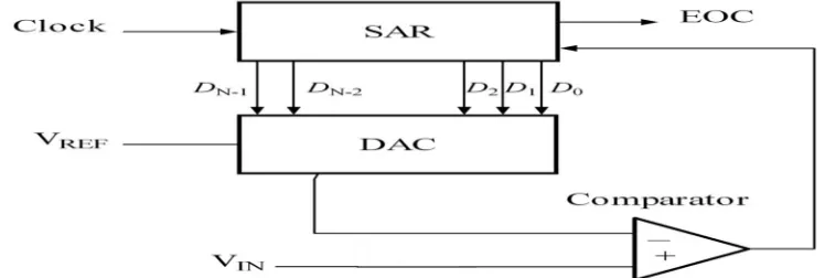
II. CONVENTIONAL ADC
[image:2.612.116.490.581.707.2]III. PROPOSED ADC
As discussed in section II the block diagram of conventional ADC is shown in figure1. The design procedure in the proposed ADC has been done by designing each block independently and the output waveform has been verified for each block. The blocks are control logic, Digital-to-Analog converter, comparator. Further in this section the each block is explained in detail its working and interfacing.
[image:3.612.96.518.233.413.2]A. control logic
Figure 2 show the control logic circuit by using sequencer and code register. The sequencer is a shift register which is initially reset and for every clock pulse it shift ‘1’ through the register. The output of a sequencer set a flip-flop in the coded register and the output of comparator is given as input to each coded register flip-flop. First of all it will set the MSB bit to ‘1’ and remaining bit to ‘0’ if the output of comparator is ‘1’ MSB bit remain at ‘1’ and the next bit is set to ‘1’. If the output of comparator is ‘0’ then MSB bit is set to ‘0’ and the next bit is set to ‘1’. This process continues until all bit are done.
Figure 2: Circuit Diagram of control logic
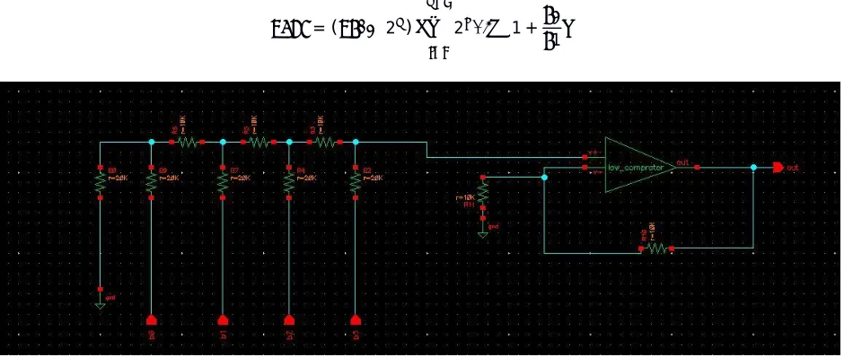
[image:3.612.72.542.505.704.2]B. Digital-to-Analog converter
Figure 3 shows the Digital-to-Analog converter circuit it consist of R-2R ladder and a comparator. It is used to convert the digital signal to analog singnal. The bit which near to comparator is the MSB bit and the bit which is far away from comparator is the LSB bit. The expression used to convert the digital signal to analog signal is
= ( ⁄2 ) 2 1 +
1
C. Comparator
Comparator used in ADCs plays very critical role. The parameters such as input offset voltage, propagation delay, power consumption and input range of comparator decides the parameters of Successive approximation ADC.
Comparator consumes considerable power in ADC circuits. As the resolution increases, the number of comparator increases and consequently, the power consumed and area also increases exponentially. At
[image:4.612.205.399.173.299.2]high frequencies, the noise generated in the comparator is considerable. Block diagram of comparator used in designed ADC is shown in Figure 4.
Figure 4. Block diagram of Comparator
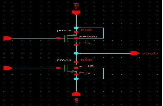
Comparator used in flash ADC is designed using CMOS technology so that it consumes minimum power. It consists of two stages 1) Differential amplifier
2) Common source amplifie 3) Differential Amplifier
The active loaded MOS differential amplifier schematic is shown in Figure 5. It consists of two matched transistors, NM0 and NM1, whose sources are joined together and biased by a constant-current source I. The constant current source is usually implemented by a MOSFET circuit of current mirror. Generally, each drain of differential amplifier is connected to the positive supply through a drain resistance, but active (current-source) loads are employed here. Whatever type of load is used, it is essential that the MOSFETs not enter the triode region of operation.
Transistor NM0 and NM1 are biased using constant current source which has been implemented using a current mirror circuit i.e. source of NM0 and NM1 are connected to each other and current source is applied to them. Current mirror has been implemented using NM2 and NM3. PM0 and PM1 are used as an active load in differential amp.
= and Ad = gm r0
Where Ad represents the differential gain of the differential amplifier, gm denotes the transcendence of MOS transistor and r0
denotes the output resistance of MOS transistor.
[image:4.612.202.416.530.707.2]D. Current Mirror
[image:5.612.193.420.106.241.2]The circuit of a simple MOS constant-current source is given by Figure 6.
Figure 6: Current mirror circuit
The heart of the circuit is transistor Q1, the drain of which is shorted to its gate, thereby forcing it to operate in the saturation mode with
ID1= k 'n
( )
( ) (VGS-Vtn)
2
The drain current of Q1 is supplied by current source, which in most cases would be outside the IC chip. Since the gate currents are zero where the current of current source is considered to be the reference current of the current source and is denoted IREF.
ID1 = IREF =
Now consider transistor Q2: It has the same as Q1; thus, if we assume that it is operating in saturation, its drain current which is the output current of the current source IO, will be
I0=ID2= k 'n
( )
( ) (VGS-Vtn)
2
The special connection of Q1 and Q2 provides an output current Io that is related to the reference current IREF by the aspect ratios of
the transistors. In other words, the relationship between Io and IREF is solely determined by the geometries of the transistors.
=( / )2
( / )1
1) Common Source Amplifier: The Schematic of the Common Source Amplifier is shown in the Figure 7.
[image:5.612.161.472.501.704.2]As shown in the schematic, the input to CS amplifier is given between source and gate terminal of NMOS and output is taken between source and drain of NMOS. PMOS acts as active load and input given to it keeps the amplifier in saturation region. The input of CS amplifier is the output of differential amplifier and gain of the CS amplifier is such that if the difference between V1 and V2 applied to the differential amplifier is positive then output saturates to the +VDD otherwise -VDD
Figure 8 illustrate the complete module of the successive approximation ADC. Each unit has been designed separately and verified by obtaining the output waveforms individually before interfacing and to be used in SAR ADC as a whole unit.
Figure 8: Block diagram of proposed ADC
IV. SIMULATION AND EXPERIMENTAL RESULTS
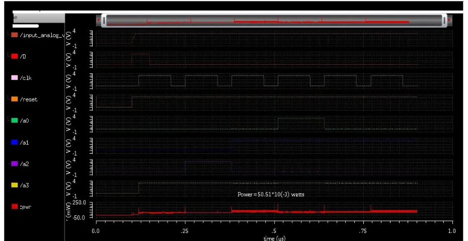
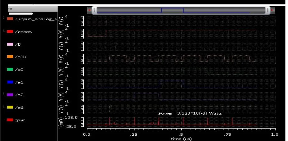
[image:6.612.93.558.466.706.2]Simulation of the conventional 4 bit SAR ADC and proposed SAR ADC comparator has been done with Cadence Analog tool using 180 nm technology. For simulation the input voltage is 3.3 V and VDD is also at 3.3V and the output are a3, a2, a1, a0 where a3 is the MSB bit and a0 is the LSB bit the output waveform obtained by tool is shown in Figure 9 and Figure 10 for conventional and proposed SAR ADC respectively. The power consumed is labeled on the output waveform for both ADC.
Figure 10: Simulation result of proposed SAR ADC
V. CONCLUSION
The proposed SAR ADC consumes less power. The comparison of power consumed between conventional SAR ADC and proposed SAR ADC is shown in table I. The conventional ADC consume 50.51mW power while the proposed ADC consume 3.323mW. Thus, this proposed SAR ADC ispower efficient and can be used in low power application.
Table I
Comparison of power consumed between conventional SAR ADC and proposed SAR ADC Arch.
Spec.
Conventional SAR ADC Proposed SAR ADC SAR ADC [9]
Technology GPDK 180nm GPDK 180nm 45nm
Power Supply 3.3V 3.3V 1 V
Resolution 4 bit 4 bit 4 bit
Input Analog Range 0~6V 0~6V 0~1V
Power Consumed 50.51mW 3.323mW 4mW
REFERENCES
[1] ALGN Aditya, G.RakeshChowdary , J. Meenakshi, M.S.Vamsi Krishna “Implementation of Low power Successive Approximation ADC for MAV’S”, IEEE International Conference on Signal Processing, Image Processing and Pattern Recognition 2013.
[3] SiamakMortezapour, Edward K. F. Lee “A 1V 8-Bit Successive Approximation Register in standard CMOS process”, IEEE Journal of SolidState Circuits, Vol.35, No.4, April 2009.
[4] Young-Kyun Cho, Young-DeukJeon, Jae –won Nam,Jong-Kee Kwon “A 9-bit 80 MS/s Successive Approximation Register Analog to Digital converter with a capacitor reduction Technique” ,IEEE Transactions on Circuits and Systems—Ii: Express Briefs, Vol. 57, No. 7, July 2010.
[5] Pieter J. A. Harpe, Cui Zhou, Yu Bi, Nick P. van derMeijs, XiaoyanWang,Kathleen Philips, Guido Dolmans, and Harmke de Groot “A 26 uW 8 bit 10 MS/s Asynchronous SAR ADC for Low Energy Radios”, IEEE Journal of Solid-State Circuits, Vol. 46, No. 7, July 2011.
[6] Guan-Ying Huang, Soon-Jyh Chang, Chun-Cheng Liu, Ying-Zu Lin “A 1-μW 10-bit 200-kS/s SAR ADC With a Bypass Window for Biomedical Applications” ,IEEE Journal of Solid-State Circuits, Vol. 47, No. 11, November 2012.
[7] Weibo Hu, Yen-Ting Liu, Tam Nguyen, DonaldY. C. Lie, Brian P. Ginsburg “An 8-Bit Single-Ended UltraLow-Power SAR ADC With a Novel DAC Switching Method and a Counter-Based Digital Control Circuitry” ,IEEE Transactions on Circuits And Systems—I: Regular Papers, Vol. 60, No. 7, July 2013. [8] Hur A. Hassan, Izhal Abdul Halin, Ishak Bin Aris , MohdKhair Bin Hassan “Design of 8-bit SAR-ADC CMOS” ,IEEE 2009.