Technology (IJRASET)
FPGA Implementation of Scalable Micro
Programmed FIR Filter using
Wallace Tree Multiplier
K.Karthikeyan1, K.Manivel2
1
PG Scholar, ME (Vlsi Design), Mahendra Engineering College, Namakkal, Tamilnadu, India.
2
Assistant Professor, Department ECE, Mahendra Engineering College, Namakkal, Tamilnadu, India.
Abstract— Finite Impulse Response filters are the most important element in signal processing and communication. FIR filter architecture contain multiplier, adder and delay unit. So, performance of FIR filter is mainly based on multiplier. In this paper we present FIR filter implementation of Wallace multiplier. This technique is used to improve the performance of delay, power and Area. The code is written in VHDL and it is simulated in ModelSim 6.3c and synthesis is done in Xilinx ISE 9.2i. Finally the design is implemented in Spartan-3 FPGA
Index Terms—FIR filter, Wallace Multiplier, VHDL.
I. INTRODUCTION
Since the speculation of digital signal process (DSP) is developed and applied to the engineering science world, digital filtering continually plays a really vital role. Digital filtering techniques is employed to suppress noise, enhance signal in hand-picked frequency ranges, constrain information measure, take away or attenuate specific frequencies and different special operations. Digital filters square measure classified into finite impulse response (FIR) and infinite impulse response (IIR) filters. FIR digital filters will have specifically linear section response and a really regular design, and suffer less from the consequences of finite word length as compared with IIR digital filters. This thesis presents the planning an implementation of such a filter supported redundant binary variety systems. The most parts of FIR filter square measure adder, multiplier factor and delay. The carry propagation delay could be a limiting issue of the adder and multiplier factor. Supported redundant variety, adders and multipliers square measure designed in such some way that the propagation delay is reduced of the FIR filter.
The advantages of full custom square measure most circuit performance, minimum style size, and minimum high-volume cost. Finally, planning box-car FIR filter and 3-tap FIR (multiplier constant 4-bit) filter will function a basic of IC style students to figure with as a tool in their understanding of digital style. It's additionally a stepping-stone for college kids in planning different CMOS chips victimization the 90nm CMOS technology and to encourage them to form enhancements within the style. The basic operation in digital signal process is filtering. This operation is wide utilized in several electronic devices to cancel a part of signal that's redundant or damages the signal. The digital filter is delineate by distinction equation in time domain and by transfer operate in frequency domain. There square measure 2 basic sorts of digital filters: Finite impulse response (FIR) filters and infinite impulse response (IIR) filters. The each sorts of filters have some blessings and drawbacks that square measure summarized in Table one. The main disadvantage of a FIR filter is high order of the filter as compared with IIR filter with just about an equivalent frequency response. that the size, consumption of power and computing time of a FIR filter square measure on top of IIR filter. The one in all the solutions of this drawback is use interpolated FIR (IFIR) filter that considerably reduces order of the filter. Structure of IFIR filter is delineate below. Additional details
regarding options of FIR and IIR filters is found in [3].
II. MOTIVATION AND GOALS
Technology (IJRASET)
transportable, battery operated systems because it extends battery life. Low power dissipation additionally helps cut back the packaging value (plastic rather than ceramic), eliminate / cut back cooling (heat sinks) overhead and increase the responsibleness of the device. For the need of high-speed and low-power applications, the event and implementation of high-speed FIR digital filters want each augmented similarity and reduced complexness so as to fulfill each rate and power dissipation goals. During this thesis, FIR filter is meant supported RNS to realize high speed operation. Bottom-up style flow is employed for optimum circuit performance, minimum style size, and minimum high-volume cost.
III. VLSI DESIGN FLOW
A. Introduction on Bottom-up and Top-down Design Flow
The styleer sometimes follows some design phases to form his project. At the start the designer needs to specify the practicality of the system. Basic blocks of the hardware square measure known and their interfaces, composed of information and management signals, are fixed. Today, there square measure 2 principal ways that to style a VLSI circuit with ancient tools that are developed in these last years. The styleer will opt for at discretion AN approach bottom-up or a top-down flow however generally the selection is forced in consequence of explicit design needs logic gate structure. Top-down could be a method of unvarying refinements. The designer starts with a prime read of the system and decomposes single blocks into smaller ones. Bottom-up flow starts with low-level building blocks and interconnects them to larger ones. In reality, these 2 techniques don't seem to be terribly incompatible and, for example, the designer can even prefer to use explicit successful cells and to try to not bit their structure at intervals a top-down approach [10]. The approach bottom-up is desirable in digital style if the designer wishes to plain a specific cell achieving carrying out with transistors full-custom designed so he needs to duplicate this structure in his project.
B. Bottom-Up Design Flow
The bottom-up style flow is given in Fig one.3.1. The bottom-up style flow starts with a collection of style specifications. The “specs” usually describe the expected practicality of the designed circuit additionally as different properties like delay times, area, etc. To fulfill the assorted style specifications sure style trade offs (area verses delay) square measure needed [10].
C. Schematic Capture
A Schematic Editor is employed for capturing (i.e. describing) the transistor-level style. The Schematic Editors give straightforward, intuitive means that to draw, to position and to attach individual parts that form up the planning. The ensuing diagram should accurately describe the most electrical properties of all parts and their interconnections. Additionally enclosed within the schematic square measure the provision connections (VDD and gnd), additionally as all pins for the input and output signals of the circuit. From the schematic, a netlist is generated, that is employed in later stages of the planning. The generation of an entire circuit schematic is thus the primary vital step of the transistor-level style.
D. Symbol Creation
A symbol read of the circuit is additionally needed for a few of the next simulation steps or for documentation functions. Thus, the schematic capture of the circuit topology is sometimes followed by the creation of an emblem to represent the whole circuit. The form of the icon to be used for the image might recommend the operate of the module (logic gates – AND, OR, etc.), however the default image icon could be a straightforward rectangular box with input and output pins. The image creation will facilitate the
circuit styleer to form a system level design consisting of multiple hierarchy level. VLSI Realization of Area efficient FIR Filters
IV. MULTIPLIERS
Technology (IJRASET)
together.
A. Wallace Tree Multiplier
A Wallace tree multiplier is an efficient implementation of a digital circuit that multiplies two integers. The Wallace tree has three steps:
1) Multiply (AND operation) each bit of one of the arguments, by each bit of the other, yielding n2 results. Depending on position
of the multiplied bits, the wires carry different weights, for example wire of bit carrying result of a2b3 is 32 .
2) Reduce the number of partial products to two by layers of full and half adders.
3) Group the wires in two numbers, and then add them with a conventional adder
B. Architecture of 4x4 Wallace Tree Multiplier
[image:4.612.124.481.269.394.2]Wallace‟s strategy is to combine the partial product bits at the earliest opportunity, which leads to the fastest possible design. The
Figure 2 shows the architecture of 4x4 Wallace Tree Multiplier.
Figure 2: Architecture of 4X4 Wallace Tree multiplier
C. Hardware Architecture
Field Programmable Gate Arrays (FPGAs) can be reprogrammed as many times in order to achieve the desired result. The major design benefit in this lies in the ability to test designs that might work. Prior to the development of the FPGA, the fabrication process can be quite expensive and very time consuming. The use of FPGAs in the design process allows the more design flexibility, and reducing a cost and developing time. If the design fails after being tested on a FPGA, the designer can simply rework the design and download it again to the FPGA. Use of an FPGA would thus eliminate the loss in development time caused by a faulty initial design, as well as giving the designer knowledge of whether or not the design works.
D. Wallace Tree Multiplier
The Wallace tree multiplier is a high speed multiplier. The summing of the partial product bits in parallel using a tree of carry-save adders became generally known as the ”Wallace Tree (WT)”.
Technology (IJRASET)
1) Formation of bit products.
2) Reduction of the bit product matrix into a two row matrix by means of a carry save adder.
3) Summation of remaining two rows using a faster Carry Look Ahead Adder (CLA).
E. Complexity Wallace multiplier
It is the modified version of Wallace multiplier. It has less half adders than the normal Wallace multiplier. The partial products are formed by N^2 AND gates. The partial products are arranged in an “inverted triangle” order. The modified Wallace reduction method divides the matrix into three row groups [15].
1) Use full adders for each group of three bits in a column like the conventional Wallace reduction.
2) A group of two bits in a column is not processed, that is, it is passed on to the next stage (in contrast to conventionalMethod).
Single bits are passed on to the next stage as in the conventional Wallace reduction.
3) The only time half adders are used is to ensure that the number of stages does not exceed that of a conventional
F. Wallace Tree Multiplier Architecture
A Wallace tree multiplier is an efficient hardware implementation of a digital circuit that multiplies two integers. Wallace tree reduces the number of partial products and use carry select adder for the addition of partial products. Wallace tree is known for their favorable computation time, when adding multiple operands to two outputs using 3:2 or 4:2 compressors or both. Wallace tree guarantees the lowest whole delay [5].
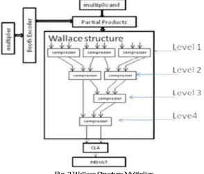
[image:5.612.157.451.337.589.2]Fig. 2 Wallace Structure Multiplier
Fig. 2 shows nine operands Wallace structure, where 3:2 compressors compress the data having three bit inputs and two multi-bit outputs. 4:2 compressors compress the data having four multi-multi-bit inputs and two multi-multi-bit outputs.
In fig. 3 blue circles represent full adder and red circle represent the half adder. Wallace tree has three steps [6]:-
1. Multiply each bit of multiplier with same bit position of multiplicand. Depending on the position of the multiplier bits generated partial products have different weights.
2. Reduce the number of partial products to two by using layers of full and half adders.
Technology (IJRASET)
[image:6.612.189.421.537.677.2]V. RESULTS
Fig. 3 Graphical Comparison of Power
The graph shows that the power of the previous FIR Filter design is more as compared to proposed design, hence we can say that the proposed FIR filter design using Wallace multiplier is less power consuming than the previous design which is our desired result and it will increase the efficiency.
Fig.4 Graphical Comparison of Delay
The graph shows that the delay of the previous FIR filter designs is more as compared to proposed design, hence we can say that the proposed FIR filter design using Wallace multiplier is faster than the previous designs which is our desired result and it will increase the efficiency by decreasing time complexity.
Fig.5 Graphical Comparison of Delay
Technology (IJRASET)
[image:7.612.148.467.117.229.2]which is our desired result and it will increase the efficiency by decreasing the complexity of circuit and also the cost of manufacturing of a chip.
Table 1 Comparison
The above table indicates the overall comparison of all parameters of the system i.e., it is clear from the table that proposed design is better in all the fields.
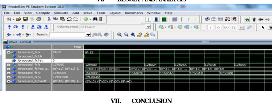
VI. RESULT AND ANALYSIS
VII. CONCLUSION
Table 1 shows the Comparison of Previous Designs and Proposed Wallace Multiplier Design. It was clear that there is a decrease in circuitry, power consumption, time consumption as compared to the previous designs. The code is written in VHDL. It is simulated by using ModelSim 6.3c. Synthesis is done in Xilinx ISE 9.2i. It is implemented in Spartan XC3s400. The proposed design is efficient to use in DSP applications.
REFERENCES
[1] International Standard : ISO/CD17361 “Intelligent Transport system-Lane Departure warning system Performance Requirements and Test Procedure, June 23, 2003.
[2] G. Oklobdzija, “High-Speed VLSI Arithmetic Units: Adders and Multipliers”, in “Design of High-Performance Microprocessor Circuits”, Book edited by A. Chandrakasan, IEEE Press, 2000
[3] Zhijun Huang, High level optimization techniques for low power multiplier design University of California, langels, 2003.
[4] L. Ciminiera, P. Montuschi, ”Carry-Save Multiplication Schemes Without Final Addition”, IEEE Transaction on Computer, vol. 45, no. 9, Sep. 1996. [5] M Bansal, "High performance pipelined signed 64*64-bit multiplier using radix-32 modified Booth algorithm and Wallace structure", International Conference
on Computational Intelligence and Communication Systems, 2011( 978-0-7695-4587-5/11)
[image:7.612.73.542.278.457.2]