Technology (IJRASET)
Implementation of Unsigned Multiplier Using
Area-Delay-Power Efficient Adder
Nalina R1, Ashwini S S2, Dr. M Z Kurian3
1
M.Tech, Student (VLSI & Embedded Systems) , 2Department of ECE
3
Professor and Head,Department of ECE SSIT, Tumkur, Karnataka, India
Abstract--Multiplication and addition are most widely and oftenly used arithmetic computations performed in all digital signal processing applications. Multiplication is the basic arithmetic operation which is present in many part of the digital computer especially in signal processing systems such as graphics and computation system. It requires substantially more hardware resources and processing time than addition and subtraction. In fact, 8.72% of all the instruction in typical processing units is multiplication. This paper deals with the basic multiplier that is shift and add multiplier. Accurate operation of the shift and add multiplier is mainly influenced by the performance of the adder. So performance of the adder enhances the performance of the multiplier. Hence, to design a better architecture the basic adder blocks must have reduced delay time consumption and area efficient architectures. This paper, involves the implementation of unsigned multiplier using area, delay and power efficient adder. This design will be developed using Verilog programming language and implementing using Field Programmable Gate Array (FPGA) platform.
Keywords – Modified Carry Select Adder (MCSLA), Half Sum Generation (HSG), Carry Generation (CG), Carry Selection (CS), Full Sum Generation (FSG).
I. INTRODUCTION
In arithmetic logic operation multiplication is an important fundamental function. Performance of a DSP system is limited by its multiplication performance and since, multiplication control the execution time of the DSP algorithms, therefore speed of the multiplier is much required. Multiplication time is the dominant factor in determining the instruction cycle time of a DSP chip. With an ever-increasing pursuit for greater computing power on battery-operated mobile devices, design has shifted from optimizing delay time area size to minimizing power dissipation while still maintaining the high performance. The low power and high speed VLSI can be implemented with different logic style. The three important factors for VLSI design are area, delay and power. There are many proposed methods and high speed and each logic design has its own advantages in terms of speed and power.
All complex and simple digital multiplication is based on addition. An area efficient, fast and accurate operation of a digital system is greatly depends on the performance of the basic adders. Adders are very important component in digital logic design because of their wide use in these systems. Hence, to design a better architecture the basic adder blocks must have reduced delay time consumption and area efficient architectures. In computers and other processors, adders are not only used in the arithmetic logic unit, but also in other parts of the processor. They are used to calculate addresses and other applications. Some other applications of adders are in Multiply – Accumulate (MAC) structures. Adders are also used in high speed integrated circuits and in digital signal processing to execute various algorithms like FIR and IIR. Design of low power, area efficient high speed data path logic systems are the most substantial areas in the research of VLSI design.
Technology (IJRASET)
Shift-and-add multiplication is similar to the multiplication performed by paper and pencil. This method adds the multiplicand B to itself Q times, where Q denotes the multiplier. To multiply two numbers, the algorithm is to take the digits of the multiplier one at a time from right to left, multiplying the multiplicand by a single digit of the multiplier and placing the intermediate product in the appropriate positions to the left of the earlier results. This multiplier uses the operation of additions in the operation of multiplication. The addition operations repeated and shifting results in the multiplication operation. For addition operation an efficient adder is used. The main logic of this adder is the carry select operation is scheduled before the calculation of final-sum.
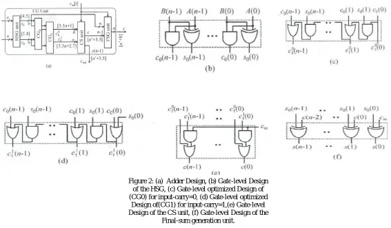
III. ADDER FOR SHIFT AND ADD MULTIPLIER
The block diagram of an adder is shown in figure 2a. It consists of one HSG unit, one FSG unit, one CG unit, and one CS unit which is given in figure (2b)-(2f). The CG unit is composed of two CGs (CG0 and CG1]) corresponding to input-carry '0' and' 1 '. The HSG receives two n-bit operands (A and B) and generate half-sum word S0 and half-carry wordC0 of width n bits each. Both CG0 and CG1 receive S0 and C0 from the HSG unit and generate two n-bit full-carry words c10and c11 corresponding to input-carry '0'
and' 1', respectively. The logic circuits of CG0 and CGI are optimized to take advantage of the fixed input-carry bits. The optimized designs of CG0 and CGI arc shown in Fig. (2c) and (2d), respectively. The CS unit selects one final carry word from the two carry words available at its input line using the control signal Cin. It selects c10 when Cin = 0; otherwise, it selects c11. The CS unit can be
implemented using an n-bit 2-to-1 MUX. However, we find from the truth table of the CS unit that carry words c10 and c11 follow a
specific bit pattern. If c10 (i) = '1', then c11 (i) = 1, irrespective of S0(i) and C0 (i) , for 0 < I < n-1.This feature is used for logic
optimization of the CS unit. The optimized design of the CS unit is shown in Fig, (2e), which is composed of n AND-OR gates. The final carry word C is obtained from the CS unit. The MSB of C is sent to output as Cout, and (n - 1) LSBs are XORed with (n - 1) MSBs of half-sum (S0) in the FSG [shown in Fig. (2f)] to obtain (n - 1) MSBs of final-sum (s). The LSB of S0 is XORed with Cin to obtain the LSB of S.
Figure 2: (a) Adder Design, (b) Gate-level Design of the HSG, (c) Gate-level optimized Design of (CG0) for input-carry=0, (d) Gate-level optimized
Design of(CG1) for input-carry=1,(e) Gate-level Design of the CS unit, (f) Gate-level Design of the
[image:3.612.30.597.191.522.2]Technology (IJRASET)
IV. RESULTSThis work has been developed using Xilinx tool. Figure3 shows theSimulation Result of an Adder. Figure4 shows theSimulation Result of the proposed multiplier. Table I shows the comparison between the multiplier using modified CSLA and the multiplier using efficient adder. The parameters on which they are compared are area, delay and power. The proposed multiplier has less number of gates and hence less area and power consumption of proposed multiplier is reduced. It is clear that power, area and delay of 16-bit proposed multiplier is reduced as compared to the multiplier using modified CSLA.
Figure3: Simulation Result of an Adder
Figure4: Simulation Result of the proposed multiplier
TABLE I
Comparison of area and delay complexities of proposed multiplier and multiplier using modified CSLA
Parameters Multiplier
Using Efficient
Adder
Multiplier Using MCSLA
Area 62 72
Delay 6.691ns 21.334ns
Technology (IJRASET)
V. CONCLUSIONPower, delay and area are the constituent factors in VLSI design that limits the performance of any circuit. An unsigned multiplier using area, delay and power efficient adder is successfully developed. This design is developed using Verilog programming language and simulated using Xilinx ISE 14.5 and implemented using Field Programmable Gate Array (FPGA) platform. The simulation of each system is done and then integrated to produce final output. The Proposed multiplier using efficient adder design involves significantly less area, delay and power than the recently proposed multiplier using Binary to Excess-1 based carry select adder.
REFERENCES
[1] Kuldeep Rawat, Tarek Darwish and Magdy Bayoumi, “A low power and reduced area Carry Select Adder”, 45th Midwest Symposium on Circuits and Systems, vol.1, pp. 467-470, March 2002.
[2] Y. Kim and L.-S. Kim, "64-bit carry-select adder with reduced area "Electron. Lett. vol. 37, no. 10, pp. 614- 615, May 2001. [3] J. M. Rabaey, Digtal Integrated Circuits-A Design Perspective.Upper Saddle River, NJ: Prentice-Hall,2001.
[4] Cadence, "Encounter user guide, " Version 6.2.4, March 2008.
[5] R. Priya and J. Senthil Kumar, “ Enhanced area efficient architecture for 128 bit Modified CSLA”, International Conference on Circuits, Power and Computing Technologies,2013.
[6] Shivani Parmar and Kirat pal Singh,”Design of high speed hybrid carry select adder”,IEEE ,2012.