N A N O E X P R E S S
Open Access
External quantum efficiency response of thin
silicon solar cell based on plasmonic scattering of
indium and silver nanoparticles
Wen-Jeng Ho
*, Yi-Yu Lee and Shih-Ya Su
Abstract
This study characterized the plasmonic scattering effects of indium nanoparticles (In NPs) on the front surface and silver nanoparticles (Ag NPs) on the rear surface of a thin silicon solar cell according to external quantum efficiency (EQE) and photovoltaic current–voltage. The EQE response indicates that, at wavelengths of 300 to 800 nm, the ratio of the number of photo-carriers collected to the number of incident photons shining on a thin Si solar cell was enhanced by the In NPs, and at wavelengths of 1,000 to 1,200 nm, by the Ag NPs. These results demonstrate the effectiveness of combining the broadband plasmonic scattering of two metals in enhancing the overall photovoltaic performance of a thin silicon solar cell. Short-circuit current was increased by 31.88% (from 2.98 to 3.93 mA) and conversion efficiency was increased by 32.72% (from 9.81% to 13.02%), compared to bare thin Si solar cells.
Keywords:Conversion efficiency; External quantum efficiency (EQE); Nanoparticle; Plasmonic scattering; Silicon solar cell
Background
Photovoltaic energy is a viable renewable source of energy for coming generations. Unfortunately, the cost per unit of electricity generated by a photovoltaic system is higher than the retail price of electricity generated using conventional methods. Making power from photovoltaic devices com-petitive with other technologies, such as fossil fuels, will re-quire considerable reductions in the cost of manufacturing. Current photovoltaic technology is based on bulk wafer-based crystalline silicon (C-Si) technology, which depends on the cost of Si materials and processing. Thus, the easiest way to reduce the costs of these devices is to reduce the amount of materials by producing thinner devices (thin Si solar cells; approximately 100 to 150μm-thick) rather than traditional silicon solar cells (approximately 300-μm-thick). Many light-trapping methods have been proposed to achieve high efficiency without incurring high costs. Metal-lic nanoparticle plasmonic appMetal-lications have been widely studied to enhance photovoltaic performance [1-4]. The resonance of most metallic nanoparticles is in the visible or infrared regions of the electromagnetic spectrum; however,
this also depends on size, shape, and spacing of the metallic particles as well as the dielectric properties of the surround-ing medium [5-7]. Most previous studies have shown that silver (Ag) and gold (Au) nanoparticles (NPs) can be used in bulk wafer-based C-Si solar cells or thin-film Si solar cells where the NPs are deposited on one surface of the solar cells [1,3,4,8-12]. However, few studies have examined the effects of metallic NPs deposited on the front and back surfaces of a thin Si solar cell [13].
This study fabricated solar cells with indium (In) NPs [14,15] on the front surface and Ag NPs on the rear sur-face. We then examined the degree to which photovoltaic performance was enhanced by the plasmonic scattering of In NPs and Ag according to external quantum efficiency (EQE) and measurements of photovoltaic current–voltage (I-V). EQE was enhanced at wavelengths of 300 to 800 nm thanks to In NPs and at 1,000 to 1,200 nm thanks to the Ag NPs. Short-circuit current was increased by 31.88% (from 2.98 to 3.93 mA), and conversion efficiency was in-creased by 32.72% (from 9.81% to 13.02%), compared to those of bare thin Si solar cells.
* Correspondence:[email protected]
Department of Electro-Optical Engineering, National Taipei University of Technology, No. 1, Sec. 3, Zhongxiao E. Rd, Taipei 10608, Taiwan
© 2014 Ho et al.; licensee Springer. This is an Open Access article distributed under the terms of the Creative Commons Attribution License (http://creativecommons.org/licenses/by/4.0), which permits unrestricted use, distribution, and reproduction in any medium, provided the original work is properly credited.
Methods
A 250-μm-thick p-type (boron doped) Si wafer with re-sistivity of 1 to 10 Ωcm and (100) orientation was cut into small samples (1 × 1 cm2) and polished on one side for the fabrication of solar cells. The back side of the Si samples was then ground down to obtain Si samples of 120-μm-thick. After standard RCA cleaning, the thin Si samples were coated with a phosphorus liquid source (Phosphorosilicafilm; Emulsitone Co., Washington, NJ, USA) on the front surface using a spin-on film (SOF) technique at a speed of 6,000 rpm for 20 s. This was followed by prebake processing on a hot plate at 200°C for 5 min for the removal of solvents and 400°C for 10 min to promote cross-linking. Both sides of the sam-ples were then capped with a 250-nm-thick SiO2 layer
using e-beam evaporation and heated in a rapid thermal annealing (RTA) chamber under an N2 atmosphere at
900°C for 2 min in order to diffuse the phosphorus
resulting in an n+-Si emitter approximately 0.4 μm in thickness. Following phosphorus diffusion, the samples were soaked in an HF solution to remove the SiO2caps
as well as the layer of phosphorus oxide. The diffusion profile was examined using secondary ion mass spectrometry (SIMS). We then deposited 20-nm-Ti/200-nm-Al films on the front surface using patterns of photo-resist. Finally, the samples were isolation etched in KOH solution using a photolithography process to obtain individual areas 4 × 4 mm2.
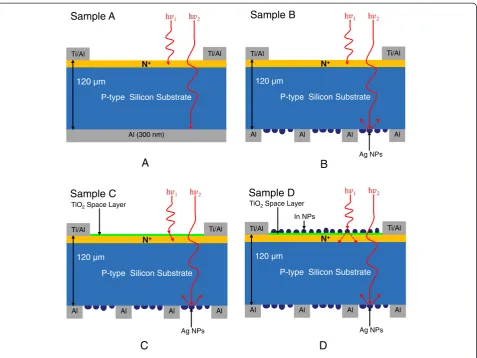
[image:2.595.307.540.89.256.2]To characterize the external quantum efficiency (EQE) response of thin silicon solar cells, the samples were la-beled A, B, C, and D. Sample A had a 300-nm-thick Al film deposited on the rear surface using e-beam evapor-ation, which was then annealed in an RTA chamber to produce a bare thin silicon solar cell. Sample B had a 300-nm-thick Al film deposited on the rear surface in grid-patterns with 60% coverage using photo-resist. This was
Figure 1SEM image showing the sizes and profiles of Ag NPs.
0 20 40 60 80 100 120 140 160 180 200 220 240 260 280 300 320 340 0
5 10 15 20 25 30 35 40
P
ar
ti
c
les
A
m
ount
[image:2.595.59.288.89.257.2]Particles Diameter (nm) Ag Particles Coverage: 48.23% Average Diameter: 100 nm
[image:2.595.57.292.534.704.2]Figure 2Ag NPs particle size distribution calculated by analyzing the SEM image using J-image software.
Figure 3SEM image showing the sizes and profiles of In NPs.
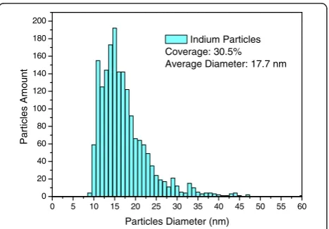
0 5 10 15 20 25 30 35 40 45 50 55 60 0
20 40 60 80 100 120 140 160 180 200
Indium Particles Coverage: 30.5% Average Diameter: 17.7 nm
Pa
rtic
le
s
A
mo
u
n
t
Particles Diameter (nm)
[image:2.595.306.540.543.706.2]followed by the deposition of a 30-nm-thick Ag film on the rear surface, which was annealed at 300°C under N2
for 3 min to form Ag NPs. The size and profile of the Ag NPs were examined using electron scanning microscopy (SEM; LEO 1530, Zeiss, Germany), the results of which are presented in Figure 1. Particle size distribution was calculated by analyzing the SEM image using J-image soft-ware, as shown in Figure 2. Sample C had a 30-nm-thick TiO2spacing layer deposited on the front surface of the
cell with Ag NPs and an Al electrode on the rear surface. Finally, sample D had a 3.8-nm-thick indium film depos-ited on the TiO2layer of the cell with Ag NPs and an Al
electrode on the rear surface, which was then annealed at 200°C under H2for 30 min to form In NPs. This resulted
in a plasmonic solar cell with In NPs on the front surface and Ag NPs on the rear surface. The size and profile of the In NPs were examined using SEM, the results of which are presented in Figure 3. Particle size distribution was calculated by analyzing the SEM image using J-image software, as shown in Figure 4. The schematic diagram of samples A, B, C, and D were given as shown in Figure 5A, B,C,D.
Ti/Al Ti/Al
Al (300 nm) P-type Silicon Substrate
N+
120
Sample A
Al Al Al
Ti/Al Ti/Al
Al
P-type Silicon Substrate
N+
Ag NPs 120
Sample B
Al Al Al
Ti/Al Ti/Al
Al
P-type Silicon Substrate
N+
Ag NPs TiO2Space Layer
In NPs
120
Sample D
Al Al Al
Ti/Al Ti/Al
Al
P-type Silicon Substrate
N+
Ag NPs TiO2Space Layer
120
Sample C
C
D
[image:3.595.61.539.87.445.2]A
B
Figure 5Schematic diagram of samples A (A), B (B), C (C), and D (D).
0.0 0.1 0.2 0.3 0.4 0.5 0.6
0.0 0.5 1.0 1.5 2.0 2.5 3.0 3.5 4.0 4.5
Cu
rre
n
t
(mA)
Voltage (V) B: Cell with Ag NPs A: Bare Cell
Figure 6Photovoltaic I-V of bare solar cell (sample A) and cell with Ag NPs (sample B).
Hoet al. Nanoscale Research Letters2014,9:483 Page 3 of 8
[image:3.595.304.540.529.702.2]To examine the electrical and optical properties of the proposed solar cell, we measured the photovoltaic current-voltage (I-V) and EQE in each stage of processing. The con-tribution of the plasmonic scatterings of In NPs and Ag NPs was characterized according to EQE response at wave-lengths between 300 and 1,000 nm (Enli Technology Co., Ltd., Kaohsiung City, Taiwan). The short-circuit current (Isc), open-circuit voltage (Voc), and conversion efficiency
(η) were obtained using photovoltaic I-V measurements under one-sun AM 1.5 G (1,000 mW/cm2at 25°C) solar simulation. The solar simulator (XES-151S, San-Ei Electric Co., Ltd., Osaka, Japan) was calibrated using a National Re-newable Energy Laboratory (NREL)-certified crystalline sili-con reference cell (PVM-236) prior to measurements.
Results and discussions
EQE is the ratio of the number of photo-carriers collected by the solar cell to the number of photons of a given energy (wavelength) that strike the surface of a solar cell from out-side. If all photons at a particular wavelength were absorbed and the resulting minority carriers were collected, then the quantum efficiency at that particular wavelength would be unity. The quantum efficiency of photons with energy below the band gap is zero. Generally, the quantum effi-ciency of a solar cell indicates the amount of current that the cell will produce when irradiated by photons of a par-ticular energy (wavelength). Integrating the quantum effi-ciency of a cell over the entire solar energy spectrum would make it possible to evaluate the amount of current that the cell could produce when exposed to sunlight. Therefore, the short-circuit current density (Jsc) of a photovoltaic
de-vice is found by convolving the EQE with AM 1.5 G solar energy spectrum
Jsc¼ Zλn
λ1
EQEð Þλ ⋅λ⋅q
hc⋅EAM1:5Gð Þλ dλ
where q is the elementary charge, h is Planck's con-stant,cis the speed of light in a vacuum, andEAM1.5Gis
the spectral irradiance of AM 1.5 G in Wm−2nm−1. This paper focused on the enhancement of photovol-taic performance in a thin Si solar cell (120-μm-thick) through the introduction of plasmonic scattering using In NPs and Ag NPs. We measured improvements in the EQE of a thin Si solar cell resulting from the respective 300 400 500 600 700 800 900 1000 1100 1200
0 10 20 30 40 50 60 70 80 90 100
Δ
EQE
(%)
EQE
(%)
Wavelength (nm) B: Cell with Ag NPs A: Bare Cell
0 20 40 60 80 100 120 140 160 180 200 220
[image:4.595.58.541.89.292.2]ΔEQE=[(B-A)/A]*100%
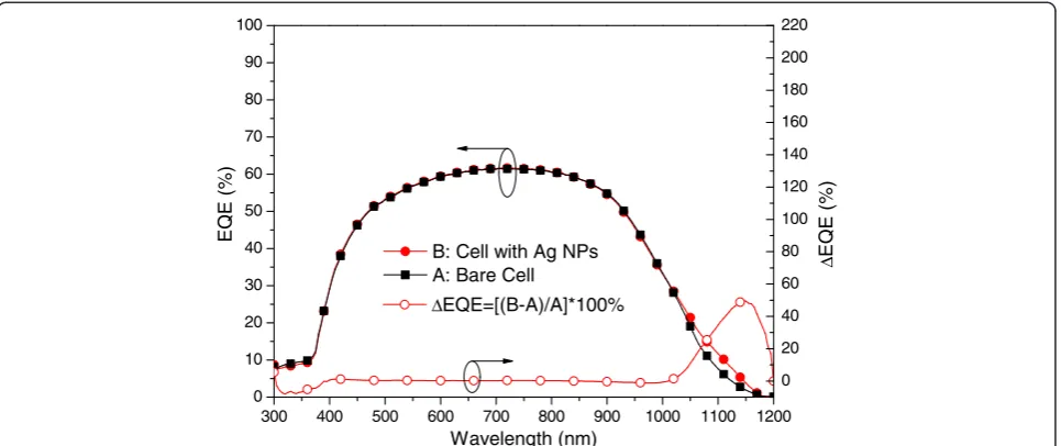
Figure 7EQE of the bare solar cell (sample A) and cell with Ag NPs (sample B).
0.0 0.1 0.2 0.3 0.4 0.5 0.6
0.0 0.5 1.0 1.5 2.0 2.5 3.0 3.5 4.0 4.5
C
u
rr
ent
(m
A
)
Voltage (V) C: Cell with Ag NPs and TiO2
B: Cell with Ag NPs
Figure 8Photovoltaic I-V curves of plasmonic solar cells of sample B and C.Sample B: the cell with Ag NPs on the rear surface, Sample C: the cell with a 30 nm-thick TiO2spacing layer on
[image:4.595.305.540.516.685.2]deposition of metallic nanoparticles on the front and rear surfaces at wavelengths of between 300 and 1,200 nm. Besides, the increased EQE leading to pro-moteJscand ηis also revealed in this study step by step
due to Jsc proportional to EQE and η proportional to
Jsc×Voc.
[image:5.595.58.538.88.292.2]Photovoltaic I-V and EQE response of plasmonic solar cell with Ag NPs on the rear surface
Figure 6 presents the photovoltaic I-V curves of a bare solar cell (sample A) and a plasmonic solar cell with Ag NPs on the rear surface (sample B). Under one sun AM 1.5 G illumination, the bare solar cell has an Isc of
2.98 mA, an open-circuit voltage (Voc) of 0.53 V, and an
ηof 9.81%. In contrast, the plasmonic solar cell with Ag NPs on the rear surface presented an Isc of 3.09 mA, a
Vocof 0.53 V, andηof 10.18%. The improvements inIsc
(3.69%) andη(3.77%) can be attributed to the plasmonic scattering produced by the Ag NPs on the rear surface. Figure 7 presents the EQE response of samples A and B. We observed a peak EQE enhancement (ΔEQE) of 50% at a wavelength of 1,150 nm andΔEQE bandwidth from 1,050 to 1,190 nm, compared with the results obtained from a bare solar cell. Thus, the increase inIsccan be
at-tributed to the plasmonic scattering of Ag NPs at long wavelengths, as confirmed by EQE measurements.
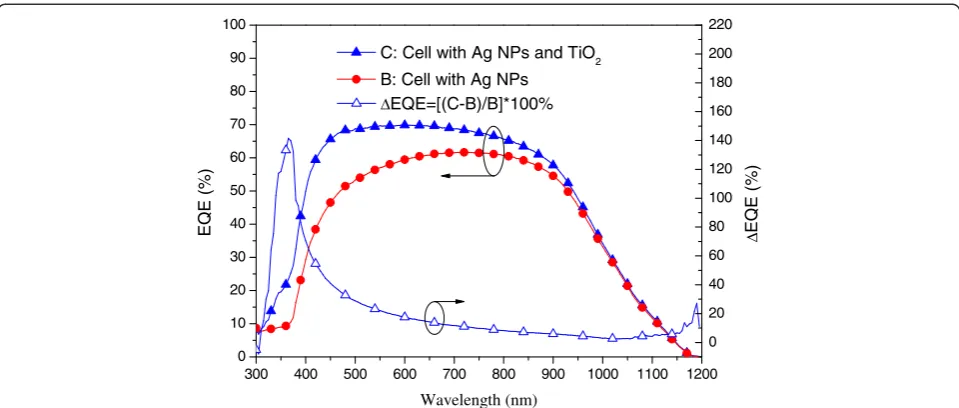
Photovoltaic I-V and EQE response of plasmonic solar cell with TiO2spacing layer on the front surface
Figure 8 presents the photovoltaic I-V curves of a plas-monic solar cell with Ag NPs and an Al-electrode on the rear surface (sample B) as well as that of a plasmonic solar cell with a 30 nm-thick TiO2spacing layer on the
front surface (sample C). Under one sun AM 1.5 G illu-mination, sample C presented anIscof 3.63 mA, aVocof
0.53 V, and an η of 11.91%. The improvements in Isc
(11.50%) andη(16.99%) can be attributed to a reduction in the reflective loss from the surface of the solar cell due to the antireflective properties of the TiO2 layer.
Figure 9 presents the EQE response of samples B and C. An EQE enhancement (ΔEQE) of >20% was observed at wavelengths between 350 and 750 nm and high EQE values (>60%) at shorter wavelengths due to a reduction 300 400 500 600 700 800 900 1000 1100 1200
0 10 20 30 40 50 60 70 80 90 100
Δ
EQE
(%)
EQE
(%)
Wavelength (nm)
C: Cell with Ag NPs and TiO2
B: Cell with Ag NPs
0 20 40 60 80 100 120 140 160 180 200 220
ΔEQE=[(C-B)/B]*100%
Figure 9EQE response of plasmonic solar cells of sample B and C.Sample B: the cell with Ag NPs on the rear surface, Sample C: the cell with a 30 nm-thick TiO2spacing layer on the front surface.
0.0 0.1 0.2 0.3 0.4 0.5 0.6
0.0 0.5 1.0 1.5 2.0 2.5 3.0 3.5 4.0 4.5
Cu
rre
n
t
(mA)
Voltage (V) D: Cell with Ag NPs and In NPs/TiO
2 B: Cell with Ag NPs
Figure 10Photovoltaic I-V curves of plasmonic solar cells of sample B and D.Sample B: the cell with Ag NPs on the rear surface, Sample D: the cell with In NPs/TiO2on the front surface as
well as Ag NPs on the rear surface.
Hoet al. Nanoscale Research Letters2014,9:483 Page 5 of 8
[image:5.595.304.539.516.685.2]in reflective loss due to the 30-nm TiO2 layer on the
surface of the solar cell.
Photovoltaic I-V and EQE response of plasmonic thin sili-con solar cell with In NPs/TiO2layer on the front surface and Ag NPs on the rear surface
Figure 10 presents the photovoltaic I-V curves of a plas-monic solar cell with Ag NPs on the rear surface (sample B) and a plasmonic solar cell with In NPs/TiO2 on the
front surface as well as Ag NPs on the rear surface (sam-ple D). Under one sun AM 1.5 G illumination, sam(sam-ple D presented anIscof 3.93 mA, aVocof 0.54 V, and anηof
13.02%. The improvements inIsc(27.18%) andη(27.90%)
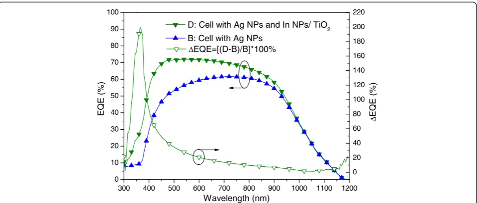
can be attributed to the plasmonic scattering of In NPs on the front surface and Ag NPs on the rear surface. Figure 11 presents the EQE response of samples B and D. A large EQE enhancement (ΔEQE >70%) was observed at wave-lengths of between 350 and 400 nm, and a considerable increase in EQE compared with sample B was observed at shorter wavelengths due mainly to the scattering effects of In NPs. We can therefore attribute the increase inIscto
the plasmonic scattering of In NPs at shorter wavelengths, which exceeded that of the Ag NPs at long wavelengths. Figure 12 and Figure 13, respectively, present the photo-voltaic I-V curves and EQE response of the bare solar cell and plasmonic solar cell with In NPs on the front surface and Ag NPs on the rear surface. Overall,Iscwas enhanced
by 31.59% and η was enhanced by 32.72%, compared to the bare solar cell. Besides, Figure 14 shows In NPs contri-bution to EQE which exhibited EQE enhancement of
>20% between 300 and 400 nm wavelengths, compared to sample C. Table 1 summarizes the photovoltaic perform-ance of samples A, B, C, and D.
Conclusions
This study fabricated and characterized thin silicon solar cells with different metallic nanoparticles deposited on the front and rear surfaces. The EQE response revealed plas-monic scattering at short wavelengths by the In NPs on the front surface and at long wavelengths by the Ag NPs 300 400 500 600 700 800 900 1000 1100 1200
0 10 20 30 40 50 60 70 80 90 100
Δ
EQE
(%)
EQE
(%)
Wavelength (nm)
D: Cell with Ag NPs and In NPs/ TiO2
B: Cell with Ag NPs
0 20 40 60 80 100 120 140 160 180 200 220
[image:6.595.59.539.88.293.2]ΔEQE=[(D-B)/B]*100%
Figure 11EQE responses of plasmonic solar cells of sample B and D.Sample B: the cell with Ag NPs on the rear surface, Sample D: the cell with In NPs/TiO2on the front surface as well as Ag NPs on the rear surface.
0.0 0.1 0.2 0.3 0.4 0.5 0.6
0.0 0.5 1.0 1.5 2.0 2.5 3.0 3.5 4.0 4.5
Cu
rre
n
t
(mA)
Voltage (V) D: Cell with Ag NPs and In NPs/TiO
[image:6.595.305.538.524.694.2]2 A: Bare Cell
300 400 500 600 700 800 900 1000 1100 1200 0
10 20 30 40 50 60 70 80 90 100
Δ
EQE
(%)
EQE
(%)
Wavelength (nm)
D: Cell with Ag NPs and In NPs/TiO2
A: Bare Cell
0 20 40 60 80 100 120 140 160 180 200 220
[image:7.595.57.539.88.294.2]ΔEQE=[(D-A)/A]*100%
Figure 13EQE responses of sample A and D.Sample A: the bare solar cell, Sample D: the cell with In NPs on the front surface and Ag NPs on the rear surface.
300 400 500 600 700 800 900 1000 1100 1200 0
10 20 30 40 50 60 70 80 90 100
Δ
EQE
(%)
EQE
(%)
Wavelength (nm)
D: SC w/rear Ag NPs+front TiO230 nm/In NPs
C: SC w/rear Ag NPs+front TiO230 nm
-10 0 10 20 30 40 50 60 70 80 90 100
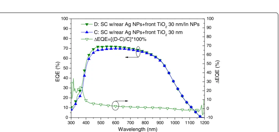
[image:7.595.62.540.339.566.2]ΔEQE=[(D-C)/C]*100%
Figure 14In NPs contribution to EQE.Which exhibited EQE enhancement of >20% between 300 and 400 nm wavelengths, compared to sample C.
Table 1 Summary of photovoltaic performance of samples A, B, C, and D
Isc(mA) Voc(V) η(%) ΔIsc(%) Δη(%)
A: Bare cell 2.98 0.53 9.81
B: Cell with Ag NPs 3.09 0.53 10.18 3.69 3.77
C: Cell with Ag NPs and TiO2 3.63 0.53 11.91 17.50 16.99
D: Cell with Ag NPs and In NPs/TiO2 3.93 0.54 13.02 8.32 9.31
Enhancement (D-B/B) × 100 27.18 27.90
Enhancement (D-A/A) × 100 31.59 32.72
Hoet al. Nanoscale Research Letters2014,9:483 Page 7 of 8
[image:7.595.56.539.635.733.2]on the rear side. Overall improvements in short-circuit current and conversion efficiency were in strong agree-ment with the EQE response resulting from the broad-band plasmonic scattering produced by the different metallic NPs on each surface.
Competing interests
The authors declare that they have no competing interests.
Authors’contributions
The work presented here was performed in collaboration of all authors. WJH figured out the mechanism about this research, participated in the analysis of data, and organized the article. YYL and SYS did the solar cells fabrication and SEM, photovoltaic I-V, and EQE measurements. All authors read and approved the final manuscript.
Acknowledgements
The authors would like to thank the National Science Council of the Republic of China for financial support under Grant NSC-100-2221-E-027-053-MY3.
Received: 26 June 2014 Accepted: 5 September 2014 Published: 11 September 2014
References
1. Harry AA, Albert P:Plasmonics for improved photovoltaic devices. Nat Mater2010,9:205.
2. Pillai S, Green MA:Plasmonics for photovoltaic applications.Sol Energy Mater Sol Cells2010,94:1481.
3. Adamovic N, Schmid U:Potential of plasmonics in photovoltaic solar cells.Elektrotechnik Informationstechnik2011,128:342.
4. Green MA, Pillai S:Harnessing plasmonics for solar cells.Nat Photonics 2012,6:130.
5. Stuart HR, Hall DG:Island size effects in nanoparticle-enhanced photodetectors.Appl Phys Lett1998,73:3815.
6. Keely KL, Coronado E, Zhao LL, Schatz GC:The optical properties of metal nanoparticles: the influence of size, shape, and dielectric environment. J Phys Chem2003,B107:668.
7. Xu G, Tazawa M, Jin P, Nakao S, Yoshimura K:Wavelength tuning of surface plasmon resonance using dielectric layer on silver island films. Appl Phys Lett2003,82:3811.
8. Temple TL, Mahanama DDK, Reehal HS, Bagnall DM:Influence of localized surface plasmon excitation in silver nanoparticles on the performance of silicon solar cells.Sol Energy Mater Sol Cells2009,93:1978.
9. Ghosh SK, Pal T:Interparticle coupling effect on the surface plasmon resonance of gold nanoparticles: from theory to applications.Chem Rev 2007,107:4797.
10. Beck FJ, Mokkapati S, Catchpole KR:Plasmonic light-trapping for Si solar cells using self-assembled Ag nanoparticles.Prog Prog Photovol2010, 18:500.
11. Merterns H, Verhoeven J, Polman A, Tichelaar FD:Infrared surface plasmon in two-dimensional silver nanoparticle arrays in silicon.Appl Phys Lett 2004,85:1317.
12. Lee S, Lee M, Shin H, Choi D:Control of density and LSPR of Au nanoparticles on grapheme.Nanotechnology2013,24:275702. 13. Yang Y, Pillai S, Mehrvarz H, Kampwerth H, Ho-Baillie A, Green MA:
Enhanced light trapping for high efficiency crystalline solar cells by the applications of rear surface plasmons.Sol Energy Mater Sol Cells2012, 101:217.
14. Anno E, Tanimoto M:Size-dependent change in interbank absorption and broadening of optical plasma-resonance absorption of indium particles.J Appl Phys2005,98:053510.
15. Lee YY, Ho WJ, Liu JJ, Lin CH:Light-trapping performance of silicon thin-film plasmonics solar cells based on indium nanoparticles and various TiO2layer thickness.J J Appl Phys2014,53:06JE11.
doi:10.1186/1556-276X-9-483
Cite this article as:Hoet al.:External quantum efficiency response of thin silicon solar cell based on plasmonic scattering of indium and silver nanoparticles.Nanoscale Research Letters20149:483.
Submit your manuscript to a
journal and benefi t from:
7 Convenient online submission 7 Rigorous peer review
7 Immediate publication on acceptance 7 Open access: articles freely available online 7 High visibility within the fi eld
7 Retaining the copyright to your article