
N A N O E X P R E S S
Open Access
Small-area and compact CMOS emulator circuit
for CMOS/nanoscale memristor co-design
SangHak Shin
1, Jun-Myung Choi
1, Seongik Cho
2and Kyeong-Sik Min
1*Abstract
In this paper, a CMOS emulator circuit that can reproduce nanoscale memristive behavior is proposed. The proposed emulator circuit can mimic the pinched hysteresis loops of nanoscale memristor memory's current-voltage relationship without using any resistor array, complicated circuit blocks, etc. that may occupy very large layout area. Instead of using a resistor array, other complicated circuit blocks, etc., the proposed emulator circuit can describe the nanoscale memristor's current-voltage relationship using a simple voltage-controlled resistor, where its resistance can be programmed by the stored voltage at the state variable capacitor. Comparing the layout area between the previous emulator circuit and the proposed one, the layout area of the proposed emulator circuit is estimated to be 32 times smaller than the previous emulator circuit. The proposed CMOS emulator circuit of nanoscale memristor memory will be very useful in developing hybrid circuits of CMOS/nanoscale memristor memory.
Keywords: Emulator circuit; CMOS emulator circuit; Memristors; Memristive behavior; Nanoscale memristor memory; CMOS/nanoscale memristor co-design
Background
Memristors are being intensively explored as possible candidate for future memories because of simplicity in fabrication, possibility in three-dimensional integra-tion, compatibility with (complementary metal-oxide-semiconductor) CMOS technology in the fabrication process, and so on. However, real integration of mem-ristors and CMOS circuits is very rarely available to most engineers and scholars who want to be involved in designing various kinds of CMOS circuits using memristors. To help those engineers and scholars who cannot access memristor fabrication technology but want to design memristor circuits, a CMOS emu-lator circuit that can reproduce the physical hyster-esis loop of memristor's voltage-current relationship is needed.
Methods
Before we develop a CMOS emulator circuit for memris-tor, memristive behavior should be explained first. The
following simple equation (Equation 1) can describe the memristor's current-voltage relationship [1,2]:
v tð Þ ¼RXð Þt ⋅i tð Þ ¼ RSETw tDð ÞþRRESET 1−w tDð Þ
i tð Þ
¼ RSETQq tð Þ
CRITþRRESET
1− q tð Þ
QCRIT
i tð Þ where
w tð Þ
D ¼μvRDSET2 q tð Þ ¼
q tð Þ
QCRIT; and QCRIT ¼
D2
μvRSET
ð1Þ Here v(t) and i(t) represent the voltage and current of memristor, respectively. RX(t) is the memristance that changes with respect to time.RSETandRRESETare SET and
RESET resistance, respectively. w(t) is the effective width of the memristor.Dis the total drift length ofw(t).q(t) is an accumulated charge flow through the memristor.QCRIT
means an amount of critical charge to RESET-to-SET transition. When q(t) becomes equal to QCRIT, RX(t) is
changed to RSETfrom RRESET. Here μv is the mobility of dopant in Equation 1 [1,2].
To describe the memristive behavior that follows the relationship of current and voltage in Equation 1, a few emulator circuits have already been proposed [3-5].
* Correspondence:[email protected]
1School of Electrical Engineering, Kookmin University, Seoul 136-702, Korea
Full list of author information is available at the end of the article
Pershin and Ventra proposed an emulator circuit that is composed of an analog-to-digital converter and micro-controller that are implemented by discrete off-chip de-vices. Thus, they can be considered too much complicated and too large to be integrated in a single chip [3]. Jung et al. proposed an emulator circuit that is based on CMOS technology [4], where a memristor that should change its resistance in response to the applied current and voltage is implemented by an array of resistors. In the emulator circuit with resistor array, the analog-to-digital converter and the decoder circuit select a proper resistor among many resistors that are placed in the resistor array according to the applied voltage or current [4]. One problem in the emulator circuit [4] is that the voltage-current relationship seems sawtooth. This is because the resolution of memristance change is decided by the resolution of the analog-to-digital converter, as you see in [4]. If we have 4-bit analog-to-digital converter in the emulator circuit, it means that only 16 values of memristance are available. As a result, when we apply a voltage that is a sinusoidal function to the memristor, we can know that its current is increased or decreased like sawtooth. To improve the resolution of memristance change, the resolution of the analog-to-digital converter should be increased too. If the resolution of the analog-to-digital converter is improved from 4 to 5 bit, the voltage-current relationship of the emulator circuit with 5 bit seems to be much finer than the emulator circuit with a 4-bit analog-to-digital converter, as shown in [4]. To improve the resolution twice, however, the number of resistors in the resistor array should be double too. It can cause a large area overhead in realizing this emulator circuit in a single chip. Especially, in implementing memristor array with this emulator circuit, this large area overhead of each memristor emulator cell can be a serious problem because each cell in the memristor array should be realized by this large-area single memristor emulator.
To mitigate the large area overhead of the previous emulator circuit, we propose a new emulator circuit of memristors that is more compact and simpler than the previous emulator circuits [6]. The new emulator circuit does not use a resistor array, an analog-to-digital converter, and so on that usually occupy very large area. Instead of using the complicated circuit blocks that were mentioned just earlier, the new circuit can change its memristance value by a simple voltage-controlled resistor that can be realized by a single n-type metal-oxide-semiconductor field-effect transistor (NMOSFET) device.
Newly proposed emulator circuit for describing memristive behavior
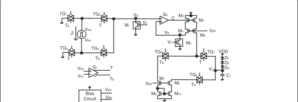
A schematic of the proposed emulator circuit for describ-ing memristive behavior is shown in Figure 1. The CMOS circuit for emulating memristive behavior is composed of transmission gates, comparators, current mirrors, voltage-controlled resistor, etc. as shown in Figure 1.VINis an
in-put voltage source andVIN+andVIN−represent the anode
and cathode of the input voltage source, respectively. In Figure 1,VIN+is connected to TG1and TG2that are
controlled by TBand T, respectively. Similarly,VIN− is
connected to TG3 and TG4 that are controlled by T
and TB, respectively. When VIN+ is greater than VIN−, T
becomes high and TB becomes low, by the comparator
G1. On the contrary, when VIN+ is smaller than VIN−, T
becomes low and TBbecomes high. Thus, we can know
that VIN+ is connected to VA through TG2when VIN+
is larger than VIN−. At the same moment,VIN− is
con-nected to the ground potential (GND) by TG3. When
VIN− is larger than VIN+, VIN− is connected to VA
through TG4, andVIN+is biased by GND through TG1.
One thing to note here is that we can deliver the input voltage VIN to VA without any sacrificial voltage loss,
using the transmission gate.
VBP VA
. VC
VC
VIN-VIN+ VC
VBN .
. . .
. VB
C
I
IN
G2
C1 M3
M5
M4
M6 M1
M2
M7
M8
M9
M10
D3 T
TB G1
T
T
TG2
TG4 TG3
TG1
TB TB
TB
TB T
TG7
TG6 TG5
Bias Circuit
VBP
VBN VIN+
[image:2.595.56.539.547.713.2]D2 D1 VDD
The VIN delivering block that is composed of four
transmission gates, TG1, TG2, TG3, and TG4, can deliver VIN+and VIN− that are plus and minus polarity of VIN,
respectively, toVAthat has only plus polarity, not minus.
The delivered voltage VAis copied exactly to VB by the
negative feedback circuit that is composed of the OP amp, G2, M3, and M4. Using this circuit block,VBcan
be the same asVAby the feedback amplifier with unity
gain.VBis connected to the voltage-controlled resistor
M2 that is controlled by VC. One more thing to note
here is that VC controls both voltage-controlled
resis-tors M1and M2that are electrically isolated from each
other. By doing so, we can separate the memristor's current from the programming current to change the state variable that is stored at the capacitor C1. If the
memristor's current is not separated from the program-ming current, the state variable that decides memristance value can be maintained only at the moment when the programming voltage or current is applied to the memristor. If so, the emulator circuit cannot keep its
(a)
(c) (b)
(d)
(e)
(f)
(g)
(h) 0.25[msec]
0.20 0.25 0.30
-2 0 2
f=10kHz
V
IN
[V
]
Time [msec]
0.20 0.25 0.30
1 2 3
V
C
[V
]
Time [msec]
0.20 0.25 0.30
-100 0 100
I
IN
[
A
]
Time [msec]
0.30 0.35 0.40 0.45
-2 0 2
V
IN
[V
]
Time [msec] f=40kHz
0.30 0.35 0.40 0.45
-100 0 100
I
IN
[
A
]
Time [msec]
0.30 0.35 0.40 0.45
1 2 3
V
C
[V
]
Time [msec]
-2 -1 0 1 2
-100 -50 0 50 100
VDD=3.3V f=10kHz
Memristor current[
A]
Memristor voltage[V]
-2 -1 0 1 2
-100 -50 0 50 100
Memristor current
[
A
]
Memristor voltage[V] VDD=3.3V
[image:3.595.60.537.223.686.2]f=40kHz
Figure 2Simulated voltage waveforms.The simulated voltage waveforms of(a)VIN,(b)IIN,(c)VC, and(d)the pinched hysteresis loop of the
voltage-current relationship of the proposed emulator circuit when the sinusoidal frequency is 10 kHz. The simulated voltage waveforms of(e)
VIN,(f)IIN,(g)VC, and(h)the pinched hysteresis loop of the voltage-current relationship of the proposed emulator circuit when the sinusoidal
programmed state variable when the applied voltage or current is removed.
VC that controls two voltage-controlled resistors M1
and M2 acts as a state variable in the emulator circuit
that is calculated by an amount of stored charge at C1.
When VIN+ is greater than VIN−, TG7 is on and both
TG5and TG6are off. At this time, the current mirror that
is composed of M5 and M6 delivers the programming
current to C1 to increase an amount of stored charge;
thereby the state variable becomes larger. On the other hand, whenVIN−is greater thanVIN+, TG7is off and both
TG5and TG6are on. By doing so, we can decrease the
amount of charge that is stored at the state variable capacitorC1. The discharging current path is composed
of M7, M8, M9, and M10in Figure 1. Here VBN andVBP
are the biasing voltages for NMOSFETs and PMOSFETs,
respectively. VBN and VBP are made from the biasing
circuit that is shown in Figure 1. D1, D2, and D3are the
diodes that are used in the proposed emulator circuit to
limit the minimum value ofVC. This minimum value of
VCis needed to avoid the dead zone which may be caused
by the sub-threshold region of the voltage-controlled resistors M1and M2.VD means the diode voltage of D1,
D2, and D3.VDDis the power supply voltage of the CMOS
emulator circuit in Figure 1.
One more thing to consider here is that the nonlinearity of memristive behaviors can be found when the effective
width of memristor, w(t), in Equation 1 becomes much
closer to the boundary constraints [1,7]. This nonlinearity near the boundary values of w(t) was introduced in the HP model [1] and mathematically modeled by Corinto and Ascoli [7] to describe various nonlinear behaviors of memristors. In terms of implementation, the diode bridge circuit with LCR filter was proposed to reproduce mem-ristive nature with nonlinearity by using a very simple electronic circuit [8]. In this paper, the window function that is used to define two boundary values of the state variable in the HP model [1] is realized in the CMOS emulator circuit that is shown in Figure 1. The emulator circuit in Figure 1 has two boundary values of the state variable that is defined byVC. Here we can know that the
maximum value of VC cannot exceedVDD. And also,VC
cannot be lower thanVDD-3VD. Thus, the state variable of VCin Figure 1 can exist only betweenVDDandVDD-3VD,
not being higher than VDD and lower than VDD-3VD,
respectively.
Results and discussion
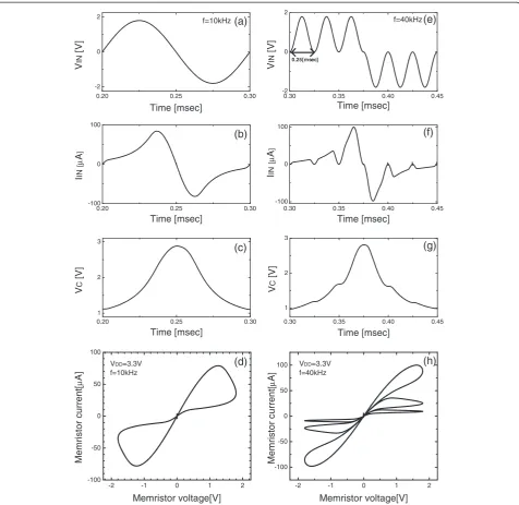
Figure 2a shows the applied input voltage,VIN, to the
proposed circuit for emulation of memristive behavior. The voltage waveform is sinusoidal and its frequency and magnitude are 10 kHz and 1.8 V, respectively. The mem-ristor's currentIINthat is emulated by the proposed circuit
in Figure 1 is shown in Figure 2b. As the sinusoidal
voltage is applied to the emulator circuit in Figure 1, IINchanges with respect to time according to the state
variable that is represented by VC, the amount of stored
charge at C1. WhenVChas the lowest value, it means that
the state variable is in RESET state, where the emulator circuit acts like a memristor with RESET resistance. After the half cycle of sinusoidal function,VC is charged more
and more; thereby VC can reach the highest value. With
the highest value of VC, the state variable can be in SET
state, where the emulator circuit can be considered a SET
(a)
(b)
(c)
0.0 0.4 0.8 1.2
0 1 2 3
SET pulse [V]
Time [msec]
0.0 0.4 0.8 1.2
0 1 2 3
RESET pulse [V]
Time [msec]
0.0 0.4 0.8 1.2
0 1 2 3
Vc
[V]
Time [msec]
RESET
SET
[image:4.595.306.537.228.683.2]Partial states
Figure 3The simulation results of partial states between‘SET’ state and‘RESET’state. (a)The voltage waveform of the SET pulse,
resistance. Figure 2c shows the voltage waveform of VC
with respect to time. At the starting point of sinusoidal function of VIN,VC is 1.2 V that is decided by D1 in
Figure 1. After the half cycle of sinusoidal function,VC
reaches 2.8 V. When one cycle of sinusoidal function is
completed, the VC value returns to the value at the
[image:5.595.59.540.237.693.2]starting point of sinusoidal function. Figure 2d shows a typical pinched hysteresis loop of a memristor's voltage and current which are emulated by the proposed circuit in Figure 1. In the simulation,VDDis 3.3 V and the frequency
of sinusoidal function is 10 kHz.
Figure 2e, f, g, h shows the simulation results of the pro-posed emulator circuit with four times higher frequency of 40 kHz than that of Figure 2a, b, c, d,VIN,IIN,VC, and
the pinched hysteresis loop, respectively, with 10 kHz. A sinusoidal voltage with 40 kHz that is applied to the emulator circuit is shown in Figure 2e. Here the first three peaks are for increasing VC in Figure 1; thereby,
the emulator circuit changes from RESET to SET. The next three peaks are for decreasing the state variable; thus, the emulator circuit can return to RESET.IINandVCwith
the sinusoidal function that is indicated in Figure 2e are
VREF
DOUT
RD RDB
Read circuit
Write driver
. M1
M2
M3 .
. .
RD M4
M5
TG1 .
. DIN
anode
cathode
.
.
(a)
(b)
RD
RD
WR
WR TG2
TG3
TG4
0.00 0.01 0.02 0.03 0.04 0.05
0 2 4
D
OUT
[V]
Time [msec]
0.00 0.01 0.02 0.03 0.04 0.05
0 2 4
D
IN
[V]
Time [msec]
0.00 0.01 0.02 0.03 0.04 0.05
0 2 4
RD [V]
Time [msec]
0.00 0.01 0.02 0.03 0.04 0.05
0 2 4
WR [V]
Time [msec]
VSEN
G1 G2
G3 G4
Figure 4The read and write circuits for the proposed emulator circuit of memristors and the simulated voltage waveforms. (a)The read and write circuits for the proposed emulator circuit of memristors.(b)The simulated voltage waveforms ofDIN, WR, RD, andDOUTthat are
shown in Figure 2f, g, respectively. Figure 2h shows the voltage-current relationship of the emulator circuit. In Figure 2h we can see three voltage-current loops at the right and another three voltage-current loops at the left which correspond to the three high peaks and three low peaks in Figure 2e, respectively.
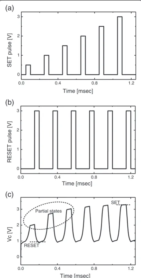
Figure 3a shows SET pulses with different amplitude values. Here the amplitude values are increasing mono-tonically from 0.5 to 3 V. Each SET pulse is followed by a RESET pulse with the fixed amplitude as high as 3 V that is shown in Figure 3b. The state variable that is changed by
SET and RESET pulses are shown in Figure 3c. Here VC
represents the amount of stored charge at C1that controls
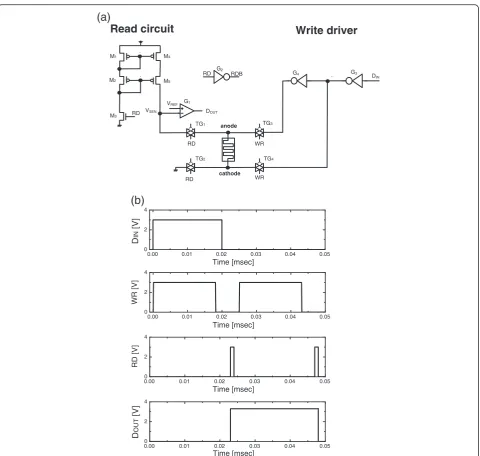
the voltage-controlled resistor in Figure 1 that acts as memristor. Figure 4a shows the read and write circuits for the proposed emulator circuit of memristors [9,10]. The read circuit is simply composed of a current mirror and
comparator. The comparator G1 compares the sensing
voltageVSENwith the reference voltageVREF. The sensing
voltage VSEN can change according to the programmed
memristance value of the emulator circuit. If the state
variable is closer to RESET, the sensing voltage VSEN
becomes larger due to a large value of memristance. On the contrary, the state variable is in SET, andVSENis
smaller thanVREF. HereDOUTis the output voltage of the
read circuit. G2 is the inverter for RD that is the ‘read’
command signal. TG1and TG2are the transmission gates
for the read operation. When RD is high, TG1 and TG2
are on. On the contrary, TG3 and TG4 are on for the
‘write’ operation that is activated by the write command signal WR. The input dataDINdrives the inverter G3. And
G3drives the next inverter G4. The anode and cathode
of the proposed emulator circuit are driven by the two inverters, G3and G4, respectively. Figure 4b shows the
voltage waveforms ofDIN, WR, RD, andDOUT.
Figure 5 compares the layout area of the previous emulator circuit [4] and the proposed emulator circuit.
Because the resistor array is not used in the proposed circuit and the analog-to-digital converter and decoder are eliminated in this paper, the layout area of the previous emulator circuit is estimated to be 32 times larger than the emulator circuit proposed in this paper. The design rule used in this layout is MagnaChip 0.35-μm technology.
Conclusions
In this paper, a CMOS circuit that could emulate memris-tive behavior was proposed. The proposed emulator circuit could mimic the pinched hysteresis loops of a memristor's current-voltage relationship without using a resistor array and complicated circuit blocks that may occupy very large layout area. Instead of using a resistor array, other complicated circuit blocks, etc., the proposed emulator circuit could mimic memristive behavior using simple voltage-controlled resistors, where the resistance can be programmed by the stored voltage at the state variable capacitor. Comparing the layout area between the previous emulator circuit and the proposed one, the layout area of the emulator circuit proposed in this paper was estimated to be 32 times smaller than the previous emulator circuit.
Competing interests
The authors declare that they have no competing interests.
Authors’contributions
All authors have contributed to the submitted manuscript of the present work. KSM defined the research topic. SHS and JMC did the simulation and layout. SC provided critical comments on the draft manuscript. KSM wrote the paper. All authors read and approved the final manuscript.
Authors’information
SHS and JMC are M.S. students who are studying at the School of Electrical Engineering, Kookmin University, Seoul, Korea. SC is a professor at the Division of Electronics and Information Engineering, Chonbuk National University, Jeonju, Korea. KSM is a professor at the School of Electrical Engineering, Kookmin University, Seoul, Korea.
The previous emulato rcircuit
1,400 mm
1,000mm
280mm
160 mm Area:
32x vs.1x
1X
32X
[image:6.595.59.540.89.248.2]The propose done
Acknowledgements
This work was financially supported by the SRC/ERC program (R11-2005-048-00000-0), the Basic Science Research Program (2010–0023469), the Global Research Network Program (NRF-2011-220-D00089), the Nano-Material Technology Development Program (2011–0030228), and
NRF-2013K1A3A1A25038533 through the National Research Foundation of Korea (NRF) funded by the Ministry of Science, ICT & Future Planning, and the Industrial Strategic Technology Development Program funded by the Ministry of Trade, Industry and Energy (MOTIE, Korea) (10039239). The CAD tools were supported by the IC Design Education Center (IDEC), Korea.
A part of this work was presented at the Collaborative Conference on 3D & Materials Research (CC3DMR), Jeju, Korea, in June 2013.
Author details
1School of Electrical Engineering, Kookmin University, Seoul 136-702, Korea. 2
Division of Electronics and Information Engineering, Chonbuk National University, Jeonju 561-756, Korea.
Received: 16 July 2013 Accepted: 4 September 2013 Published: 1 November 2013
References
1. Strukov DB, Snider GS, Stewart DR, Williams RS:The missing memristor found.Nature2008,453:80–83.
2. Jo KH, Jung CM, Min KS, Kang SM:Memristor models and circuits for controlling Process-VDD-Temperature variations.IEEE Trans Nanotechnol
2010,9(6):675–678.
3. Pershin YV, Ventra MD:Practical approach to programmable analog circuits with memristors.IEEE Trans Circuits Syst-I2010,57(8):1857–1864. 4. Jung CM, Jo KH, Min KS:SPICE macromodel and CMOS emulator for
memristors.J Nanosci Nanotechnol2012,12(2):1487–1491.
5. Kim H, Sah MP, Yang C, Cho S:Memristor emulator for memristor circuit applications.IEEE Trans Circuits and Syst-I2012,59(10):2422–2431. 6. Choi JM, Shin SH, Cho SI, Min KS:CMOS circuit with small area and low
complexity for emulating memristive behavior. InCollaborative Conference on 3D & Materials Research (CC3DMR).Jeju in Korea; 2013.
7. Corinto F, Ascoli A:A boundary condition-based approach to the modeling of memristor nano-structures.IEEE Trans Circuits and Syst-I2012, 59(11):2713–2726.
8. Corinto F, Ascoli A:Memristive diode bridge with LCR filter.Electronics Letters2012,48(14):824–825.
9. Lee KJ, Cho BK, Cho WY, Kang S, Choi BG, Oh HR, Lee CS, Kim HJ, Park JM, Wang Q, Park MH, Ro YH, Choi JY, Kim KS, Kim YR, Shin IC, Lim KW, Cho HK, Choi CH, Chung WR, Kim DE, Yoon YJ, Yu KS, Jeong GT, Jeong HS, Kwak CK, Kim CH:A 90 nm 1.8 V 512 Mb diode-switch PRAM with 266 MB/s read throughput.IEEE J Solid-State Circuits2008,43(1):150–161.
10. Qureshi MS, Pickett M, Miao F, Strachan JP:CMOS interface circuits for reading and writing memristor crossbar array. InIEEE International Symposium on Circuits and Systems (ISCAS): 15–18 May 2011; Rio de Janeiro.
Piscataway: IEEE; 2011:2954–2957.
doi:10.1186/1556-276X-8-454
Cite this article as:Shinet al.:Small-area and compact CMOS emulator circuit for CMOS/nanoscale memristor co-design.Nanoscale Research Letters
20138:454.
Submit your manuscript to a
journal and benefi t from:
7 Convenient online submission
7 Rigorous peer review
7 Immediate publication on acceptance
7 Open access: articles freely available online
7 High visibility within the fi eld
7 Retaining the copyright to your article
![Figure 5 Comparison of layout area between the previous emulator circuit [4] and the proposed emulator circuit](https://thumb-us.123doks.com/thumbv2/123dok_us/8864977.939771/6.595.59.540.89.248/figure-comparison-previous-emulator-circuit-proposed-emulator-circuit.webp)
