N A N O E X P R E S S
Open Access
3D simulation of morphological effect on
reflectance of Si
3
N
4
sub-wavelength structures for
silicon solar cells
Yiming Li
*, Ming-Yi Lee, Hui-Wen Cheng and Zheng-Liang Lu
Abstract
In this study, we investigate the reflectance property of the cylinder, right circular cone, and square pyramid shapes of silicon nitride (Si3N4) subwavelength structure (SWS) with respect to different designing parameters. In
terms of three critical factors, the reflectance for physical characteristics of wavelength dependence, the reflected power density for real power reflection applied on solar cell, and the normalized reflectance (reflected power density/incident power density) for real reflectance applied on solar cell, a full three-dimensional finite element simulation is performed and discussed for the aforementioned three morphologies. The result of this study shows that the pyramid shape of SWS possesses the best reflectance property in the optical region from 400 to 1000 nm which is useful for silicon solar cell applications.
1. Introduction
Silicon solar cell is one of the promising renewable energy technologies in order to relieve the impact of the climate change. In semiconductor-based solar cells, elec-tron-hole pairs are generated through absorption of impinging photons. Due to high refraction index of semiconductor materials, especially silicon, the incident sunlight power is largely reflected back, resulting in the reduction of light absorption and poor energy conver-sion efficiency. Antireflection coating (ARC) is mounted over absorption layers, resulting in three effects: (a) reduction in surface reflection, (b) increase in light absorption due to an increase in optical path length by diffraction, and (c) enhancement of internal reflection that reduces the amount of escaping light. Based on the theory of impedance matching, single layer (SLR) and multilayer of ARC are proposed for reduced reflectance property; however, the resulting reflectance spectra meet the demand only within a narrow spectral domain. Sub-wavelength structure’s (SWS) dimensions are much smaller than the wavelengths of light; therefore, using ARC on the surface of silicon solar cells can substan-tially reduce the reflectivity and improve the capability
of light trapping. It thus will achieve the enhanced effi-ciency according to our recent both numerical and experimental studies [1-3]. Compared with silicon solar cell with a SLAR, the efficiency of silicon solar cell with Si3N4 SWS is promising among various ARC layers in our recent work [4]. A rigorous coupled-wave analysis (RCWA) [1,5-7] has been reported to estimate the reflectance of Si3N4 SWS by approximating structural shapes with partitioned uniform homogeneous layers. RCWA is an exact solution of Maxwell’s equations for the electromagnetic diffraction by grating structures which is generally applicable for 2D plane with 1D peri-odicity; however, RCWA may suffer numerical difficul-ties in presence of evanescent orders and it requires a large amount of calculation for retaining several diffrac-tion orders. These factors limit flexible applicadiffrac-tion of RCWA; in particular, for 3D problems with non-azi-muthally symmetric structural shapes. Numerical simu-lation of 3D morphological effect on reflectance property has not been studied yet. Therefore, a full 3D finite-element (FE) analysis of Si3N4 SWS will be an interesting examination for quantitative understanding of the reflectance property.
In this study, 3D FE simulation for the reflectance of Si3N4 SWS with three types of structural shapes, the cylinder, the right circular cone, and the square pyramid shapes, is conducted with respect to different geometry * Correspondence: [email protected]
Parallel and Scientific Computing Laboratory, Department of Electrical Engineering, National Chiao Tung University, 1001 Ta-Hsueh Road, Hsinchu 300, Taiwan
parameters and lighting angles for quantitative under-standing of reflectance property. First, proper selection on the boundary conditions can alleviate the computa-tional load from simulating a holistic ARC. The reflec-tance of Si3N4 SWS on the silicon substrate is thus simulated using the 3D finite element method (FEM); consequently, in terms of three critical factors, the reflectance for physical characteristics of wavelength dependence, the reflected power density for real power
reflection applied on solar cell, and the normalized reflectance (reflected power density/incident power den-sity) for real reflectance applied on solar cell are calcu-lated and discussed for the aforementioned three morphologies. The analysis of reflectance spectrum with wide-angle incidences of electromagnetic wave and the average reflectance with various heights are presented. Besides, according to our recent study, which presented the optimal design parameters of Si3N4 SWS based on
2 x 2 array
1 x 1 array
Periodic Structure
2 x 2 array
1 x 1 array
Periodic Structure
(a)
W
s
h
Air
Si
3N
4SWS
W
d
Non-etched
Si
3N
4layer
Si substrate
s
W
s
h
Air
Si
3N
4SWS
W
d
Non-etched
Si
3N
4layer
Si substrate
s
h
Air
Si
3N
4SWS
W
W
s
d
Non-etched
Si
3N
4layer
Si substrate
h
Air
Si
3N
4SWS
W
W
s
d
Non-etched
Si
3N
4layer
Si substrate
h
Air
Si
3N
4SWS
W
W
s
d
Non-etched
Si
3N
4layer
Si substrate
h
Air
Si
3N
4SWS
W
W
s
d
Non-etched
Si
3N
4layer
Si substrate
[image:2.595.61.538.210.707.2](b) (c) (d)
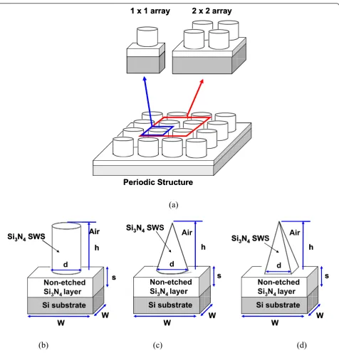
Figure 1(a) Plot of the periodic structure of Si3N4SWS with 1 × 1 and 2 × 2 arrays as unit cell. 3D schematic plots of the examined(b)
RCWA [4], numerical verification and comparison is accomplished following the discussion. The engineering findings of this study show that the pyramid shape of SWS possesses the best reflectance property in the opti-cal region from 400 to 1000 nm which is useful for sili-con solar cell applications.
This rest of the article is organized as follows. In Sec-tion 2, we show the computaSec-tional structure and model. In Section 3, we report the results and discussion. Finally, we draw conclusions and suggest future work.
2. The SWS and optical model
Based upon our experimental characterization, Figure 1a illustrates a periodical structure of Si3N4 SWS which is used in our 3D FE simulation without loss of generality. We study Si3N4SWS with the cylinder, the right circu-lar cone, and the square pyramid shapes, as shown in Figure 1b-d, respectively. With a constant volume, the diameter of cylinder- and right circular cone-shaped Si3N4 SWS and the edge length of square pyramid are 130 nm, the heights (h) of the etched part of Si3N4SWS are 200, 600, and 471.3 nm, the height (s) of the non-etched part is 70 nm, and the base (W) of a unit cell is 200 nm [4]. Note that the thickness of Si substrate is given 600 nm. Note that all structural parameters are adopted from our experimental studies [2-4,8]. Throughout the article, we consider time-harmonic fields assuming a time-dependence in e-jωt. The diffrac-tion problem is governed by the well-known Maxwell equations
∇ ×E=−jωμH, (1)
∇ ×H=J+jωεE, (2)
∇ ·E=ρ/ε, (3)
and
∇ ·B= 0, (4)
where E andD are electric field intensity and flux density, Hand B are magnetic field intensity and flux density, lis the corresponding frequency to the wave-lengthl, J, and rare current density and charge density, εis electric permittivity, μ is magnetic permeability. A repeated pattern is applicable to use periodic boundary conditions, thus the Floquet theorem is adopted to simulate the boundary condition of periodic structure. Floquet theorem asserts that the analysis region can be reduced significantly in one periodicity cell to character-ize the propagation property. The electric fields in peri-odic structure are related as follows:
E2(r)=E1
r+L=E1(r)e−jθ, (5)
where r is position vector,L is the distance between the periodic boundaries, and θis a phase factor deter-mined by wave vectorkandL:
θ =k·L, (6)
The polarization of transverse electric (TE) mode, in which the electric field is normal to the direction of wave propagation, is excited as the normal incident light source with wavelengths sweeping from 400 to 1000 nm. The bottom region of Si substrate is assigned as perfect matched layer in avoidance of reflected wave. The refraction index of Si3N4 is 2.05, and the refraction index of Si is frequency dependent with the relation [1]:
nSi=
ε+ A
λ2+
Bλ2
1
λ2−λ2
1
, (7)
wherelis the incident wavelength,A= 0.939816, B= 8.10461 × 10⁻³, l1 = 1.1071μm, and ε = 11.6858. The calculation settings of reflectance were reported and can be found in our recent studies [1,4].
3. Results and discussion
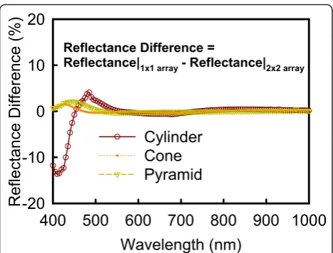
In order to examine the effect of Floquet boundary con-dition in 3D FE analysis, as shown in Figure 2, we com-pare the difference between the simulated unit cells of 1 × 1 and 2 × 2 array of Si3N4SWS. We find at the wave-lengths above 600 nm, the reflectance of 1 × 1 array of Si3N4 SWS as unit cell is almost consistent with unit cell of 2 × 2 array, meanwhile insignificant discrepancy
Wavelength (nm)
400 500 600 700 800 900 1000
Reflect
ance Differenc
e (%)
-20
-10
0
10
20
[image:3.595.305.539.494.672.2]Cylinder
Cone
Pyramid
Reflectance Difference =Reflectance|1x1 array - Reflectance|2x2 array
Figure 2Plot of the difference of reflectance spectrum of Si3N4
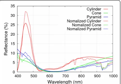
occurs at wavelengths shorter than 600 nm. Based on this consequence, it is enable us to do simulation with more computational efficient using 1 × 1 array of Si3N4 SWS as a simulated unit cell with engineering accepta-ble accuracy. According to our recent RCWA work [4], the reflectance spectra are first plotted in Figure 3 using the optimal design parameters [1,4]. Also, the spectra calculated by a full 3D FE analysis with the same design parameters are indicated by dashed lines. For the cylin-der-shaped Si3N4 SWS, the reflectance spectra for RCWA and FE analysis are similar, but not agreed for the cone-shaped Si3N4 SWS due to existing evanescent orders along the top of structures. This comparison confirms the importance of 3D FEM simulation which is beyond the RCWA approach [4].
Figure 4a-c shows the reflectance spectra with incident angles of 0°, 15°, 30°, 45°, and 60° for the cylinder-, right circular cone-, and square pyramid-shaped Si3N4 SWS, respectively. For the normal incidence case, the lowest
Wavelength (nm)
400 500 600 700 800 900 1000
R
eflectanc
e (%)
0
5
10
15
20
25
30
RCWA: Cylinder RCWA: Cone FE: Cylinder FE: Cone
Figure 3Comparison of the reflectance spectra for the cone-and cylinder-shaped Si3N4SWS calculated by RCWA and 3D FE
analysis with the same design parameters.
Wavelength (nm)
400 500 600 700 800 900 1000
R
e
flec
ta
nc
e (%)
0 20 40 60 80
100 0 deg
15 deg 30 deg 45 deg 60 deg
(a)
Wavelength (nm)
400 500 600 700 800 900 1000
Re
flectan
ce (
%
)
0 20 40 60 80
100 0 deg
15 deg 30 deg 45 deg 60 deg
Wavelength (nm)
400 500 600 700 800 900 1000
R
e
flecta
nce
(
%
)
0 20 40 60 80
100 0 deg
15 deg 30 deg 45 deg 60 deg
[image:4.595.58.539.331.704.2](b) (c)
Figure 4Plots of the reflectance spectrum for the (a) cylinder- (b) circular-cone-, (c) and square-pyramid-shaped Si3N4SWS with
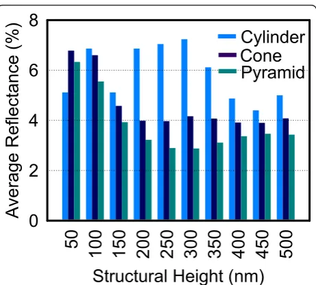
average reflectance among three structural shapes is 3.47% of square pyramid-shaped structure. The others are 6.86 and 4.42% for the cylinder- and the right cir-cular cone-shaped Si3N4 SWS, respectively. Meanwhile, as shown in Figure 4a-c, one can observe that the reflectance increases significantly with larger incident angles, resulting in average reflectance beyond 50%. Table 1 summarizes the average reflectance for various incident angles. Height effect on average reflectance of Si3N4 SWS at normal incident angle with d = 130 nm ands = 70 nm is also calculated, as shown in Figure 5. The resulting average reflectance of pyramid-shaped Si3N4SWS nearly keeps lowest in comparison with the cylinder- and the right circular cone-shaped Si3N4 SWS as the structural height is ranging from 50 to 500 nm. Figure 6 shows the reflectance dependence on the structural height and wavelength. The pyramid-shaped Si3N4SWS has lower reflectance and less sensitivity on structure height in comparison with the cylinder-shaped Si3N4 SWS. Hence, the impact of process varia-tion of structure height on solar cell performance is smaller for pyramid-shaped Si3N4 SWS. Based on solar spectrum at the sea level revealed in American Society for Testing and Materials (ASTM) Standard Tables for Reference Solar Spectral Irradiances: Direct Normal and Hemispherical 37 Tilted Surface [9], we further estimate the reflected power density (W/m2/nm) defined by reflectance times incident power density, as shown in Figure 7. The higher reflected power density of cylinder-shaped Si3N4 SWS (red line) indicates the less efficiency in the solar cell application. Therefore, normalized reflectance defined as
Rnorm≡
Reflected power density
Incident power density (8)
[image:5.595.307.538.86.294.2]reveals the real power efficiency applied in the solar cell application. Figure 8 shows the normalized reflec-tance for the cylinder-, right circular cone-, and square pyramid-shaped Si3N4 SWS, respectively. The square pyramid-shaped Si3N4 SWS again shows the lowest nor-malized reflectance 3.13% while the cylinder- and the right circular cone-shaped Si3N4 SWSs have 6.66 and 4.12%, respectively.
Table 1 Summary of the average reflectance of Si3N4
SWS with various incident angles
Average reflectance (%) 0° 15° 30° 45° 60°
Cylinder shape 6.86 6.70 9.95 23.13 52.78
Circular cone shape 4.42 3.64 7.79 26.68 50.98
Square pyramid shape 3.47 3.15 8.88 24.40 51.44
Structural Height (nm)
50
10
0
15
0
20
0
25
0
30
0
35
0
40
0
45
0
50
0
Ave
rage Reflectance
(%
)
0
2
4
6
8
Cylinder
Cone
Pyramid
Figure 5Plot of the average reflectance among the studied three shapes of Si3N4SWS with heights varying from 50 to
500 nm.
(a)
[image:5.595.306.539.335.690.2](b)
Figure 63D view for the height effect on the reflectance with respect to different wavelength.(a)The pyramid-shaped Si3N4
[image:5.595.55.292.687.739.2]4. Conclusions
In this study, the reflective property of unit cell with a validated Floquet boundary condition has been calcu-lated using a full 3D FE simulation. Considering various incidence angles and height effect on three experimen-tally observed structural shapes of Si3N4SWS, we have concluded that the pyramid-shaped Si3N4 SWS has best reflective property in the analysis of morphological effect. Compared with the results of RCWA, the reflec-tive property calculated by the full 3D FEM is signifi-cantly deviated from the results from RCWA, giving the hint that a detailed and comprehensive methodology is dispensable for the design of Si3N4 SWS. The results of computed reflectance, reflected power density, and nor-malized reflectance have shown that the pyramid shape of SWS may have the best reflectance property in the optical region from 400 to 1000 nm which is useful for silicon solar cell applications. The optimized
pyramid-shaped Si3N4 SWS is currently under plan for imple-mentation with silicon solar cells.
Abbreviations
3D: three-dimensional; ARC: antireflection coating; FEM: finite element method; RCWA: rigorous coupled-wave analysis; Si3N4: silicon nitride; SLAR:
single layer; SWS: subwavelength structure.
Acknowledgements
This study was supported in part by the Taiwan National Science Council under contract Nos. NSC-99-2221-E-009-175 and NSC-100-2221-E-009-018.
Authors’contributions
M-YL, H-WC, and Z-LL performed the numerical simulation and data analysis, YL conducted whole study including manuscript preparation. All the authors read and approved the final manuscript.
Competing interests
The authors declare that they have no competing interests.
Received: 17 November 2011 Accepted: 23 March 2012 Published: 23 March 2012
References
1. Sahoo KC, Li Y, Chang EY:Numerical calculation of reflectance of sub-wavelength structures on silicon nitride for solar cell application.Comput
Phys Commun2009,180:1721-1729.
2. Sahoo KC, Lin MK, Chang EY, Tinh TB, Li Y, Huang JH:Silicon nitride nanopillars and nanocones formed by nickel nanoclusters and inductively coupled plasma etching for solar cell application.Jpn J Appl
Phys2009,48:126508.
3. Sahoo KC, Chang EY, Lin MK, Li Y, Huang JH:Fabrication and
configuration development of silicon nitride sub-wavelength structures for solar cell application.J Nanosci Nanotechnol2010,10:5692-5699. 4. Sahoo KC, Li Y, Chang EY:Shape effect of silicon nitride sub-wavelength
structure on reflectance for solar cell application.IEEE Trans Electron Dev
2010,57:2427-2433.
5. Moharam MG, Gaylord TK:Rigorous coupled-wave analysis of planar-grating diffraction.J Opt Soc Am1981,71:811-818.
6. Moharam MG, Gaylord TK:Rigorous coupled-wave analysis of metallic surface-relief gratings.J Opt Soc Am A1986,3:1780-1787.
7. Moharam MG, Pommet DA:Formulation for stable and efficient implementation of the rigorous coupled-wave analysis of binary gratings.J Opt Soc Am A1995,12:1077-1086.
8. Sahoo KC, Lin MK, Chang EY, Lu YY, Chen CC, Huang JH, Change CW:
Fabrication of antireflective sub-wavelength structures on silicon nitride using nano cluster mask for solar cell application.Nanoscale Res Lett
2009,4:680-683.
9. ASTM Standard G173-03:Standard Tables for Reference Solar Spectral Irradiances: Direct Normal and Hemispherical on 37° Tilted Surface.2008 [http://www.astm.org/Standards/G173.htm].
doi:10.1186/1556-276X-7-196
Cite this article as:Liet al.:3D simulation of morphological effect on reflectance of Si3N4sub-wavelength structures for silicon solar cells.
[image:6.595.57.292.88.256.2]Nanoscale Research Letters20127:196.
Figure 7 Plot of the reflected power density among three different shapes.
[image:6.595.58.292.539.701.2]