ΙΕΒΕΙΛΊ
s
WW]m.
»üiünHn
m
t . . - υ , a
EUROPEAN ATOMIC ENERGY COMMUNITY EURATOM
Ρ
$m
m
im
m
m
<m
m-v
k
Sr'"
Ρ
mm
r*íf iHíIiaít] ϋϋϋίΐΙώίΐΤ KJ ."'f
■^íáttlS
THE EURATOM COMPUTER LINKAGE SYSTEM
1
to
ΈΕ
m
m
GREEI
niËM
»t
mm.
s».
H"
l i
iasSii
»ia
•I
tinnii
¡tw
L963
¡ i ? K ^ ¡
-'íaii'ÜHt
/?sæ»M Sffi
MU
H
íft
Κ
Μ·Ιm
i
»;i
i
If
M * *
ρ!
töj
*'ifilC.1.J<í
$
if
hü«
tili
jra Est
ft
IfpPf
Joint Nuclear Research Center
ment — Italy Scientific Data Processing Center — CETIS
(CETIS Report No 40)
m
ft
W^-'WÎ
r u r - · . - * - ' j * i ¿ ι ι« -, •T»?æaiwi WH
WmwA
VUm
wm
M
%.um
.w
Γ Π»■vu
úaEáà
¡ • « f e s f f i
wmë
f.'wl
.
wm
ïi
L E G A L NO'
This document was prepared u n d e r t h e sponsorship of t h e Commission omic E n e r g y Community ( E U R A T O M ) .
3m
¡uropeanÜ5t
Neither t h e E U R A T O M Commission, its contractors nor a n y person acting on their
Tw.1x.tf ·
Ι'Λί
m
Β
".t»: i*, " .behalf :
fm$k
1° — Make any warranty completeness, or usef the use of any information,
m a y not infringe privately owned rights ; or
2° — Assume any liability with respect to the use of, or for damages resulting from t h e use of any information, apparatus, method or process disclosed in this document.
RBPWÏ
li
m
m u
m
fJÜ II» i J ' L · . » » '
itiSlS- t» zumiti
wm
m
!# TÁm
m:
m
THs report can l e obtained, at the price of Belgian Francs 40, from : PRESSES ACADEMIQUES EUROPEENNES —
98, Chaussée de Charleroi, Brussels 6.
M
*mm
« ii»!'; Wu
'ÄW
mú
2«s
;*«w!
l:i fiSSI
Please remit payments :
tó!í!
BF
m
wM
m
— to BANQUE DE LA SOCIETE GENERALE (Agence Ma Campagne) — Brussels — account No. 964.558,
— to BELGIAN AMERICAN BANK AND TRUST COM-PANY — New York - - account No. 121.86,
— to LLOYDS BANK E.C.2,
(Foreign) Ltd — 10 Moorgate, London
giving the reference : « EUR 284.e — The Euratom computer linkage system »
Printed by VAILLANT-CARMANNE, S.A., Liège.
MÍ
Ú
U. Uî.'ii.i;-
w4
m
m
I
*iliî*S
g
K'ï
fiiiifliii Lltf
mm
E U R 284.e
THE EURATOM COMPUTER LINKAGE SYSTEM by C. GREEN. European Atomic Energy Community — EURATOM
Joint Nuclear Research Center — Ispra Establishment (Italy) Scientific Data Processing Center — CETIS
(CETIS Report No 40)
Brussels, June 1963 — pages 12 — figures 4
This report describes a project for the construction of a system for the linkage of digital and analogue computers. It proposes two principles hitherto unused in this field, namely an asynchronous system for the regulation of the passage of data from the analogue computer to the Α-D converters and an interpolation system at the output of the digital computer. The philosophy of linkage construction is considered and the reasons behind the choice of this method are made explicit. The consequences in terms of hardware are examined at length and finally the future prospects of the scheme are estimated.
E U R 284.e
THE EURATOM COMPUTER LINKAGE SYSTEM by C. GREEN. European Atomic Energy Community — EURATOM
Joint Nuclear Research Center — Ispra Establishment (Italy) Scientific Data Processing Center — CETIS
(CETIS Report No 40)
Brussels, June 1963 — pages 12 — figures 4
EUR
284.e
EUROPEAN ATOMIC ENERGY COMMUNITY ■ EURATOM
THE EURATOM COMPUTER LINKAGE SYSTEM
by
C. GREEN
1963
Joint Nuclear Research Center
CONTENTS
1 — PREVIOUS WORK IN THE FIELD 5
2 — GENERAL FEATURES GOVERNING THE DESIGN OF THE EURATOM
LINKAGE 6
3 — DESCRIPTION OF THE LINKAGE SYSTEM PROJECTED 6
3.1 — The analogue to digital control 7 3.2 — The digital to analogue control 8 3.3 — Interpolating D-Α converters 9
4 — CONCLUSIONS 12
THE EURATOM COMPUTER LINKAGE SYSTEM
SUMMARY
This report describes a project for the construction of a system for the linkage of digital and analogue computers. I t proposes two principles hitherto unused in this field, namely an asynchronous system for the regu lation of the passage of data from the analogue computer to the ΑD converters, and an interpolation system at the output of the digital computer. The philosophy of linkage construction is considered and the reasons behind the choice of this method are made explicit. The consequences in terms of hardware are examined at length and finally the future prospects of the scheme are estimated.
1 — PREVIOUS WORK IN THE FIELD
Analoguedigital linkages have been in existence for several years and have already been applied successfully to some classes of problems. The devices at present available com mercially however have certain disadvantages closely related to their origins, since they were mostly developed for either digital reduction of analogue trials data, particularly in the air craft industry, or for hybrid control systems, for example for nuclear power generators. In these fields the requirements for accuracy are not so stringent as in a computation centre, and since these are « special purpose » systems the control of the conversion can be very simple. Nevertheless the accuracy and speed of converters have been extensively studied in recent years and the Euratom request for quotations for a converter system revealed the existence of a number of fast, accurate, converters. At the same time these quotations demonstrated that the control needs of a linkage system suitable for computation centre use have not yet received study commensurate with that devoted to the converters themselves and thus there exists at present no genuine general purpose linkage. In addition the staircase type output from the DΑ converters, which is used in all present day machines, is quite unacceptable for accurate work, as shown by the following simple calculations : Take a sinusoidal function for DΑ conversion with a frequency of 1 cycle/sec. Referring amplitudes to the analogue com puter scale of ¿ 1 0 0 volts, the maximum gradient of the sine wave is 200 volts/sec. Assuming a system data rate of 10 KC at the ΑD converter the no. of points per sec. per channel at the DΑ side will be 500 for a 20 channel system.
200
The variation between steps of the staircase will thus reach π volts or more than
* 500
1.2 volts which implies errors reaching 1 % of full scale for a frequency of only 1 cycle per second. As a result of this it is considered that the Euratom system must incorporate linear interpolation in the DΑ conversion (there seems to be no advantage in higher order interpolation).
asynchronous, system would probably not exceed one fifth of m a x i m u m and would have an effective response 5 times faster. Thus if in the economics of the system one includes running cost as well as purchase price, it proves worthwhile to invest a substantial sum in the develop m e n t of a selective control system.
2 — GENERAL FEATURES GOVERNING THE DESIGN OF THE EURATOM LINKAGE
The principles adopted for t h e project design are these :
— The best accuracy available with existing techniques, this implies the use of interpolation at the D-Α converter.
— The most economical use of d a t a transmission, ensuring the best operating economy in the use of the 7090 and also m a x i m u m accuracy, since the system will continuously adjust the data r a t e of the channels according to the incoming signals.
— The integration of the system into the framework provided b y the general automation project for the analogue computer, involving the A P A C H E (x) coding programme and m a k i n g provision for the automatically set u p p a t c h panel which could be built into the system. An i m p o r t a n t facility to be included is t h a t for plotting digital results under complete 7090 control.
— The best use of the possibilities of the 7090 system.
This feature was notably, if understandably, lacking in the all quotations received here. It would not be very helpful to present to manufacturers these principles without some ideas on realisation possibilities and accordingly t h e following project design has been drawn u p . I t is to be emphasized t h a t this account is to be taken as a guide r a t h e r t h a n as a specifi cation. If engineering experience suggests other methods of procedure, we of E u r a t o m will be pleased to hear of t h e m . The account has been prepared b y programmers of analogue and digi tal machines, and, although we have taken engineering advice wherever possible, it is expected t h a t the general organisation and t h e functional design will stand up to scrutiny better t h a n the suggestions for construction of t h e equipment.
Granted this disclaimer, however, it is felt t h a t the proposals are extremely promising, and contacts with constructors have uniformly tended to reinforce this notion.
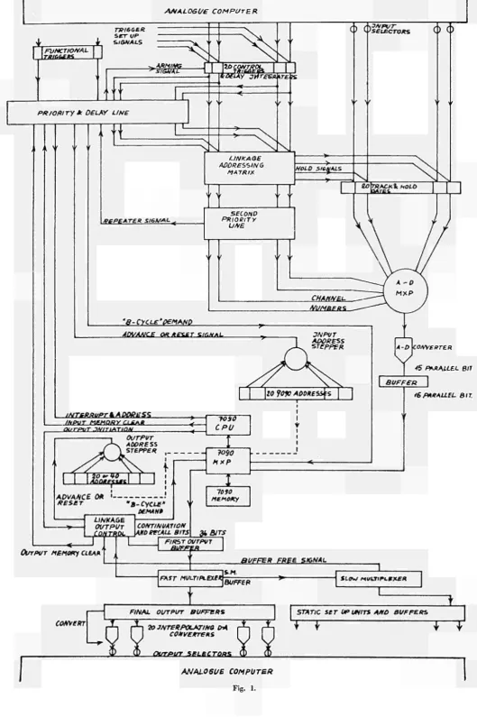
3 — DESCRIPTION OF THE LINKAGE SYSTEM PROJECTED
Flexibility is maintained throughout b y the principle t h a t each stage of data transfer should be proceed a t its own speed and call into action the next stage when its own p a r t is complete.
Thus the Α-D conversion will take place when the analogue input has changed suffi ciently to render it necessary. Thereupon, t h e conversion being complete, the digital computer will be called into action, and will itself call the D-Α conversion into operation when the pro cessing is complete.
3.1 — The analogue to digital control
Referring to the diagram, the system will be traced through this operating loop. The analogue variables are patched to a « Track and Hold Gate » and may also be connected to a « Control Trigger », which has previously been set up by the digital machine. If one of these analogue signals touches either of its limits the Control Trigger will fire, signalling both the « Linkage Addressing Matrix » (LAM) and the « Priority Delay Line » (PDL). The LAM is a matrix up to 20 X 20 in size, set up by programme before the problem is run, which relates each incoming signal to a group of from 1 to 20 outputs.
The Trigger signal thus arrives at a group of Track and Hold Gates which freeze the appropriate channels. Let us note that the number of control triggers could be 20 but in general a smaller number will suffice.
The PDL has a cycle depending on the time for multiplexing and converting one signal, and at the beginning of each cycle selects the signal of highest priority according to the nume rical order of the triggers. A signal once selected retains top priority as long as the « repeater signal » lasts (*).
When a channel signal is passed out of the PDL, it goes through the same path in the LAM as the corresponding trigger signal but because of its different form affects only the « Second Priority Line » (SPL) and not the Track and Hold Gates. When the SPL receives a single channel signal it is transmitted in this channel to the AD Multiplexer which the routes the same channel to the Α-D Converter. If two or more channels arrive simultaneously then only the first will be passed and will then be inhibited at the next passage. The « Repeater » signal will then be turned on and will cause the PDL to repeat the same channel until there is only one signal left. At this stage all inhibiters are cancelled and the next group can be accepted. Thus the PDL determines the priority of the group and the SPL priority within a group.
Data passed to the converter will be immediately converted and passed in serial form into the Α-D buffer. The address to which it is to be sent in 7090 memory is taken from a fixed table of up to 20 addresses, each of 15 bits.
These addresses have no significance for the linkage programme, and thus must not be programme set. It might be possible to retain a certain group of addresses in absolutely per manent form, but this is undesirable from the point of view of production planning since the linkage programme must be compatible with the largest possible range of digital programmes which may thus be run simultaneously.
Accordingly it is proposed to set the first 10 digits of the address group by a set of manual switches and to have the last five digits permanently wired to give the numbers from 0 to 19. When the PDL has passed a sufficient part of its cycle to permit the Α-D buffer to be filled it sends a « Β cycle » demand to the multiplexer of the 7090 which will be accepted (and cancelled) when the multiplexer is ready (about 1 microsecond) causing the multiplexer to interrogate the selected address and the data register and to store the data in the appropriate memory position.
Until the « Β cycle » answers, the PDL passes no more conversion signals. Whenever a « Repeater signal » is received a signal is passed at the end of the cycle to the Input Address Stepper (IAS) thus causing the data of one group to be stored in successive 7090 locations. If there is no repeater signal the IAS is reset and an « Interrupt » signal sent to the Central Processing Unit (CPU) of the 7090. This Interrupt is a continuous signal which remains until
(*) The PDL cycle ceases if no triggers are on and recommences immediately at the next signal.
the operation in progress is complete (a few microseconds). When it is accepted control is passed to the instruction indicated by the interrupt address which is simultaneously transferred to the Interrupt Address Buffer enabling immediate entry into the appropriate processing programming. There are two interlocks here which can stop the PDL, the first on the non-acceptance of the « Interrupt » and the second on the non-appearance of the « Input Memory Clear » (IMC) signal furnished by the programme as soon as the data from the input memories has been transferred.
There remain a few additional features on the Α-D side.
The first is the existence of a group of about 10 « Functional Control Triggers » which can generate Interrupt signals for programmes requiring no input from the analogue machine. These Triggers will be required for such functions as plotting of digital data. Secondly it is desirable to have at each of the 20 inputs a multiposition mechanical switch set or stepped by programme enabling the automatic selection of variables for conversion in static functioning. One could take 8 or 10 positions per channel according to the type of switch proposed.
Thirdly for functions of the transport delay type an additional integrater is required before the control voltage can be fed to the control triggers, since the rate of transport is the function appearing as a problem variable. This integrator will feed the control trigger directly and for this application the control trigger limits will be symmetric and pre-set. The transport rate must be made available with both signs and the input to the integrater will be switched whenever the control trigger fires.
Fourthly for certain functions the control of an accurate clock is necessary, e. g. in ite rative calculations. It is proposed to incorporate the clock directly into the PDL by-passing the triggers.
3.2 — The Digital to Analogue Control
When the 7090 has completed its processing it stocks the data to be output in a set of consecutive locations determined by manual setting up as in the case of the input. These will be selected in rotation by the Output Address Stepper, which functions in almost the same manner as the « IAS ». This implies that if overwriting is to be avoided the Output Memory Clear signal must be sent to the PDL before a new Interrupt can be admitted and thus that the time required by the output device to clear these memories must be added to the digital processing time in calculating the effective data rate. This can be avoided if a double set of output stores be used. Each digital programme must then appeal to a common subroutine and the OAS must be a circular device with 2 reset points. This will not be necessary if the output can be made fast enough, but present estimations are that the output time will be much too long to permit the simpler system.
The actual form of the output words will not be known until the detailed design of the D-Α Multiplexer is undertaken since these two items are interdependent, however the overall process is clear. At the end of the processing programme a signal of the same type as that used for calling the 7090 channels into operation is sent from the CPU to the Linkage Output Con trol (LOC). The 7090 will pass to its next job immediately after this signal is sent and if the LOC is not ready it remembers the signal and obeys it as soon as it is free. This system keeps free the most expensive unit for the maximum time. The LOC then sends a « B-cycle » demand to the 7090 Multiplexer which when ready permits the passage of information from the address shown on the OAS to the output buffer. In the output buffer it is examined for the presence of the « continuation bit » signifying that the transmission of a group of outputs is not yet completed. If the continuation bit is present the LOC will send another B-cycle as soon as it is free and will also cause the OAS to step. If there is no bit the OAS will advance to reset
position. Information in the first output buffer will be immediately passed to the DΑ Fast Multiplexer which will route it to the appropriate converter buffer or to the Slow Multiplexer buffer. The address is to be transferred as part of the data. As soon as the data is established in the appropriate buffer the LOC is released, probably by a time delay in the case of data which does not pass through the Slow Multiplexer, but otherwise by a signal. Data reaching the DΑ converter buffers will be converted to analogue form by the interpolating converters (see next section) the « Convert » signal being contained in the data transmitted by the Fast Multiplexer. The Slow Multiplexer will be used to fulfill all the static set up functions of the linkage and in most cases the units in question will in fact act as buffers.
These static linkage units will include
— the Linkage Addressing Matrix and DΑ converter modes, — Linkage input and output selectors,
— the ADIOS system, data and controls,
— the Analogue machine modes and other controls for several machines, — a group of digital potentiometers (relays switching in standard résisters), — the eventual automatic patching system,
— a group of relays for logical control of the analogue consoles (not with automatic patching) — dataplotter controls.
In every case the unit in question will signal the LOC when the data has been read. This will enable the 7090 to pass set up information in batches which will be interpreted at the rhythm of the receiving device. To call the 7090 at the end of an information group a « Recall bit » must be provided which causes the LOC to fire a Functional Trigger.
The control interlocks on the DΑ side are the Output Memory Clear, sent from the LOC and the clearing of the « Bcycle » and also the final buffer clear signals. In addition to this both ΑD and DΑ sides should interlock with the hold of the analogue machine for dynamic functioning though not for transfers to the static set up buffers. For completeness the same type of programme controlled selector could be used at DΑ output as at ΑD input.
3.3 —■ Interpolating D-Α converters
These devices function according to the relation Y = Y l + W l (X — XI)
where X I , Y l is a point of the line of which the segment chosen represents the curve in a given region and W l is its slope at that point. Note that X I , Y l is not necessarily a point of the curve. The region of validity must then be defined by two limits, in general X2, X3 (See figure 2). Note first that the generality of this representation, which might seem excessive at first glance, can be used to facilitate the construction in such a way as to render the total assembly more simple. The layout of the generalised converter is shown in figure 3. Here the point of vital importance is that only the Y l must be converted with the full number of bits for maximum accuracy, since the W l (XXl) term can be maintained as a small correction term, and the accuracy requirements on the limits are notably less severe than on Y l .
It is for this reason that the above formula is not to be simplified as Y = Y l — W l χ X I + W l χ X
AMALO SUE COMPUTER
r/tvAL OUTPUT βι/ΡϊεΑς
X2 Χ3
"Yl 'fWf ν Χ · ί V X 2 "Χ3
ffßlTS 40 BITS MO BITS 40 BITS 40 BITS
V
ν
RÉF.
MS|
Tö CONTROL·
TRIGGERS
OUTPUT ·
AMPLIFIER \
ANALOGUE.
COMPUTE*
AHPUF/Ei
ΙΛ
X
( y 2 - y * )
ΪΟΝΡυτΒΡ
variable replaces the reference. Since the solid state elements are highly non-linear this is not likely to be acceptable in the general case, at any rate according to our experiment with diode gates in Ispra, although we would be happy to have news to the contrary. On the other hand the same experiment suggested that if the range of X — XI is limited to one sign and excludes the region around zero the required accuracy could be obtained. It is for this reason that the notion of making X I equal to X2 is to be rejected. Next the idea of using only a limited set of D-Α converters with a multiplexing to a set of memories at the analogue side. Failing con trary experience the problem of setting up analogue memories sufficiently rapidly seems diffi cult to solve since the converters must supply the final multiplexer at least 10 KC/S. Thus the solution of one 15-bit and four 10-bit D-Α converters per channel is the one preferred here. A useful point to note is that for functioning in the time delay mode of operation calculation can be saved by taking the (X — XI) term direct from the delay integrater. The interpolation can be expressed in this case by the equation
Y = Y l + K (Y2 — Yl) + (T — K) (Y2 — Yl)
where Τ is the output of the delay integrater and Κ is a constant. The connection for this case is shown in figure 4 and indicates that one converter is still available to shift the origin of the multiplicative term. To note also is the provision of a range of scale factors (binary powers) for the Wl term.
4 — CONCLUSIONS
This report is intended to define the principles of the Euratom linkage and to try to indicate a path towards its' realisation. It is felt that while the needs of Euratom may seem novel, they are nonetheless common to all computation facilities above a certain minimum size. In addition it is considered that only by the type of organisation described can a satis factory general purpose linkage system be constructed. The case of handling functions of several variables by this method is notable, but the very great expansion of logical possibilities leading to rapid iteration programmes, automated optimisation, and digital overseeing and processing of the analogue results, render this linkage totally different from its predecessors in the scope of its possibilities. In short it is a step towards the integration of the two types of computer to form a genuine hybrid, rather than a slender coupling. We are, of course, still prepared to debate this view in the context of utilisation of the final product, but we would prefer to sacri fice the number of channels proposed rather than the overall principles. In any case the num ber of channels is very hard to define without operational experience but in principle it is highly desirable that the final plan should leave room for easy expansion, particularly of the logic units.