THREE PHASE INVERTER DEVELOPMENT USING COMMON MODE
VOLTAGE PULSE WIDTH MODULATION (PWM) METHOD
HASMIZAR BINTI ABD HALIM
A project report submitted in partial
fulfillment of the requirement for the award of the
Degree of Master of Electrical Engineering
Faculty of Electrical and Electronic Engineering
Universiti Tun Hussein Onn Malaysia
ABSTRACT
This master report presents a simulation voltage source control system for three
phase inverter focusing on reducing the common mode voltage using diode clamped
circuit. The model was implemented using MATLAB-Simulink with the
SimPowerSystems Block set and also M-file. The twelve Insulated Gate Bipolar
Transistor (IGBTs) was use as a switching device. In the three phase inverter circuit,
an Alternating Current (AC) output is synthesized from a Direct Current (DC) input
by closing and opening the switches in correct sequence or switching system. The
ABSTRAK
Laporan ini mengenai simulasi sistem kawalan voltan bekalan untuk penyongsang
tiga fasa menumpu kepada mengurangkan mod voltan biasa menggunakan model
litar diod diapit.Litar ini telah dilaksanakan menggunakan MATLAB-Simulink
dengan
SimPowerSystems
blok dan juga M-fail. Dua belas
Insulated Gate Bipolar
Transistor
(IGBTs) adalah digunakan sebagai suiz. Dalam litar penyongsang tiga
fasa, keluaran arus ulang-alik (AU) diroses dari masukan arus terus (AT) dengan
menutup dan membuka suis dalam susunan yang betul atau sistem pensuisan.
Pulse
Width Modulation
(PWM) merupakan satu program M-fail untuk mengawal ON /
OFF suis bagi IGBTs. Voltan keluaran penyongsang dengan model litar diod diapit
sebelum beban dan juga selepas beban akan dipantau, dibincangkan dan
dibandingkan dengan asas litar penyongsang tiga fasa. Litar penyongsang ini
beroperasi dalam sistem gelung terbuka di mana keluaran penyongsang dan beban
berhubung secara siri. Keberkesanan kaedah akan dibandingkan dengan asas
CONTENTS
TITLE
i
DECLARATION
ii
DEDICATION
iii
ACKNOWLEDGEMENT
iv
ABSTRACT
v
ABSTRAK
vi
CONTENTS
vii
LIST OF TABLES
ix
LIST OF FIGURES
x
LIST OF SYMBOLS AND ABBREVIATIONS
xii
LIST OF APPENDICES
xiii
CHAPTER 1
INTRODUCTION
1
1.1 Project Background
1
1.2
Problem
Statement
2
1.3
Project
Objective
3
1.4
Project
Scope
3
1.5
Thesis
Overview
3
CHAPTER 2
LITERATURE REVIEW
4
2.1 Introduction
4
2.2 Inverter
5
2.2.1
Three Phase Voltage Source Inverters
(VSIs)
6
2.3.2
Basic Operation of Three Phases PWM
12
2.3.3
Sinusoidal Pulse Width Modulation
(SPWM) Technique
14
2.4
Command Mode in PWM Method
18
2.4.1
Relationship between Common Mode
Current and Common Mode Voltage
18
2.4.2
Common Mode Voltage (CMV) in
Multilevel Inverter
19
2.5
Insulated Gate Bipolar Transistors (IGBTs)
23
2.6
MATLAB/
Simulink
24
2.6.1
Creating a model with Simulink
25
CHAPTER 3
METHODOLOGY
29
3.1
Introduction
29
3.2
Project Block Diagram
29
3.3
Project
Parameters
30
3.4
MATLAB/ Simulink Model for Basic Three
Phase Inverter
34
CHAPTER 4
RESULT AND ANALYSIS
36
4.1
Simulation using MATLAB/ Simulink for Three
Phase Inverter
36
4.2
Simulation using MATLAB/ Simulink for Three
Phase Inverter with Diode Clamped
43
CHAPTER 5
CONCLUSION AND FUTURE
RECOMMENDATION
50
5.1 Conclusion
50
5.2 Future
Recommendation
51
REFERENCES
52
LIST OF TABLES
2.1
Valid switch states for a three-phase VSI
9
LIST OF FIGURES
2.1
The ac output voltage produced by the VSI
7
2.2
Three-phase VSI topology
9
2.3
Circuit model of a single-phase inverter
10
2.4
Pulse width modulation signal (PWM)
11
2.5
Three-phase PWM inverter
12
2.6
Three-phase Single layer PWM inverter
13
2.7
The half-bridge VSI. Ideal waveforms for the SPWM
16
2.8
Fundamental ac component of the output voltage in a half-bridge
voltage source inverter with SPWM
17
2.9 Three-level
diode-clamped
inverter
21
2.10 Simulink
model
window
25
2.11
Three_phase_inverter.mdl
model window
26
2.12
Library Browser for Simulink
26
2.13
Sine
Wave
block in the model window.
27
3.1
Block Diagram of the 3-phase inverter
30
3.2
The parameters for all IGBTs
31
3.3
The parameters for all inductors
31
3.4
The parameters for all resistors
32
3.5
The parameters for all capacitors
32
3.6
The parameters for all RL load
33
3.7
The parameters for all clamping diode
33
3.8
The PWM signal generates 12 pulses
34
3.9
The three phase inverter
34
3.10
The three phase inverter with diode clamped
35
4.1
The three phase inverter simulation
36
4.4
Voltage for VAB of inverter before load
39
4.5
Voltage for VAB of inverter after load
40
4.6
Voltage common mode, Vcm for inverter
41
4.7
Load current and voltage for three phase inverter
42
4.8
The three phase inverter with diode clamped simulation
43
4.9
Combination Voltage for Van, Vbn and Vcn before load with
diode clamped inverter
44
4.10
Voltage for Van, Vbn and Vcn before load with diode clamped
inverter
45
LIST OF SYMBOLS AND ABBREVIATIONS
PWM
- Pulse Width Modulation
VSI
- Voltage Source Inverter
DC -
Direct
Current
AC -
Alternating
Current
SPWM
- Sinusoidal Pulse Width Modulation
EMI -
Electromagnetic InterferenceCM -
Common
Mode
IGBTs -
Insulated Gate Bipolar TransistorsNPC -
Neutral Point ClampedCSIs -
Current Source InvertersCPWM
- Continuous Pulse Width Modulation
SVPWM -
Space Vector Pulse Width Modulation
ASDs -
Adjustable
Speed
Drives
FACTS
- Flexible Alternating Current Transmission Systems
HVDC
- High Voltage Direct Current
CMV
- Common Mode Voltage
CMC
- Common Mode Current
NPP
- Neutral point Potential
MOSFET - Metal Oxide Field Effect Transistor
GUI -
Graphical User InterfaceR -
Resistance
L -
Inductance
C -
Capacitance
LIST OF APPENDICES
APPENDIX TITLE PAGE
CHAPTER 1
INTRODUCTION
1.1
Project Background
Today, the most of readymade inverter in the market are confidential and cover-up
regardless single or three phase. This is to ensure that the product will not be duplicated
or reproduced by the others and also to avoid the competition and rivalry. Generally
inverter is used in application such as induction motor, automobile, air conditioner and
etc.
In this era, an advance study in solid-state power electronic devices and
microprocessors can cause various Pulse Width Modulation (PWM) techniques
developed for industrial applications such as PWM-based three-phase voltage source
inverters (VSI) convert DC power to AC power with variable voltage magnitude and
variable frequency.The most widely used PWM schemes for three-phase voltage source
inverters is sinusoidal PWM (SPWM).
Nowadays, many studies have been done focusing on renewable energy as
alternative to generate the electricity. Examples of renewable energy from natural
sources are such as sunlight, rain and waves. In Malaysia, government is working to
accelerate the development of renewable energy, especially biomass.
By using the inverter, fuel consumption cost reduced and service for generator
also be reduced, so that there is no contamination of the environment will occur.
In this era of technological advancement and communication produced many
highly sophisticated equipment which uses digital control technology as well. To meet
the needs of this growing, then society must create the smart way in using technology to
distribute electric energy efficient, more economical and safer to use. This project will
help because the system use has the advantage of not needing additional hardware circuit
so the design will be simpler, easy to implement and more efficiency. In this project,
MATLAB/Simulink is used as a platform in designing the inverter. MATLAB/Simulink
simulation model is built to study the effect of the common mode voltage for inverter
circuit.
1.2 Problem
statement
Recently research has identified damage to electric machines caused by bearing currents.
These currents are created by the common mode voltage applied to the machine by the
inverter. In typical three-phase power inverter drives, there exists substantial common
mode voltage between the load neutral and earth ground. As modulation frequencies
increase and machine zero-sequence impedances decrease, the common mode voltage
causes larger common-mode currents, worsening electromagnetic interference (EMI)
problems and potentially damaging the network or the machine
.
The objectives of the project are:
i. To develop three-phase inverter using diode clamped circuit with common mode
voltage PWM method.
ii. To compare the analysis for three phase inverter with the three phase inverter diode
clamped.
1.4 Project
Scope
The scope of the project is to simulate the proposed method of three-phase inverter by
using common mode voltage with MATLAB Simulink software. To reduce the common
mode voltage diode clamped circuit will be added to three phase inverter circuit.
1.5 Thesis
Overview
Chapter 1 describes about the motivation, project background, problem statement,
project objectives, project scope and thesis overview. Chapter 2 covers the literature
review with
the detailed explanation and classification of voltage source inverter (VSI),
pulse width modulation (PWM) and common mode (CM) in PWM, Insulated Gate
Bipolar Transistors (IGBTs) and MATLAB/ Simulink.
Chapter 3 gives a detail study of methodology to build a three phase inverter
consist of introduction, project block diagram and project parameters. Chapter 4 shows
result and analysis for the phase inverter circuit.
Chapter 5 discusses the conclusion of advantages of the method had been
implemented into the project. This chapter also gives the recommendation about the
future development of the project.
CHAPTER 2
LITERATURE REVIEW
2.1
Introduction
Most modern power inverters produce either modified square (or modified sine) waves,
or pure sine (or true sine) waves. Modified square wave inverters don't provide the
smooth peaks and valleys that AC power from a home's electrical outlet does, but it can
deliver power that is consistent and efficient enough to run most devices. This type of
inverter is relatively inexpensive, and probably the most popular type.
Pure sine wave inverters are the most expensive, but they also deliver the
smoothest and most even wave output. Any device will run on a pure sine wave, but
some sensitive equipment, like certain medical equipment and variable speed or
rechargeable tools, requires this type of inverter to operate correctly. Radios, for
example, work better with pure sine wave inverters because the modified square wave
inverter's less smooth waves disrupt the radio's reception, causing static and other noise.
can be used for pipeline pumps in the petrochemical industry, as fans in the cement
industry, pumps in water pumping stations, traction applications in transportation
industry, steel rolling mills in the metals industry, grid integration of renewable energy
sources, for reactive power compensation and other applications.
Multilevel inverter systems are generally classified as diode-clamping inverters,
cascade inverters, and flying-capacitor inverters. Among multilevel inverters, the
three-level diode clamped inverter, which is called the neutral point clamped (NPC) inverter is
commonly used in the design. (R. Chibani et. al., 2011)
2.2 Inverter
The dc-ac converter, also known as the inverter, converts dc power to ac power at
desired output voltage and frequency. The dc power input to the inverter is obtained
from an existing power supply network or from a rotating alternator through a rectifier
or a battery, fuel cell, photovoltaic array or magneto hydrodynamic generator. The filter
capacitor across the input terminals of the inverter provides a constant dc link voltage.
The inverter therefore is an adjustable-frequency voltage source. The
configuration of ac to dc converter and dc to ac inverter is called a dc-link converter.
Inverters is, referring to the type of the supply source and topology relationship of the
power circuit, can be classified as voltage source inverters (VSIs) and current source
inverters (CSIs). In this project only the voltage source inverter will be discuss.
Modified sine wave inverters deliver power that is consistent and efficient
enough to run most devices fine. Some sensitive equipment requires a sine wave signal,
like certain medical equipment and variable speed or rechargeable tools. Modified sine
wave signal or quasi-sine wave inverters were the second generation of power inverter.
These popular types of inverters represent a compromise between the low harmonics (a
measure of waveform quality) of a true sine wave inverter and the higher cost and lower
efficiency of a true sine wave inverter.
Modified sine wave inverters approximate a sine wave and have low enough
harmonics that they do not cause problems with household equipment. They run stereos,
induction motors (including capacitor start), universal motors, computers, microwave,
TVs and more quite well. The main disadvantage of a modified sine wave inverter is that
the peak voltage varies with the battery voltage. Inexpensive electronic devices with no
regulation of their power supply may behave erratically when the direct current voltage
fluctuates.
True sine wave inverters represent the latest inverter technology. The waveform
produced by these inverters is the same as or better than the power delivered by the
utility. Harmonics are virtually eliminated and all appliances operate properly with this
type of inverter. They are, however, significantly more expensive than their modified
sine wave. (Alias I, 2007)
2.2.1 Three Phase Voltage Source Inverters (VSIs)
switches in order to generate the required high quality output voltages. However, there is
a large variety of PWM methods that exhibit unique performance characteristics and the
choice and utilization of a specific PWM method among many is not a simple task. The
tremendous amount of the literature published on PWM mostly involves the standard
Continuous PWM (CPWM) methods such as the Sine PWM (SPWM) and Space Vector
PWM (SVPWM).
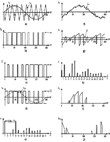
(a)
(b)
[image:17.595.152.481.279.665.2](c)
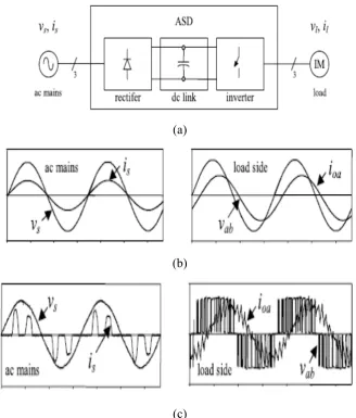
The ac output voltage produced by the VSI of a standard Adjustable Speed
Drives (ASDs) can be seen in Figure 2.1. Although this waveform is not sinusoidal as
expected (Figure 1(b), its fundamental component behaves as such. This behaviour
should be ensured by a modulating technique that controls the amount of time and the
sequence used to switch the power valves on and off.
Single-phase VSIs cover low-range power applications and three-phase VSIs
cover the medium- to high-power applications. The main purpose of these topologies is
to provide a three-phase voltage source, where the amplitude, phase, and frequency of
the voltages should always be controllable. Although most of the applications require
sinusoidal voltage waveforms (e.g., ASDs, uninterruptible power supplies and flexible
ac transmission systems), arbitrary voltages are also required in some emerging
applications (e.g., active filters, voltage compensators).
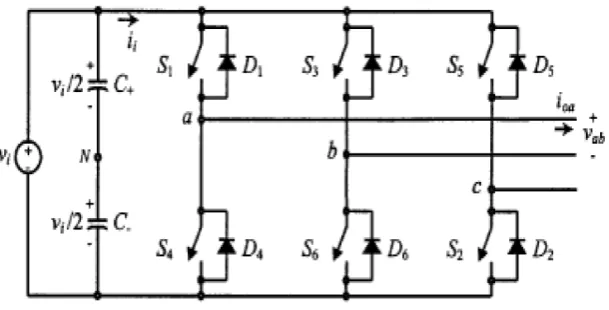
The standard three-phase VSI topology is shown in Figure 2.2 and the eight valid
switch states are given in Table 1. As in single-phase VSIs, the switches of any leg of
the inverter (S1 and S4, S3 and S6, or S5 and S2) cannot be switched on simultaneously
because this would result in a short circuit across the dc link voltage supply. Similarly,
in order to avoid undefined states in the VSI, and thus undefined ac output line voltages,
the switches of any leg of the inverter cannot be switched off simultaneously as this will
result in voltages that will depend upon the respective line current polarity.
[image:19.595.169.474.120.275.2]
(20)Figure 2.2: Three-phase VSI topology.
Table 2.1: Valid switch states for a three-phase VSI
State State Vab Vb Va Space Vector
1, 2 & 6 are ON 4, 5 and 3 are OFF 1 V 0 -V V1 = 1 + j0.5
2, 3 & 1 are ON 5, 6 and 4 are OFF 2 0 V -V V2 = j1.155
3, 4 & 2 are ON 6, 1 and 5 are OFF 3 -V V 0 V3 = -1 + j0.5
4, 5 & 3 are ON 1, 2 and 6 are OFF 4 -V 0 V V4 = - 1 - j0.5
5, 6 & 4 are ON 2, 3 and 1 are OFF 5 0 -V V V5 = - j1.155
6, 1 & 5 are ON 3, 4 and 2 are OFF 6 V -V 0 V6 = 1 - j0.5
1, 3 & 5 are ON 4, 6 and 2 are OFF 7 0 0 0 V7 = 0
4, 6 & 2 are ON 1, 3 and 5 are OFF 8 0 0 0 V8 = 0
2.3 Pulse
Width
Modulation
(PWM)
[image:19.595.116.527.368.537.2]
Many PWM strategies, control schemes, and realization techniques have been
developed nowadays. PWM strategy plays an important role in the minimization of
harmonics and switching losses in converters, especially in three-phase applications. The
first modulation techniques were developed in the mid-1960s by Kirnnich, Heinrick, and
Bowes. The research in PWM schemes has intensified in the last few decades. The main
aim of any modulation technique is to obtain a variable output with a maximum
fundamental component and minimum harmonics. (K.V. Kumar et. al., 2010)
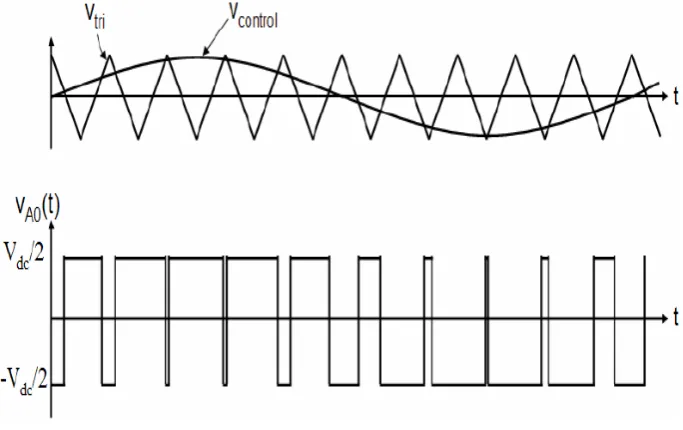
2.3.1 Basic Operation of Single Phase PWM
Figure 2.3 shows circuit model of a single-phase inverter with a center-taped grounded
DC bus. Figure 2.4 illustrates principle of pulse width modulation. (Jin-Woo. J, 2005).
As depicted in Figure 2.4 the inverter output voltage is determined in the following:
[image:20.595.136.511.477.623.2]
When Vcontrol > Vtri, VA0 = Vdc/2
When Vcontrol < Vtri, VA0 = −Vdc/2
[image:21.595.123.465.125.340.2]
(22)Figure 2.4:
Pulse width modulation signal (PWM)
Also, the inverter output voltage has the following features:
PWM frequency is the same as the frequency of Vtri
Amplitude is controlled by the peak value of Vcontrol
Fundamental frequency is controlled by the frequency of Vcontrol
Modulation index (m) is defined as:
2.3.2 Basic Operation of Three Phases PWM
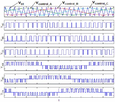
[image:22.595.124.517.274.560.2]Figure 2.5 shows circuit model of three-phase PWM inverter and Figure 2.6 shows
waveforms of carrier wave signal (Vtri) and control signal (Vcontrol), inverter output
line to neutral voltage (VA0,VB0, VC0), inverter output line to line voltages (VAB,
VBC, VCA), respectively. (Jin-Woo. J, 2005)
[image:23.595.133.504.117.445.2]
(24)Figure 2.6: Three-phase Single layer PWM inverter
As described in figure 2.6, the frequency of Vtri and Vcontrol is:
Frequency of Vtri = fs
Frequency of Vcontrol = f1
where, fs = PWM frequency and f1 = Fundamental frequency.
The inverter output voltages are determined as follows:
When Vcontrol > Vtri, VA0 = Vdc/2
When Vcontrol < Vtri, VA0 = −Vdc/2
2.3.3 Sinusoidal Pulse Width Modulation (SPWM) Technique
The ac output voltage vo = vaN follow a given waveform (e.g., sinusoidal) on a
continuous basis by properly switching the power valves. The SPWM technique fulfils
such a requirement as it defines the on and off states of the switches for one leg of a VSI
by comparing a modulating signal vc
(desired ac output voltage) and a triangular
waveform
v
Δ
(carrier signal). In practice, when vc
>
v
Δ
the switch S+ is on and the
switch S- is off; similarly, when vc < v
Δ
the switch S+ is off and the switch S- is on.
A special case is when the modulating signal vc
is a sinusoidal at frequency fc
and amplitude v^c, and the triangular signal v
Δ
is at frequency f
Δ
and amplitude v^
Δ
.
This is the sinusoidal PWM (SPWM) scheme. In this case, the modulation index ma
(also known as the amplitude-modulation ratio) is defined as
ma = v^c / v^
Δ
and the normalized carrier frequency mf (also known as the frequency-modulation ratio)
is
mf = f
Δ
/ fc
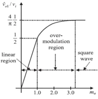
Figure 2.7(e) clearly shows that the ac output voltage vo = vaN is basically a sinusoidal
waveform plus harmonics, which features:
(a) the amplitude of the fundamental component of the ac output voltage v^01 satisfying
the following expression:
voltage appear at normalized frequencies fh
centered around mf
and its multiples,
specifically,
h = lm
f k
where k = 2, 4, 6….for l =1, 3, 5….. and k =1, 3, 5 ….for l =2, 4, 6….
(c) The amplitude of the ac output voltage harmonics is a function of the modulation
index ma and is independent of the normalized carrier frequency mf for mf > 9;
(d) The harmonics in the dc link current (due to the modulation) appear at normalized
frequencies
fp
centered around the normalized carrier frequency mf
and its multiples,
specifically,
[image:26.595.135.511.124.609.2]
(27)
Figure 2.7: The half-bridge VSI. Ideal waveforms for the SPWM (ma =0.8, mf =9):
(a) carrier and modulating signals; (b) switch S+ state; (c) switch S- state;
(d) ac output voltage; (e) ac output voltage spectrum; (f) ac output current;
(g) dc current; (h) dc current spectrum; (i) switch S+ current;
(a) For small values of mf (mf < 21), the carrier signal v
Δ
and the modulating signal vc
should be synchronized to each other (mf integer), which is required to hold the previous
features; if this is not the case, sub harmonics will be present in the ac output voltage;
(b) For large values of mf
(mf
> 21), the sub harmonics are negligible if an
asynchronous PWM technique is used, however, due to potential very low-order sub
harmonics, its use should be avoided; finally
[image:27.595.216.416.440.641.2](c) In the over modulation region (ma
> 1) some intersections between the carrier and
the modulating signal are missed, which leads to the generation of low-order harmonics
but a higher fundamental ac output voltage is obtained; unfortunately, the linearity
between
ma
and
v^01
achieved in the linear region Eq. (3) does not hold in the over
modulation region, moreover, a saturation effect can be observed in Figure 2.8. (Panda
S. et. al, 2009)
2.4
Command Mode in PWM Method
There are two types of common mode in PWM method which is Common Mode Current
(CMC) and Common Mode Voltage (CMV).
2.4.1 Relationship between Common Mode Current and Common Mode Voltage
C
ommon mode current due to modulation in power converters introduces numerous
problems in electrical systems. In aircraft, for example, inductively coupled currents
may interfere with other systems such as sensitive avionics equipment.
In industrial applications, such current can cause malfunctions of computers and
control equipment. In motor drives and electrical networks, common-mode current even
has the potential to cause physical damage or unwanted tripping of ground fault relays.
Recently, research has identified damage to electric machines caused by bearing
currents. These currents are created by the common mode voltage applied to the
machine by the inverter. In typical three-phase power inverter drives, there exists
substantial common-mode voltage between the load neutral and earth ground.
With the widespread use of the high-voltage and high power AC variable frequency
driving system and the fast development of flexible ac transmission systems (FACTS),
such as HVDC transmission, reactive power compensation, active power filter, the
multi-level inverters have caused wide concern for the researchers. However,
high-voltage high-power multi-level inverters also have accursed the severe common-mode
voltage problem.
Common-mode voltage has some disadvantages, for example, damaging the
motor winding insulation systems, causing electromagnetic interference (EMI), causing
the bearing current to fasten the bearing damage and accelerate transmission cables
ageing. To resolve the issue of the EMI, many domestic and alien scholars have reported
some effective method to suppress or cancel the common-mode voltage for the
multi-level inverter. They are mainly classified as: isolation transformer blocking method,
common-mode voltage passive filter, common-mode voltage active filter and improved
PWM control strategies.
The isolation transformer blocking method is not an economically feasible way
because the isolation transformer has the disadvantage of high cost, low efficiency, large
size and large weight. For the passive common-mode voltage filter, it will be difficult to
meet the requirements when frequency characteristics of the differential mode filter and
common mode filter are different because their equivalent circuits are the same. And the
common-mode voltage active filter, which is usually emitter follower structure, limits its
application in the high voltage field.
Multilevel inverters have been found wide spread acceptability in medium and
high voltage applications. Multilevel inverters have the advantage of producing high
voltage high power with improved power quality of the supply. It also eliminates the use
of the problematic series-parallel connections of switching devices.
Common mode voltages are generated due to the shaft voltages, circulating
leakage currents through parasitic capacitance between motor windings, rotor and frame.
So the number of current spikes and magnitude of common mode voltage is determined
by dv/dt and number of commutations. Several methods have been suggested to solve
this problem. Some methods are based on additional circuit like filters or use advanced
modulation strategies avoiding the generation of common mode voltages. But, these
methods work at higher switching frequency, thus increasing the losses.
Various multilevel inverter control techniques, using sine-triangle comparison,
for harmonic reduction have been reviewed in. But the issue of common mode voltage
control was not covered. Opportunities of harmonic reduction in cascaded multilevel
inverters were investigated in using carrier based PWM techniques. Conventional
multilevel SPWM techniques generate a significant amount of common mode voltage
which may be around the dc voltage level.
[image:31.595.155.484.123.388.2]
(32)Figure 2.9: Three-level diode-clamped inverter
Figure 2.9 is the circuit for three-phase three-level diode-clamped inverter.
Where, P is the positive point of dc bus, N is the negative point and O is the neutral
point. Each phase of the three-level inverter (taking phase-A as an example) consists of
two dc voltage dividing capacitor C1 = C2, four main switches (Sa1- Sa4), four
anti-parallel diodes (Da1-Da4) and two clamped diodes (VDa1-VDa2).
According to the definition of common-mode voltage in converter, we can know
Vcom is the common-mode voltage of converter. The expression of the Vcom is shown
as follows:
Where VAO, VBO, VCO is the phase-to-ground voltage.
Introducing the switching functions of the converter (SA, SB, SC), there are three
different switching states for each phase leg and three different output voltage levels
with respect to the neutral point for each phase. Taking one phase as an example, the
operation principles are as follows:
(a) When the switches Sa1 and Sa2 are turned on and Sa3 and Sa4 are turned off at the
same time. Assuming the load current flowing from the inverter to the load is
positive, otherwise the load current is negative. If the load current is in positive, the
current flows through Sa1 and Sa2, the phase voltage VAO is equal to Edc/2. If the
load current is negative, the current flows through VD11 and VD12 and charges the
capacitor C1, VAO is also equal to Edc/2. It is defined the switching state SA=1 at
this condition.
the load current is positive, the current flows through the main switches Sa3 and
Sa4,
VAO is equal to - Edc/2. If the load current is negative, the current flows
through the freewheeling diode which is paralleled with the main switches Sa3 and
Sa4 and charges the capacitor C2, VAO is also equal to - Edc/2. At this time SA
=-1.
So the common-mode voltage of inverter based on switching function can be expressed
as:
The common-mode voltage of inverter is only dependent on the switching state (SA, SB,
and SC). The values of Vcom have ±Edc/3, ±Edc/6, and 0. (Yonggao Z., et. al., 2012)
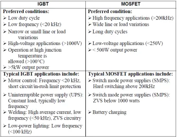
2.5
Insulated Gate Bipolar Transistors (IGBTs)
Insulated Gate Bipolar Transistorc (IGBTs) combines features from both the
FET and the BJT. Table 2.2 Show the differences between IGBTs and MOSFETs.
IGBTs are most useful in high-voltage and high-current switching applications (can
handle high collector-to-emitter voltages exceeding 200V. The basic operations of the
IGBTS are:
The input element is MOSFET and the output element is BJT
The IGBT is controlled by the gate voltage
[image:34.595.150.520.165.448.2]
(35)
Table 2.2: Differential between IGBT and MOSFET (Alias I, 2007)
2.6 MATLAB/
Simulink
REFERENCES
R. Chibani, E.M. Berkouk and M.S. Boucherit, “Study of a new DC voltage equalising
circuit for Five-Level Neutral Point Clamped-Voltage Source Inverter ”, J.
Electrical Systems 7-2 (2011): 131-148
Alias A., “Modelling and Simulation of Single Phase Inverter with PWM using
MATLAB/ Simulink”, Faculty of Electrical and Electronics Engineering,
University Malaysia Pahang, Malaysia, 2009
Panda S., Mishr A., Srinivas A B., “Control of Voltage Source Inverters using
PWM/SVPWM for Adjustable Speed Drive Applications”, Department of Electrical
Engineering, National Institute Of Technology Rourkela, Rourkela - 769008 , May
2009
K.V. Kumar, P.A. Michael, J.P. John and S.S. Kumar, “Simulation and Comparison of
SPWM and SVPWM control for Three Phase Inverter,” Asian Research Publishing
Network, Vol. 5, No. 7, pp. 61-74, July 2010.
J.Y. Lee, and Y.Y. Sun, “A New SPWM Inverter with Minimum Filter Requirement”
International Journal of Electronics, Vol. 64, No. 5, pp. 815-826, 1988.
H. Quan, Z.Gang, C. Jie, Z. Wu, and Z. Liu, “Study of A Novel Over-modulation
Technique Based on Space-Vector PWM,” IEEE Computer Distributed Control
and Intelligent Environmental Monitoring (CDCIEM), pp. 295-298, 2011.
Yonggao Z., Yanli G., lizhong L., “Study on a Common-mode Voltage Suppression
Method with High Performance for the Three-level Diode-clamped Inverter”,IEEE
2012