.~
HEWLETT
f!J
PACKARD,
COMPUTER IVIAINTENANCE COURSE
HEWLETT- PACKARD
COMPUTER MAINTENANCE COURSE
VOLUME X
STUDENTS MANUAL
EXTENDED ARITHMETIC UNIT
(HP STOCK NO. 5950-8711)
-NOTICE-The information contained in this manual is for training
purposes only. Consult the Hewlett-Packard documentation
supplied with the computer for current information
con-cerning the specific computer system furnished.
The information contained in this publication may not be
re-produced in any form without the expressed consent of the
Hewlett-Packard Company.
COPYRIGHT HEWLETT-PACKARD COMPANY 1969
11000 Wolfe Road, Cupertino, California 95014 Area Code 408257-7000 TWX 910-338-0221
Students Manual Volume X
Extended Arithmetic Unit
CONTENTS
FOREWORD
SECTION I GENERAL INFORMATION
1-l. INTRODUCTION
1-2. General Description
1-5. Installation
1-8. OPERATION
1-9. General
1-11. The EA U Instruction Set
SECTION II PROGRAMMING
2-l. INTRODUCTION
2-2. General
2-4. PROORAMMING
2-5. Multiplic ation
2-7. Division
2-10. Double Loading
2-13. Double Storing
2-16. Shift Rotate Instructions
SECTION III THEORY OF OPERATION
3-l. INTRODUCTION
3-2. General
3-4. Timing Board
3-6. Logic Board
3-8. Signal Mnemonics
3-10. THEORY OF OPERATION
3-11. Orientation
3-13. Rotate Right Logic
3-15. Rotate Left Logic
3-18. Arithmetic Shift Right Logic
3-20. Arithmetic Shift Left Logic
Students Manual Volume X
Extended Arithmetic Unit
3-22. 3-24. 3-26. 3-28. 3-30. 3-38.
Figure No.
1-1. 2-1. 3-l. 3-2. 3-3. 3-4. 3-5. 3-6. 3-7. 3 -8. 3-9. 3-10. 3-11. 3-12. 3-13.
CONTENTS (Cont'd)
Logical Shift Right Logic
Logical Shift Left Logi~
Double Load Logic Double Store Logic Multiply Logic Divide Logic
ILLUSTRATIONS
Title
Extended Arithmetic Unit Machine Coding
Format of Two- Word Dividend
Rotate Right Instruction
Rotate Left Instruction
Arithmetic Shift Right Instruction
Arithmetic Shift Left Instruction
Logical Shift Right Instruction
Logical Shift Left Instruction
Double Load Instruction
Double Store Instruction
Multiply Instruction
Divide Instruction (Part 1)
Divide Instruction (Part II)
EAU Timing Card Logic Diagram
EAU Logic Card Diagram
Students Manual Volume X
Extended Arithmetic Unit
THE EXTENDED ARITHMETIC UNIT COURSE
Foreword
FOREWORD
The Extended Arithmetic Unit (EAD) Course has been developed, under supervision of the Cupertino Division
Training Department, to teach service engineers and technicians the basic fundamentals of EAD operation
and servicing.
This course assumes that the student has an elementary understanding of common logic symbology and basic
electronics in general. As in any professional endeavor, however, proper and effective execution of the
best-planned program requires practice, skill and cooperation. The student is encouraged to study, review
and practice the course material until he is satisfied that he has mastered the basic rudiments of EAD
operation and servicing.
THE STUDENTS TRAINING MANUAL
The objective of this Students Training Manual is to provide the student with an easily accessible reference
manual which provides supplementary reading and study material, and complements the classroom lectures.
The material presented in this manual, in general, follows the logical format used in the classroom and
contains all the overhead visual slides that will be shown during the course.
The student is cautioned not to use this training manual as an operating or service manual. Those manuals
are supplied with the computer documentation provided with all HP computer systems. The student should
always consult the proper operating and service manual before attempting the operation, service, or repair
of any HP computer system. The information contained in this manual is for training purposes only.
SECTION INDEX
GENERAL INFORMATION
PROGRAMMING
Students Manual Volume X
Extended Arithmetic Unit
1-1. INTRODUCTION
1-2. GENERAL DESCRIPTION
Section I
General Information
SECTION I
GENERAL INFORMATION
1-3. The Extended Arithmetic Unit (EAU) option for HP computers permits Integer Multiply, Integer Divide,
Double Load, Double Store, Long Shifts and Long Rotations to be implemented with hardware rather than
using the programmed arithmetic subroutines. The hardware consists of two printed circuit cards. The
necessary software consists of punched tapes containing modified arithmetic and logical subroutines. The
EAU option allows data to be processed at up to 15 times as fast as it would be without the option.
1-4. The HP Interface Kit 12579A provides the necessary hardware and software to interface the EAU
op-tion with all HP series computers. The combinaop-tion of hardware and software furnished with this kit speeds
data processing without imposing any stringent programming requirements on the user. The EAU option may
be easily installed in the field.
1-5. INSTALLATION
1-6. The Extended Arithmetic Unit option may be field installed in HP2115A, HP2116A or HP2116B
Com-puters. However, for HP2116A Computers bearing serial prefix 747 - or lower, a qualified HP Computer
Service Engineer may be required to make the installation.
1-7. The EAU installation is made as follows:
a. Make certain that the computer POWER switch is set to the OFF position.
b. Insert the EAU Timing (02116-6196) and EAU Logic (02116-6202) printed circuit cards in the
appropriate slots of the computer main frame. The EAU Timing Card will plug into slot location 16
for the HP 2115A computer and slot 109 for the HP 2116A and HP 2116B computer. The EAU Logic
card will plug into slot location 17 for the HP 2115A, and slot location 110 for the HP 2116A and HP
2116B computers.
c. Return the computer POWER switch to the ON position to resume normal computer operation.
1-8. OPERATION
1-9. GENERAL
NOTE
No additional backplane wiring is required for the
HP 2116B or the HP 2115A computers. A small
amount of backplane wiring is required for the HP
2116A computers bearing serial prefix 747 - or
lower.
1-10. The Extended Arithmetic Unit requires no special programming. All EAU operations can be called
through the use of standard Assembler language, FORTRAN, or ALGOL. An EAU version of the Assembler
is furnished with this option. The mnemonics and corresponding machine instruction codes which identify
the basic EAU operations are listed in Figure 1-1. Four of these instructions (MPY, DIV, DLD and DST)
cause two computer words to be generated. operand address.
The first word is the instruction code, the second is a 15 -bit
Section I
Students Manual Volume X
General Information Extended Arithmetic Unit
MAC SIGNAL
DETERMINES INSTRUCTION
~,
'H 'H 'U
~
~, ~
I I
~
l l
~
l l l
INSTRUCTION
15
14 13
12
11
10 9
8
7
65 4
3
2
1
0
MPY 1 0 0 0 0 0 0 0 1 0 0 0 0 0 0 0
DIV
1 0 0 0 0 0 0 1 0 0 0 0 0 0 0 0OLD
1 0 0 0 1 0 0 0 1 0 0 0 0 0 0 0DST
1 0 0 0 1 0 0 1 0 0 0 0 0 0 0 0ASR
1 0 0 0 0 0 1 0 0 0 0 1*n
ASL
1 0 0 0 0 0 0 0 0 0 0 1*n
LSR
1 0 0 0 0 0 1 0 0 0 1 0*"
LSL
1 0 0 0 0 0 0 0 0 0 1 0*n
RRR
1 0 0 0 0 0 1 0 0 1 0 0*n
RRL
1 0 0 0 0 0 0 0 0 1 0 0*n
*n
NUMBER OF SHIFTS OR ROTATES
1 =1
SHIFT OR ROTATE
2=2
II II•
•
•
•
15=15
II II [image:10.617.53.531.68.531.2]0=16
II IIFigure 1-1. Extended Arithmetic Unit Machine Coding
1-11. THE EAU INSTRUCTION SET
1-12. The EAU instruction set is given in Figure 1-1. The instructions and mnemonics may be categorized
as follows:
1-2
a. The Multiply (MPY) instruction causes the computer to multiply the contents of the A Register
by the contents of a specified memory location, and to store the product in the B and A Registers
respectively. The 11 multiplic and 11 is located in the A Register, and the " multiplier" is located in a
specific memory location.
b. The divide (DIV) instruction causes the computer to divide the contents of the B and A Registers
(a two-word integer dividenci) by the contents of a memory location (the divisor): the quotient is then
stored in the A Register and the remainder is stored in the B Register.
c. The double load (DLD) instruction causes the computer to load the A and B Registers
Students Manual Volume X
Section I Extended Arithmetic Unit
General Information
d. The double store (DST) instruction causes the computer to store the contents of the A and B
Registers into two consecutive memory locations (m and m
+
1, respectively).e. The Arithmetic Shift Left (ASL) instruction causes the computer to arithmetically shift the
combined contents of the B and A Registers left (n) bits. The value of (n) may equal any number from
1 to 16.
1. The sign (B15) of the two-word quantity remains stationary and unchanged in value.
2. The most significant bits shifted out of the B-Register are discarded.
3. When vacated due to a left shift, the least significant bit position in the A-Register is
immediately refilled with a binary zero.
4. If the value of B14 remains the same as that of B15 (sign) throughout the shifting process,
ASL terminates with the OVERFLOW cleared. If, however, the values of B14 and B15 do not
remain the same throughout the operation, ASL terminates with OVERFLOW set.
f. The Arithmetic Shift Right (ASR) instruction causes the computer to arithmetically shift the
combined contents of the B and A Registers right (n) bits. The value of (n) may equal any number
from 1 to 16.
1. The sign (B15) of the two-word quantity remains unchanged in value.
2. The least significant bits shifted out of the A Register are discarded.
3. When vacated due to a right shift, the most significant bit position in the B Register is
immediately filled with a bit value "equal to that of the sign". In effect, the sign is extended
to the right as a result of the ASR operation.
g. The Logical Shift Left (LSL) instruction causes the computer to logically shift the combined
contents of the B and A Registers left (n) bits. The value of (n) may equal any number from 1 to 16.
1. The most significant bits shifted out of position B15 of the B Register are discarded.
2. When vacated due to a left shift, the least significant bit position in the A Register is
immediately filled with a binary zero.
h. The Logical Shift Right (LSR) instruction causes the computer to logically shift the combined
contents of the B and A Registers right (n) bits. The value of (n) may equal any number from 1 to
16.
1. The least significant bits shifted out of position AO of the A Register are discarded.
2. When vacated due to a logical right shift, B15 is immediately filled with a binary zero.
i. The Rotate Left (RRL) instruction causes the computer to rotate the combined contents of the B
and A Registers to the left (n) bits. The value of (n) may equal any number from 1 to 16.
1. No information is discarded.
2. The most significant bit (B15) rotated out of the B Register reappears as the least significant
bit (AO) in the A Register.
j. The Rotate Right (RRR) instruction causes the computer to rotate the combined contents of the B
and A Registers to the right (n) bits. The value of (n) may equal any number from 1 to 16.
1. No information is discarded.
2. The least significant bit (AO) rotated out of the A Register reappears as the most significant
bit (1315) of the B Register.
1-13. Programming procedures for the EAU instruction set are given in Section II. A functional theory of operation is given in Section III.
•
Students Manual Volume X
Extended Arithmetic Unit
Section II
Programming
SECTION II
PROGRAMMING
2-1. INTRODUCTION
2-2. GENEHAL
2-3. The Extended Arithmetic Unit requires no special programming. All EAU operations can be called
through the use of standard Assembler language, FORTRAN, or ALGOL. An EAU version of the Assembler
is furnished with this option. The mnemonics and corresponding machine instruction codes which identify
the basic EAU operations are listed in Figure 1-1. Four of these instructions (MPY, DIV, DLD, and DST)
cause two computer words to be generated. The first word is the instruction code, and the second is a 15
bit operand address. The manner in which the basic Extended Arithmetic Unit operations may be called and
examples of obtainable results are described in subsequent paragraphs of this section.
2-4. MULTIPLICATION
2-5. Calling the multiply (MPY) instruction causes the computer to multiply the contents of the A Register
by the contents of a memory location, and to store the product into registers B and A, respectively.
2-6. The following are examples of programming the multiply instruction in FORTRAN and Assembler
language:
a. FORTRAN: Multiply quantities I and J and store the result in M.
b. Assembler Language:
Label OP Code Operand
MPY m[,I]
lit
m absolute or relative address
expression
I Indirect addressing
indica-tor
lit literal value
The result is stored right-justified in the combined B and A Registers.
2-7. DIVIDE
2-8., Calling the divide (DIV) instruction causes the computer to divide the contents of Registers B and A
(a two-word integer quantity) by the contents of a memory location; the quotient is stored in the A Register
and the remainder is stored in the B Register.
2-9. Examples of programming the DIV instruction in terms of FORTRAN and Assembler language are as
follows:
a. FOHTRAN: Divide the two-word integer quantity I by the integer quantity J and store the
result in M.
M=I/J
Section II Programming
Students Manual
Volume X
Extended Arithmetic Unit
b. Assembler Language:
Label OP Code
DIV
m
lit
Operand
m[,I] lit
absolute or relative address
indirect addressing indica-tor
literal value
Initially, the two-word dividend is stored in the B and A Registers in the combined,
right-justified form shown in Figure 2-1. At the completion of the division process, the A Register
contains the quotient and the B Register contains the remainder. If an attempt is made to divide
by zero, or if a divide operation results in a quotient too large for the A Register, the OVERFLOW
bit will be set to signify that the results are invalid.
~I"--B-REGISTER ----~--A-REGISTER -~"I
15 14 13 12 11 10 9 8 210
\~ ______________________________ ~r ________________________________ ~J
y
[image:14.612.83.528.288.481.2]DIVIDEND
SIGN OF DIVIDEND
Figure 2-1. Format of Two-Word Dividend
2-10. DOUBLE LOADING
2-11. Calling the double load (DLD) instruction causes the computer to load the A and B Registers
(res-pectively) with the contents of two consecutive locations (m and m
+
1) in memory.2-12. An example of programming the DLD instruction in terms of Assembler language is as follows:
a. Assembler Language (DLD) sequence:
Label OP Code
DLD
m
lit
2-13. DOUBLE STORING
Operand
m[, I] lit
Location of first word; contents of this location are
loaded into A Register. Contents of location m + 1
are loaded into B Register
Indirect addressing indica-tor
literal value (F only)
2-14. Calling the double store (DST) instruction causes the computer to store the contents of the A and B
Students Manual Volume X
Extended Arithmetic Unit
Registers into two consecutive memory locations (m and m + 1, respectively).
Section II Programming
2-15. An example of programming the DST instruction in terms of Assembler language is as follows:
a. Assembler Language (DST) sequence:
Label OP Code
DST
m
I
2-16. SHIFT-ROTATE INSTRUCTIONS
Operand
mLI]
Location of first word; the contents of the A Register are stored in this location. Contents of the B
Register are stored in location m + 1.
Indirect addressing indicator
2-17. In EAU equipped computers, the combined contents of the B and A Registers (in that order) can be
shifted or rotated, left or right, in bytes of from 1 to 16 bits per instruction. Paragraphs 1-12e thru 1-12j
describe the shift-rotate instruction set.
2-18. Programming the shift-rotate instructions in Assembler language is direct and simple:
a. ASL (m): arithmetic shift left (m) bits
b. ASR (m): arithmetic shift right (m) bits
c. LSL (m): logic shift left (m) bits
d. LSR (m): logic shift right (m) bits
e. RRL (m): rotate left (m) bits
f. RRR (m): rotate right (m) bits
Students Manual Volume X
Extended Arithmetic Unit
3-1. INTRODUCTION
3-2. GENERAL
Section III
Theory of Opera'tion
SECTION III
THEORY OF OPERATION
3-3. Figures 3-12 and 3-13 are the logic diagrams for the two printed circuit boards that comprise the
Extended Arithmetic option. Basically, the Extended Arithmetic Timing board provides timing signals to
the Extended Arithmetic Logic board. Major functional blocks are identified by shaded areas on the logic
diagrams for ease of location of function.
3 -4. TIMING BOARD
3 -5. The EAU option is enabled by a true signal (MAC) to pin 62 of the Timing board. This signal is true
when bits 15 through 12 of the instruction word are 1-0-0-0, and bit 10 is O. The remaining bits (TRO
through TR9 and TRll) code the specific EAU instruction as indicated in Figure 1-1. The Inhibit Processor
logic disables the Instruction Register and phase circuits in the processor, permitting the Memory and
Phase Control logic to generate the necessary P123 phase signal. The Operation Decoder determines the
type of operation to be performed (Arithmetic Shift, Logical Shift, Rotate, Multiply, Divide, Right Shift or
Rotate, Double Load, Double Store), and the Operation Cycle Counter, Operation Cycle Decoder, and MP2
Gating logic determine how many memory cycles (or operations) will be used in executing the instruction.
The Shift logic provides shift function signals to the Logic board, and the Overflow logic drives the
Over-flow indicator circuits in the processor. The Operation Exit logic ends the entire operation by advancing the
P Register to the next instruction (via the Logic board), and resetting appropriate EAU circuits.
3-6. LOGIC BOARD
3 -7. The 23 functional blocks indicated by shading identify each of the functions involved in executing the
EAU instructions. The EAU timing signals from the Timing Board are shown as inputs at the left of the
figure. Basic computer timing signals are shown as inputs at the lower right. Four of the functional blocks
are outputs to the R-S-T buses of the computer (SBO, TB15, TBO, RBO). Five blocks provide special EAU
bit manipulations (Link, Carry, Sign, Overflow, Shift Overflow). Four blocks provide function signals
similar to corresponding function signals in the basic processor (Complement Function, Add Function,
Ex-clusive "Or" Function, Multiplication Add Function). Read and Store signals from the remaining ten blocks
enable data transfers to and from the Registers in the same manner as corresponding signals generated on
the Instruction Decoder Board in the basic processor.
3-8. SIGNAL MNEMONICS
3-9. Table 3-1 lists definitions of mnemonics relating to the Extended Arithmetic option. These include
signal names defined for the basic processor, as well as names unique to the EAU option. An X ( Extended
Arithmetic) or a B ( Buffered ) is used in some cases to identify a signal generated by the option, but is
otherwise similar or identical to a signal generated elsewhere in the processor.
3-10. THEORY OF OPERATION
3-11. ORIENTATION
3-12. The theory of operation will be described using flow charts to show the implementation of each EAU
Section III
Theory of Operation
Students Manual Volume X
Extended Arithmetic Unit
instruction described in Sections I and II. The following descriptions will also reference the logic diagram,3
given as Figures 3 -12 and 3 -13. The logic signals are given in Table 3-1.
TABLE 3-1. EXTENDED ARITHMETIC OPTION MNEMONICS
SIGNAL DEFINITION SIGNAL DEFINITION
ADF Add Function PlRB Plus 1 onto R Bus AS Arithmetic Shift PlSB Plus 1 onto S Bus
P123 PHI-PH2-or-PH3 signal
C16 Carry bit 16 PHI Phase 1, fetch CARX Carry flip-flop (EAU) PH5 Phase 5, optional CLF Clear Flag signal
CMFB Complement Function, Buffered RARB Read A onto R Bus CRS Control Reset signal to I/O RBO-15 R Bus bits 0-15 CTOO Counter at Operational Zero RBRB Read B onto R Bus
RF2 Run flip-flop 2 01-6 Divide operation cycles 1-6 RMSB Read M onto S Bus
05L8 D5, Loop 8 RO Rotate
DIV Divide ROT5 Rotate at T5
DL1-4 Double Load operation cycles 1-4 RPRB Read Ponto R Bus
OLD Double Load RSDS Reset, Double Store Operation DSl-4 Double Store operation cycles 1-4 RSET Reset CARX flip-flop (EAU) DST Double Store RT Right shift or rotate
RTSB Read Tonto S Bus
EOFI3 Exclusive Or Function, Buffered
EPH Enable Phase Signal SBO-15 S Bus bits 0-15 EPIIX Enable Phase flip-flop (EAU) SDD Sign of the Dividend EXIT Exit MAC operation sequence SDV Sign of the Divisor
GATE Gate flip-flop SIGN SLMB Sign of the Operand Shift Left Magnitude, Buffered I1R Inhibit Instruction Register SL14B Shift Left bit 14, Buffered I1RX IIR flip-flop (EAU) SMD Sign of the Multiplicand IOSB I/O Switch address, Buffered SMR Sign of the Multiplier ISG Inhibit Strobe Generator SQT Sign of the Quotient
LINK Li!1k flip-flop SRCS Shift/Rotate Count Started LS Left Shift SRMB Shift Right Magnitude, Buffered
STF Set Flag, decoded MAC Macro t;roup, decoded SWSA Switch Store into A MAF Multiplication Add Function SWSB Switch Store into B MD1-ti Multiply /Divide operation cycles 1-5 SWSM Switch Store into M M02G MD2, Gated SWSP Switch Store into P MPl-5 Multiply operation cycles 1-5 SWST Switch Store into T MPY Multiply
TO-7 Time Periods 0-7 OASL Overflow due to Arithmetic Shift Left TBO-15 T Bus bits 0-15
OCO-3
oce
flip-flops 0-3 TEV Time bits, Even numbered OCC Operation Cycle Counter (TO, T2, T4, T6) OVD Overflow due to Divide operations TOD Time bits, Odd numbered OVF Overflow flip-flop (Tl, T3, T5, T7) OVR Overflow Register TS Time Strobe [image:18.618.100.481.171.532.2]Students Manual Volume X
Extended Ar ithmet ic Un it
3-13. ROTATE HIGHT LOGIC
3-14. The Ilotate Right (RRR) instruction flowchart is shown in Figure 3-1.
T5
TO-3 ... CTR
0 - EPH
1 - l l R
o
-P123AO-C B - L
9
YES
P+1-P,M 1-EPH
O-IIR
[image:19.615.69.565.113.406.2]t - - - I ..
Figure 3-1. Rotate Right Instruction
Section III
Theory of Operation
The number of rotates to be performed, 3 in our example, will be applied as one true binary input to the
re-set side of the Operation Cycle Counter Flip-Flops located on the EAU Timing Board (Figure 3-12). The RRR
instruction will make bits 6, 9 and 15 true. Bit 6 will set the Right Shift or Rotate (RT) Flip-Flop. The
en-abling signal for these flip-flops is the MAC signal which is true when bit 15 ::: 1, 14
=
0, 13=
0, 12=
0, and10
=
o.
This signal enters on pin 62 and is the enabling input to the gates that will set the RO (Rotate) and RT Flip-Flops. The flip-flops will be set on T3TS of PH1 by the output of MC115A. At T5, T Register bits 0thru 3 are read into the Operation Cycle Counter. The enabling signal to the Enable Phase Flip-Flop (EPHX
FF) is false and therefore a change of phase is not permitted. Also, the signal to inhibit the I Register (IIR)
is true, preventing the I Register from losing the instruction. Since RO and RT are set, A Register bit 0 is
rotated into the Carry Flip-Flop (Figure 3 -12) via the TBO line. At T6, the contents of the B Register are
rotated right one bit position. The Carry Flip-Flop (CARX FF) contents are now rotated into B Register bit 15
and B Register bit 0 is rotated into the Link Flip-Flop. At T7: the A Register contents are rotated right one
bit position; the contents of the Link Flip-Flop are rotated into A Register bit 15; A Register bit 0 is rotated
into the Carry Flip-Flop; and the Cycle Counter contents (minus one) are shifted back into the counter. Also
at T7; the Exit Flip-Flop is looked at and, if reset, the operations that took place at T6 and T7 are repeated
until the Exit Flip-Flop is set. When the Exit Flip-Flop is set (and it is T6 or T7), the T6T7 clock cycle must
be repeCated. Then at T6T7 of the current clock cycle, the P Register is incremented and the results are
stored back into the P and M Registers. The signal (P123) to enable the phase is now made true. This is
ac-complished by the true exit signal which enters at pin 74 on the Timing board. At T7 of the clock cycle, MC83A
is enabled and the Enable Phase (EPHX) Flip-Flop is set. The signal to IIR is now false and the I Register is
permitted to reset. This ends the RRR instruction operation.
Section III
Students Manual Volume X
Theory of Operation Extended Arithmetic Unit
3-15. ROTATE LEFT LOGIC
3 -16. The Rotate Left (RRL) instruction flowchart is shown in Figure 3-2. The number of rotates to be
performed (3 in our example) will be coded in bit positions 0 thru 3. The bit positions that are true are
applied as an enabling signal to reset the Operation Cycle Counter Flip-Flops (F igure 3 -12). Bit 6 being
true will set the Rotate (RO) Flip-Flop (MC96B). Bits 15, 14, 13, 12, and 10 will enable the MAC signal.
At T5, T Register bits 0 thru 3 are read into the Operation Cycle Counter. The enable phase sign~l (EPHX)
is now made false and a true IIR signal is enabled to the Instruction Register. A false signal is also sent to
Phase 123, and B Register bit 15 is rotated left into the Carry Flip-Flop. At T6 a SLM signal ['otates the A
Register left one position and the contents of the Carry Flip-Flop are rotated left into A Register' bit O. The
A Register bit 15 is then rotated left into the Link Flip-Flop, and A Register bit 14 is rotated left into A
Reg-ister bit 15. At T7 a SLM signal rotates the B RegReg-ister left one position. The Link Flip-Flop contcnts are
then rotated into B Register bit 0 and B Hegister bit 15 is rotated into the Carry Flip-Flop. The I~ Register
bit 14 is rotated into bit 15, and a minus one is shifted into the Cycle Counter.
3 -17.
T5 T6 ( TO )(T2 )(T4) SLM A --A C -AO A15-L A14-A15
YES
T7(T1)( T3)(T5) SLM
B - B
L --+ BO B15-+C B14-B15 CTR-1 .. CTR
P+1~tM
1--.EPH
1---1.,
[image:20.617.47.535.297.554.2]O-IIR
Figure 3-2. Rotate Left Instruction
At the end of T7, if the Exit Flip-Flop is not set, the same operations that occurred at T6 and T7
will be repeated at TO of the next machine cycle. When the Exit Flip-Flop is set, and the clock is at T6 or
T7: another T6T7 clock cycle occurs. The P Register is now incremented and the result is stored back in
the P and M Registers. The Enable Phase FF is set and the I Register is not inhibited (IIR). This cnds the
RRL instruction operations.
3 -18. ARITHMETIC SHIFT RIGHT LOGIC
3 -19. The Arithmetic Shift Right (ASR) instruction flowchart is shown in Figure 3 -3. The ASR routine
begins at T5 with T Register bits 0 thru 3 applied as a reset signal to the Operation Cycle Counter on the
Timing board (Figure 3-12). A reset signal is then applied to the Enable Phase Flip-Flop. Resetting the
Students Manual Volume X
Extended Arithmetic Unit
Section II
Theory of Operation
EPHX Flip-Flop prevents the machine phase from changing. The IIR signal is then made true and a false
P123 signal is taken from pin 13 on the Timing board. At T6 a SRM signal (from pin 41 on the Timing board)
shifts the contents of the B Register right (n) places and bit 15 is shifted back into bit 15 (the sign bit). B
Register bit 0 is shifted into the Link Flip-Flop. At T7 a SRM signal shifts the contents of the A Register
right (n) placeR, and the Link Flip-Flop contents are shifted right into A15. The cycle counter contents minus
one are then stor'ed into the Operation Cycle Counter. If the Exit Flip-Flop is not set, the same operation
that occurred at '1'6 is repeated at TO, T2, T4 and the same operation that occurred at T7 is repeated at T1,
T3 and T5. The cycle will loop until the Exit Flip-Flop is set. This will end the ASR operation .
...-_T_5... T6(TO)(T2)(T4) T7(T1)(T3)(T5)
B~B ASRM~A
B15-..815 L~A1
eTR -1 .. eTnl---I~
[image:21.613.66.559.212.469.2]NO
Figure 3·3. Arithmetic Shift Right Instruction
3-20. ARITHMETIC SHIFT LEFT LOGIC
3-21. The Arithmetic Shift Left (ASL) instruction flowchart is shown in Figure 3-4. At T5 T Register
bits 0 thru 3 are applied to the Operation Cycle Counter, and a false signal is sent to the EPHX Flip-Flop.
A true IIR signal goes to the Instruction Register and a false signal goes to Phase 123. The CARX (Carry)
Flip-Flop is also cleared. At T6 a SLM signal shifts the contents of the A Register left (n) places and a
zero is forced into AO; A15 is read into the Link Flip-Flop and A14 is read into A15. At T7 a SLM signal
shifts the contents of the B Register (n) places and the Link Flip-Flop contents are shifted into BO. B
Reg-ister bit 15 remains the same, and B15 and B14 are compared. If they are the same, OVF is cleared. If
different, the OVF is set, and the Cycle Counter is "decremented". If the Exit Flip-Flop is not set the
shifting operation that occurred at T6 is repeated at TO, T2 and T4. When the Exit Flip-Flop sets the ASL
operation terminates.
3-22. LOGICAL SHIFT RIGHT LOGIC
3-23. The Logical Shift Right (LSR) instruction flowchart is shown in Figure 3-5. At T5 T Register bits 0
thru 3 are read into the Operation Cycle Counter, a false signal goes to the EPHX FF, a true IIR signal goes
to the Instruction Register, and a false P123 signal is generated. At T6 a SRM signal shifts the contents of
the B Register and BO is shifted into the Link Flip-Flop. Bit AO is then forced into B15. At T7 a SRM
sig-nal shifts the contents of the A Register (n) places and the Link Flip-Flop is shifted into A15. The Cycle
Counter is "decremented". If the Exit Flip-Flop is not set, the (T6) (SRM) and (T7) (SRM) operations are
looped at TO, T2, and T4; and T1, T3 and T5, respectively. When the Exit Flip-Flop sets the operation
Section II
Theory of Operation
:3 -6
T5 T6 (TO )(T2)(T4) T 7{ T1}(T 3)(T 5)
TO- 3.CTR
A~A
B.£!i BO--..EPH O--+- AO L--BO
A15 ... L B15~ B15
A14 .... A15 B15
+
B14o
----..C ~OVF [image:22.613.50.556.70.717.2]CTR--J.CTR
Figure 3-4. Arithmetic Shift Left Instruction
T5 T6(TO)(T2)(T4) T7(T1){T3)(T5)
----""II
TO-3+CTR
O--+EPH
1---+ IIR
O-P123
B~B
BO-L
o
---+B15A~A
Figure 3-5. Logical Shift Right Instruction
NO
NO
Students Manual Volume X
Students Manual Volume X
Extended Arithmetic Unit
3-24. LOGICi\ T J SHIFT LEFT LOGIC
Section II
Theory of Operation
3-25. The Logical Shift Left (LSL) instruction flowchart is shown in Figure 3-6. At T5 T Register bits 0
thru 3 are applied as reset inputs to the Operation Cycle Counter, and a false signal goes to the EPHX FF, a
true signal is sent to IIR, and a false signal to P123. At T6 a SLM signal shifts the contents of the A Register
(n) places and a zer'o is forced into AO; A15 is shifted into the Link Flip-Flop, and A14 is shifted into A15.
At T7 a S LM signal shifts the contents of the B Register (n) places. The Link FI ip-Flop is shifted into EO
and B14 is shifted into B15. The counter is then "decremented". If the Exit Flip-Flop is not set the (T6)
(SLM) and (T7) (SLM) operations are repeated at TO, T2 and T4; and at T1, T3 and T5, respectively. When
the Exit Flip-Flop sets the LSL operation terminates.
T5 T6 (TO)(T2)(T4) T7(T1)(T3}(T5} TO-3-CTR
A~A
8 SLM., 8 O--+EPH O~AO L ---8 01 - I I R A15-+-L 814-+815
A14 ... A15 CTR-1.c
[image:23.615.67.565.236.459.2]NO
Figure 3-6. Logical Shift Left Instruction
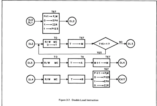
:~ -26. DOUBLE LOAD LOGIC
3 -27. The Double Load (DLD) instruction flowchart is shown in Figure 3 -7. The format for this instruction
- - -
-is bit 15, 11, and 7 true and all others false. Bits 15, 14, 13, 12, and bit 10 make the MAC signal true, and
l;>it 7 will enable MC 12 7B (on the Timing board). The output is applied to MC127C and this true output will set
the DLD Flip-Flop (MC126B). At T6T7 of DLD cycle 1 the P Register is incremented and the results are
stored back into the P and M Registers. A false signal goes to the EPHX FF, a true IIR signal to the
Instruc-tion Register, and a true signal is sent to P123. At TO of DLD cycle 2, the T Register is cleared, and a read/
write memory cycle begins. Then at T6T7 the contents of the T Register are read into the M Register. If
"indirect address ing", then a loop is made back to the beginning of DLD cycle 2 (until TB15
=
0). At TO ofDLD cycle 3, there is a read memory cycle. Then at T4 the contents of the T Register are loaded into the
A Register. At T6T7 the M Register is incremented and the results are stored back into the M Register. At
TO of DLD cycle 4, there is another read memory cycle. Now at T4 the T Register contents are loaded into
the B Register. At T6T7 the P Register is again incremented and the results are stored back in the P and M
Registers. Now there is also a false signal at P123, a true signal to the EPHX FF, and a false IIR signal to
the Instruction Hegister. When the Exit Flip-Flop sets, the DLD operation terminates.
Section III
Theory of Operation
T67
Pt1-+ P,M
o
- - + E P H ~----jN1--+IIR 1 ---.P123
Students Manual
Volume X
Extended Arithmetic Unit
~
____
~T~O~ ~____
~T~4_ T678--1_R_'_W __
M_C~H
T
-A
HM
+1-+M
l--8
T673-28. DOUBLE STORE LOGIC
P+1-..P,M 0----+ P12 1---+EPH
o
---+IIRFigure 3-7. Double Load Instruction
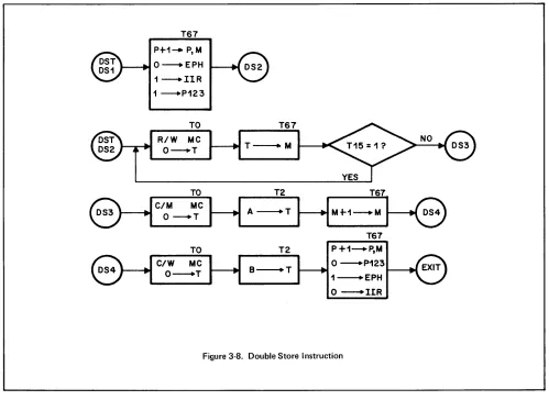
3-29. The Double Store (DST) instruction flowchart is shown in Figure 3-8. The format for this instruction
is bits 15, 11 and 8 true. All other bits are false. The MAC signal (bit 8) and bit 11 being true will set the
DST Flip-Flop (MC126A). During Double Store cycle 1 at T6T7, the P Register is incremented and the
re-sults stored back into the P and M Registers. There is now a false EPH signal, a true IIR signal, and a true
P123 signaL During Double Store cycle 2 the T Register is cleared at TO and a read memory cycle occurs.
At T6T7 the contents of the T Register are stored into the M Register and if bit 15
=
1, the loop is repeatedstarting at TO until bit 15
=
0 (indirect addressing). During Double Store cycle 3, the T Register is clearedat TO and a write memory cycle occurs. At T2 the A Register contents (n) are stored into the T Register.
At T6T7 the P Register is incremented and stored back into the P and M Registers. During Double Store
cycle 4, the T Register is cleared at TO and a write memory cycle occurs. The B Register contents are
read into the T Register at T2 and at T3 -T5 this data is stored into memory (m + 1). At T6T7 the P Hegister
is iIfcremented and the results are stored back in the P and M Registers. A false P123 signal, a true EPH
signal, and a false IIR signal are then enabled. When the EXIT FF sets the operation is terminated.
3-30. MULTIPLY LOGIC
3 -31. The Multiply (MPY) instruct ion flowchart is shown in Figure 3 -9. The MPY instruction (100200)
decoded will make bit 15 and bit 7 true. All other bits will be false. Bits 15
=
1, 14 = 0, 13 = 0, 12 c: 0and bit 10
=
0 will make the MAC (macro-group decoded) signal true. This true signal enters at pin G2 (on [image:24.615.43.548.86.425.2]Students Manual Volume X
Extended Arithmetic Un it
Section III
Theory of Operation
the EAU Timing board) and enables MC97B. The true output on pin 13 of MC97B is applied as one true input
to MC127A, MC127C, MC97A. MCll7C, MC117A, MC97C, MC107A, and MC107C. The other true bit is
bit 7 and it is applied as a true input to MC127B (via pin 83). The true output at MC97B pin 13 is also applied
as a true input to MCll7A. The other true input to MCl17A is from the TRll line. The TRll signal enters
at pin 70 and enables MC107B. The output on pin 13 is applied as a true input to MC1l7A. Gate MC117A is
enabled and its it'ue output is applied to the MPY Flip-Flop (MCl16A). This sets the MPY Flip-Flop when the
clock signal is applied via the CRS signal. The clock signal may also be supplied by a true output from MCll5A
which is enabled at (T3) (PHl) (TS). The other way to supply a clock pulse is to enable MC103B, by a Reset
Double Store operation (RSDS). With the MPY Flip-Flop set, its set side output is applied to MCl16Gl. The
other true input to enable MCl16G1 is from :vrC87A. Gate MC87A will have a true output when there is not a
Phase 5 operation (DMA), or when the Run Flip-Flop is set, The true output from MCl16G (pin 13) is applied
to MC86A, MC42A, MC17B, MC17A, MC27B, and MC27A. The true output from MC86A (pin 2) is then
ap-plied to MC54C and to MC77B. Gate MC77B is enabled because the input (pin 9) is true, pin 8 is true, pin 7
is true, and at the timing strobe of T7, pin 6 is true. The true output is applied as a clock pulse to each of the
Operation Cycle Counter Flip-Flops. The first phase of the MPY instruction is now in progress.
T67 P+1-+ P,M O--+EPH 1--+IIR 1 --+P123
T67
HMH--+M~
T67 P +1---+P,M
o
--.P1231~EPH
[image:25.612.57.556.326.690.2]o
---+IIRSection III
Theory of Operation
T2 T3
T4 P+1~P,M
O - - E A15 __ SMr.--... c: NO
3-10
T0
R/W MC
O----+-T
T67
T ---+-M t - - . . c
YES
INDIRECT
T2(T6) SRM B----+-B B0--.-L 0----..B15
T3(T7) SRM
A ----....A
L~A15
A0----+- FA
[image:26.615.51.549.63.715.2]LOOP X 16
Figure 3-9. Multiply Instruction
T67
P+1----P,M 1--+EPH
o
---IIRO~MPY
O~OVD
NO
Students Manual Volume X
Students Manual Volume X
Extended Arithmetic Unit
Section III
Theory of Operation
3 -32. The multiplicand which is stored in the A Register is now read into the B-Register. At the same time,
A Register bit 15 is read into the SMD/SDD Flip-Flop (MC43A is located on the EAU Logic board). If this bit
is true (T bus enters at pin number 80) it will set the SMD/SDD Flip-Flop indicating that the multiplicand is
of negative value. When the sign of the multiplicand is negative, the computer will complement the contents
of the B Register, add one to it, and store the results back in the B Register. If the sign of the multiplicand
is positive (bit 15
=
0) the SMD/SDD Flip-Flop is not set and the complement-increment operation of the BRegister does not take place. At T6T7 the P Register is incremented, and the results are stored back into
the P and M Registers. The Enable Phase signal (EPH) is made false and therefore, the computer cannot
enable the phase. The signal to enable the P123 signal is made true, however, so a memory read and write
cycle may be enabled. The signal to inhibit the I Register (IIR) is made true so the contents of the I Register
do not change. Now the computer is ready to proceed to Memory Cycle 2 (M2).
3 -33. Memory Cycle 2 (M2) begins with resetting the T Register Flip-Flops, and the read memory cycle
reads the contents of a specific memory location into the T Register. Now the T Register contains the address
of the multiplier. During T6T7 the T Register contents are read into the M Register. Now the M Register
contains the address of the multiplier. Also, bit 15 is looked at to see if it is true or false. This will
de-termine if the address is the final address of the multiplier or if another memory cycle is needed to get the
final address (indirect). This loop is repeated until bit 15 is a O. When bit 15 is
a
0 the computer goes intomemory cycle 3 (M3).
3 -:~ 4. Memory cycle 3 (M3) begins with resetting the T Register Flip-Flops, and then the read memory
cycle reads from'Ylemory the multiplier. Next the multiplicant, which is in the B Register, is read into the
A Hegister. Bit BO is read (via the T-bus) into the MAF Flip-Flop. The T-bus bit 0 (TBO) enters at pin 79
Oil the EAU Logic Board, and this signal is applied as an input to the MAF Flip-Flop (MC73A). The
multi-plier, which is in the T Register, is now read into the B Register. The sign of the multiplier is looked at by
reading T-bus 15 (TB15) into the sign of the Multiplier Flip-Flop. This TB15 signal enters at pin 80 on the
EI\U Logic board and is applied as an input to the SMR/SDV Flip-Flop (MC43B). The sign of the multiplier
is tested and if the sign is positive (bit 15"= 0) the B Register contents are read into the M Register, and the
Phase 123 signal is made false. If the sign of the multiplier is negative (bit 15
=
1), the contents of the BH(~gister are complemented, read into the M Register, and then the Phase 123 signal is inhibited. The Phase
12:~ signal is generated on the Timing board by MC12B, located in the Memory and Phase Control block. If
the sign of the multiplier is positive, after disabling the P123 signal, the B Register is cleared at T6 and
again at T7 the P123 is disabled. Now the computer is ready to go to Memory cycle 4 (M4).
3 -35. Memory cycle 4 (M4) begins with testing the MAF Flip-Flop at TOT!. If the MAF Flip-Flop (MC73A
located in the Multiplication Add Function block on the Logic board) is set, the contents of the B Register are
added to the contents of the M Register, and the result is stored back into the B Register. If the MAF
Flip-Flop is not set the previous operation does not take place, and at T2 a Shift Right Magnitude (SRM) signal
(which comes from pin 41 on the EAU Timing board) will shift the B Register contents right one position.
Bit 0 will be shifted into the Link Flip-Flop (MC112B). This is accomplished by R Bus (RBO) which enters
on pin 43 of the Logic board and enables MC123D. Bit AO is then forced into bit 15. At T3, a Shift Right
Magnitude signal (SRM) shifts the A Register right one position. The Link Flip-Flop is shifted into the bit 15
position of the A Register. The
A
Register bit 0 is shifted into the MAF Flop. At T4T5 the MAFFlip-Flop is again tested and, if set, the Band M Registers are added and the result stored back in the B Register.
If it is not set at T6, another SRM signal shifts the B Register contents right one position and bit 0 is shifted
into the Link Flip-Flop. Bit AO is then forced into B15. At T7, another SRM signal shifts the contents of
the A Register right one position, the Link Flip-Flop contents are shifted into A15, and AO is shifted into the
MAF Flip-Flop. At the end of the cycle (T7), the B and A Registers have been shifted twice and now the
Multiply Timing Counter is looked at to see if the count has reached 5 (MP5). This signal is present from
Section III
Theory of Operation
MC42A in the Multiply Timing block on the Timing board.
Students Manual Volume X
Extended Arithmetic Unit
If the MP5 signal is not true the cycle is repeated
until the MP5 signal is true. This cycle will be looped 8 times, and the registers will be shifted 16 times.
When the MP5 signal on pin 8 is true, it indicates that the loop has been completed 16 times. Now the
com-puter will go to cycle M5.
3-36. The M5 memory cycle begins by "exclusively-oring" the sign of the multiplicand with the sign of the
multiplier. The rule is: if like signs, the product is positive; and if unlike signs, the product is negative.
If the product is negative the A Register i's complemented and incremented, and then the result is stored back
into the A Register. The Carry (C16) is stored in the CARX Flip-Flop on the Timing board. At 'J':~45, the
B Register is complemented and added with the contents of the CARX Flip-Flop. The result is tlwll stored
back into the B Register. Complementing the A and B Registers at T012 and T345 only takes place if the
re-sult of the "xor" operation is a 1, indicating that the product is negative. When the rere-sult of the "xor" is 0,
indicating that the sign of the product is positive, the P Register is incremented at T6T7 and the I'CSUlt is
stored back into the P and M Registers. The Enable Phase signal is then made true (EPH). The signal to the
IIRXFF is made false, so the I Register is now inhibited. The multiply signal is now false because the I
Reg-ister has lost the MPY instruction. The Overflow Flip-Flop is then cleared.
3-37. The Exit signal, whioh is present on pin 74 (from the Operation Exit block on the Timing board) is
made true at T6T7 when the Exit Flip-Flop is set (MC84B). The Exit Flip-Flop is set by the true MP5
sig-nal (pin 8) which enables MC16B, and this true output sets the Exit Flip-Flop at T5. This ends the multiply
operation.
3-38. DIVIDE LOGIC
3-39. The Divide (DIV) instruction is shown in Figures 3-10 and 3-11. Bits 15, 14, 13, 12, and bit 10
en-able a true MAC signal. Bit 8 will be applied as a true input to MC117B on the Timing board and the true
output is then applied to MC117C. The true output of MC117C sets the Divide Flip-Flop MC116B. At T4 of
Divide cycle one (Dl), B15 is applied to the SDD Flip-Flop (MC43A) on the Logic board. If B15 is !:r'ue, the
SDD Flip-Flop will set. If the SDD Flip-Flop is set the contents of the A Register are complementC'<i,
incre-mented and stored back into the A Register. The Carry (C16) is then stored into the CARX Flip- Flop (on the
Timing board). If the SSD Flip-Flop is not set the complement/increment function does not take place and the
next operation to occur is at T6T7. At T6T7 the P Register is incremented and the results are stor'od back
into P and M Registers. The EPH signal is now false, and IIR and P123 are made true.
3-40. At TO of Divide cycle two (D2) there is a read/write memory cycle, and the T Register is loaded.
At T6T7 the contents of the T Register (address of the divisor) are stored in the M Register. If T I{ 15 = 1 the indirect addressing indicator is true, and another read/write memory cycle at TO is initiated.
3-41. At TO of Divide cycle 3 (D3), the T Register is cleared and a read/write memory cycle occurs. Now
the T Register contains the divisor. The sign of the dividend is tested, and if negative, the SDD Flip-Flop is
set. The B, Register is complemented and added with the contents of the Carry Flip-Flop: the result is then
stored back into the B Register. If the sign of the dividend is positive, the previous operation does !lot take
place. At T6 the contents of the P Register are stored into the M Register, and a false P123 signal is enabled.
At T7 the T Register contents are stored into the P Register, and TR15 is stored into the SDV (S ign of the
Divisor) Flip-Flop on the Logic board.
3-42. At TO of Divide cycle 4 (D4), the Sign of the Divisor Flip-Flop (MC43B) is tested and, if positive
(SDV
=
0), the contents of the P Register are complemented and stored in the T Register. If SDV=
1, theP Hegister is not complemented, but is stored in the T Register. Then at Tl the contents of the M \{egister
Students Manual Volume X
Extended Arithmetic Unit
T23
T67
P+1-+ P,M O---+EPH
I----I~
1---+IIR
1~P123
T45
A -A
C ... A O
A14+15-+L
SLM
8 • 8
[image:29.613.66.563.44.741.2]L - -... ·B,.I 814----.815
Figure 3-10. Divide Instruction (Part 1)
Section III
Theory of Operation
YES
T67
P+1~P,M
1 ---+-EPH
Sect ion III
Theor'Y of Operation
Students Manual
Volume X
Extended Arithmetic Unit
the T Hegister are incremented and stored into the M Register. If the SDV
=
1, indicating the divisor isnega-tive, the T Register contents are stored into the M Register and TB15 is stored into the Overflow Flip-Flop
(MC73B). At T4T5, the contents of the M Register are added with the contents of the B Register' and the
re-sult is stored back into the B Register. The TB15 signal is stored into the OVR Flip-Flop. Now the OVR
Flip-Flop is tested and, if set, the P Register is incremented and the result stored into the P and M Registers.
The EPH signal is made true, and the signal to IIR is now false. The Exit circuit will terminate the operation
(if the OVR is set). If the OVR is not set, a SLM signal at T6 will shift the contents of the A Hegister. The
contents of the Carry FF are also shifted into AO, A14 is shifted into A15, and A15 is shifted into the Link
Flip-Flop. A SLM signal will shift the contents of the B Register, and the Link Flip-Flop contents will be
shifted into BO. Also, B14 will be shifted into B15.
LOOP X16
T01, (T45) T2(T6} T3(T7} NO
8+M - . . * SLM SLM *=8 IF A - . A
C16 = 1 C - . AO C16--+C A14+A15·L
YES
T012 T67
A+1---+A P+'1-+P,M T815+C16 1---EPH YES
O~IIR
----+OVR
[image:30.613.49.544.234.625.2]O--+OIV OVR'-'OVF
Figure 3-11. Divide I nstruction (Part 2)
Students Manual Volume X
Extended Arithmetic Unit
Section III
Theory of Operation
3-43. At TOT1 of divide cycle 5 (D5), the contents of the B Register are added to the contents of the M
Reg-ister, and the result is stored back into the B Register (if C16 = 1). If C16 = 0, the results are not stored;
C16 is stored in the CARX Flip-Flop. At T2 a SLM signal shifts the contents of the A Register and the CARX
Flip-Flop is shifted into AO. Then A14 is shifted into A15, and A15 is shifted into the Link Flip-Flop. If the
counter has not cycled eight times at D5 (16 logical times) a SLM signal shifts the contents of the B Register
at T3, the Link Flip-Flop is shifted into EO, and B14 is shifted into B15. If the counter has not reached D6
(Divide cycle 6), the same operation that occurred at TOTI (the beginning of D5) is repeated at T4T5 until the
counter has counted to D6.
3 -44. Divide cycle 6 begins by "exclus ively-oring" the SDD FF with the SDV FF. If the result is 0, A15 is
stored into the OVR Flip-Flop. If the result is 1 the contents of the A Register are complemented and
incre-mented; and the results are stored back into the A Register. The TB15 signal is "anded" with C16 and loaded
into the OVR Flip-Flop. The SDD FF is then tested and if it equals 0, the B Register contents are
comple-mented and increcomple-mented; and the result is stored back into the B Register. If SDD is a 1, the last operation
done does not take place and at T6T7 the P Register is incremented. The results are stored back into the P
and M Registers. The EPH signal is made true, the IRR signal is now false, the DIV signal is false, and the
OVR Flip-Flop contents are stored into the OVF Flip-Flop. This ends the divide operation.
TI T3 15 T6 T7
EAU TIMING (02116_-6 __ '.;,.96 __ 1 _ _ _ - -
+t
_¢7
r -
MeI2.B TI T3 "PH I 4 - - o - P H I MCIQ3D
"
T2T3~T2T3
T5
T6T7-"'t--~
T8--"'I---"1
---\,-,--154
-DOUBLE STORE
TIMING
DOUBLE LOAD
TIMING
TOD
45
-2V
OASL avo OVR
OVERFLOW LOGIC
Figure 3-12. EAU Timing Card Logic
[image:32.1575.85.1256.28.731.2]EAU TIMING EAU LOGIC (02116.-..:6,,20::2:.:' _ _ _ SIGNALS FROM
r-.=
---TIMING BOARD(02116-6196)
MPI~MPI MP2~MP2
MP'f' MP3
MP4 46 MP4 MP5 9 MP5 DI 62. DI
D2~D2
: ::1
06 6j=
06 053 67 DS3DS4~DS4
"~:I
AS 84:::'
ASRD 75 RO
AT~RT
RT~RT
ROT5f;8 ROT5
lEV 81 lEV TOO S2 TOO
SRCS 83 SRCS
D5L8~D5L8
GATE~GATE
E X I T f ' EXIT
MOZ 16 MD2 FROM
~
RBI5~RBI5 C16~C16
TO 15 TO
TOTI 36 TOTI
TI, --,1,,-'
1-0-T5i~"r""
T3 32
T7 28 TITZ-2!.!.-TIT2
T3T4§§4 T314
T415 23 T415 16 30 16 T6T7 II T6T?
12 22 12
14 241
T2T3
"
T2T314 MC47RI " -2V 11+15 T3+T7 LINK
OUTPUT TO RBO
+4.5V 391
+Ici
+lc2 ... Ic3
+4.5V 40 ,12.2}'F 12.2}'F 12.2J1.F
-2V
.,
-2V4' GRD 1,21
-85.'B6T--:L
I
~SIGN
(MUL TlPLICAND/DIVIDEND) (MUL TIPLIER/DIVISOR)
SHIFT OVERFLOW
RBI4 OASL
COMPLEMENT FUNCTION
[image:33.1800.442.1766.36.703.2]"EXCLUSIVE OR" FUNCTION
Figure 3-13. EAU Logic Card
World-Wide
Hewlett-Packard
Sales
&
Service
Call your HP Computer Specialist
at any of these convenient locations:
UNITED STATES
ALABAMA DELAWARE MASSACHUSETTS NEW YORK OREGON Huntsville Wilmington Lexington Albany Portland
Tel: (205) 881-4591 Tel: (302) 655-6161 Tel: (617) 861-8960 Tel: (518) 869-8462 Tel: (503) 292-9171
ARIZONA FLORIDA MICHIGAN Tel: (607) 754-0050 Endicott PENNSYLVANIA Scottsdale Miami Shores Southfield Poughkeepsie Monroeville Tel: (602) 945-7601 Tel: (305) 754-4565 Tel: (313) 353-9100 Tel: (914) 454-7330 Tel: (412) 271-0724 Tucson Orlando
MINNESOTA Rochester West Conshohocken Tel: (602) 298-2313 Tel: (305) 841-3970
St. Paul Tel: (716) 473-9500 Tel: (215) 248-1600 CALIFORNIA St. Petersburg Tel: (612) 645-9461 Roslyn, Long Island TEXAS
North Hollywood Tel: (813) 391-0211 Tel: (516) 869-8400 Richardson Tel: (213) 877-1282 GEORGIA MISSOURI Syracuse Tel: (214) 231-6101 Palo Alto Atlanta Kansas City Tel: (315) 454-2486 Houston
Tel: (415) 327-6500 Tel: (404) 436-6181 Tel: (816) 333-2445 NORTH CAROLINA Tel: (713) 667-2407 Sacramento St. Louis San Antonio Tel: (916) 482-1463 ILLINOIS Tel: (314) 962-5000 High Point Tel: (512) 434-4171
Skokie Tel: (919) 882-6873
San Diego Tel: (312) 677-0400 NEW JERSEY UTAH Tel: (714) 223-8103 Paramus OHIO
Salt Lake City COLORADO INDIANA Tel: (201) 265-5000 Cleveland Tel: (801) 486-8166
Englewood Tel: (317) 546-4891 Indianapolis Tel: (609) 667-4000 Cherry Hill Tel: (216) 884-9209 Dayton VIRGINIA Tel: (303) 771-3455 Tel: (513) 298-0351 Richmond
CONNECTICUT LOUISIANA NEW MEXICO Tel: (703) 282-5451 East Hartford Kenner Albuquerque OKLAHOMA
Tel: (203) 289-9394 Tel: (504) 721-6201 Tel: (505) 255-5586 Las Cruces Oklahoma City Tel: (405) 848-2801 WASHINGTON Bellevue Norwalk MARYLAND Tel: (505) 526-2485 Tel: (206) 454-3971 Tel: (203) 853-1251 Baltimore
Tel: (301) 944-5400 Rockville
Tel: (301) 948-6370
CANADA ________________________________________________________________ __
ALBERTA Edmonton
Tel: (403) 482-5561
MANITOBA St. James
Tel: (204) 786-7581 BRITISH COLUMBIA NOVA SCOTIA
Vancouver Halifax
Tel: (604) 731-5301 Tel: (902) 455-0511
ONTARIO Ottawa
Tel: (613) 722-4223 Toronto
Tel: (416) 249-9196
QUEBEC Pointe Claire Tel: (514) 697-4232
CENTRALANDSOUTHAMERICA~~~~~~~~~~~~~~~~~~~~~~~
ARGENTINA BRAZIL Buenos Aires Sao Paulo
Rio de Janei ro
MEXICO Mexico City
VENEZUELA Caracas
EUROPE ______________________________________________________________ __
BELGIUM Brussels DENMARK Naerum FINLAND Helsinki FRANCE Orsay Lyon GERMANY Berlin W B6blingen Dusseldorf Frankfurt Hamburg Munchen ITALY Milan Rome NETHERLANDS Amsterdam NORWAY Haslum SWEDEN Mblndal Solna SWITZERLAND Zurich Meyrin-Geneva UNITED KINGDOM Slough, Bucks AFRICA,ASIA,AUSTRALIA~~~~~~~~~~~~~~~~~~~~~~~~~
AUSTRALIA JAPAN NEW ZEALAND Melbourne Osaka Wellington Sydney Nagoya
Adelaide Tokyo Perth, W.A.
FOR EUROPEAN AREAS NOT LISTED, CONTACT:
Hewlett-Packard S.A., Rue du Bois-du-Lan 7, 1217 Meyrin-Geneva, Tel: (022) 41 5400
FOR OTHER AREAS NOT LISTED, CONTACT:
Hewlett-Packard Export Marketing, 3200 Hillview Ave., Palo Alto, California 94304, U.S.A.; Telex: 034-8461, Cable: HEWPACK Palo Alto.
SOUTH AFRICA Cape Town Johannesburg
=
HEWLETTl~PACKARD
DIGITAL COMPUTERS
HEWLETT
f!J
PACKARD11000 WOLFE ROAD, CUPERTINO, CALIFORNIA 95014, TELEPHONE 408 257·7000, TWX 910·338·0221 EUROPE: 1217 MEYRIN·GENEVA, SWITZERLAND • CABLE "HEWPACKSA" TEL (0221 41.54.00