Department of Electronics and Communication Engineering, Thiagarajar College of Engineering, Madurai, Tamil Nadu, India E-Mail: [email protected]
ABSTRACT
This paper deals with the compact and high speed OR logic gate design in 2D photonic crystals with size of 77 µm2. To realize this, silicon rod based triangular lattice photonic crystal structure with refractive index 3.4, lattice constant
540nm and rod radius 100 nm is considered. Constructive beam interference effect plays a vital role in OR logic operation of the structure. The band analysis and the transmittance characteristics are analyzed using plane wave expansion and finite difference in time domain methods respectively. Photonic logic with high speed and compact structure offers the building block of future photonic integrated circuits.
Keywords: all-optical OR logic gate, photonic crystal, constructive beam interference effect, plane wave expansion method, finite
difference in time domain method.
1. INTRODUCTION
Photonic logic provides the way for optical memory devices, optical computing units, processors, and controllers. Their all-optical natures afford wide bandwidth, high speed and compact size. They are the fundamental components in optical integrated circuits for digital information processing and computing. In recent years, various researchers have demonstrated all-optical devices using different schemes based on nonlinear effects in optical fibers [1], in semiconductor devices [2] and also in waveguides [3] . But most of the reported works suffer from certain fundamental limitations including big size, low speed and difficulty in chip-scale integration.
In recent years, photonic crystals provide the excellent platform for the miniaturization of optical devices which operates at the speed of light. Photonic crystals are made of dielectric nanostructures that either allow or block specific wavelengths of light, with respect to their lattice constants. The electromagnetic properties of the photonic crystal structures are more configurable by the process of inclusion of nonlinearity in periodic structures. It affords the foundation for the future photonic integrated circuits and systems. Moreover various researchers analyzed the characteristics of nonlinear photonic crystal in recent years. Wang et al. [4] has demonstrated the square lattice based optical switch by shifting an insertion rod at the junction of two cross waveguides, to trap the signal based on light collimation process and he succeeded in it.
Ring resonators play the important role in various logic gate designs and switching applications, by its property of dropping resonant wavelength signal in to the ring waveguide and allowing all the other wavelengths to pass through [5-9]. Majid et al. [5] proposed a theoretical analysis of nonlinear Kerr effect based all-optical switch using micro ring resonator structured 2D photonic crystal and applied in the field of alkali-aggregate reactivity in concrete. Recently, Lin et al. proposed the optical NOR logic gates using T-type square latticed ring resonator [6] and followed by Rekha et al. designed all-optical OR logic
NOT logic gate application with some modifications in the structure [8, 9]. Susan et al. [10] proposed the logic gates design based on self collimation effect using triangular lattice and she achieved the compact structure dimension of. Younis et al. [11] proposed fully integrated OR and AND logic gate by the combination of ring resonator, coupler and Y-type waveguide with size 571.536 µm2.
Here, the cost effective silicon based Y-type nonlinear triangular lattice photonic crystal of compact dimension is proposed. It offers a flexible and high speed all-optical OR logic gate at 1.4 µm resonant wavelength.
2. OPERATING PRINCIPLE AND STRUCTURAL ANALYSIS
Photonic crystals are the artificial nanostructure, made up of periodic dielectric materials to control the flow of photons through the device. Due to its photonic band gap nature, it will block certain range of frequencies and acts as perfect mirror in the corresponding range. Introduction of line defect in the 2D photonic crystal structure is similar to the waveguide with two perfect mirrors, thus there will be 100% transmission of signal. This property of the photonic crystal structure give rise to the various applications such as waveguides, adders, couplers, splitters, filters, multiplexers, photonic integrated circuits, logic gates.
In this work, high speed and compact design of integrated all-optical OR logic gate is proposed using 2D photonic crystal with silicon rods of refractive index 3.4. The triangular lattice photonic crystal is used since it has high compactness and light confinement when compared to the square lattice structure.
www.arpnjournals.com
Figure-1. Periodic photonic crystal structure with the specifications.
Figure-2. Proposed OR logic gate design using photonic crystal architecture.
Figure-3. 3D view of proposed OR logic gate structure.
Figure-4 shows the input Gaussian continuous signal with peak electric field amplitude of 88.54 kV/m, which corresponds to the spectral power of approximately 1 W/m. Half beam width of 200 nm is used in the FDTD simulation.
Figure-4. Input signal with electric field amplitude (V/m) with respect to time (fs).
The basic principle involved in the device to act as the OR logic gate is based on the property of light confinement using beam interference theory. It states that when two signals of same displacement meets at a point, results in constructive interference of signal at the output. This property is used to design a structure with signals of same frequency and phase at both input ports as shown in Figure-2.
3. RESULTS AND DISCUSSIONS
Photonic band gap calculation
Plane wave expansion method is used to calculate the photonic band gap of the structure at different magnetic field by TE polarization function, given in equation (1), where ε - relative Permittivity, G - reciprocal vector, εa and εb are the permittivity of magnetic column
and background material respectively, f - triangular lattice filling factor (given by equation (2)), r - column radius, a - spacing between columns and J1 - Bessel function of the first kind.
The proposed structure forms the frequency band gap range of 0.541628 µm-1 to 0.877675 µm-1 with the
photonic band gap of 0.336047 µm-1, (as shown in
Figure-5. Band diagram of periodic photonic crystal structure.
Transmittance calculation
Finite difference in time domain method is used to calculate the transmittance spectrum of the structure, by the process of interpolation of signal using Yee’s mesh analysis. Single simulation run covers a wide frequency range analysis and visualization of signal flow through the structure with respect to time, is the major advantage of this method.
Input A and B of same signal wavelength 1.4 µm and same phase is considered. Input power level acts as a control parameter of input state in logic operation i.e., power level zero provides logic state ‘0’ and power level high provides logic state ‘1’.
Visualization of OR logic gate with input A as 0 W/m power and input B as 1 W/m power is shown in Figure-6 (a-d) at different time instant as 22 fs (femtosecond), 49.5 fs, 87.4 fs and 173 fs respectively. Figure-7 shows the output transmitted Gaussian continuous signal with the electric field amplitude of 60kV/m at 150 fs.
(a) (b)
(c) (d)
Figure-6. (a-d) Visualization of OR logic gate with input ‘01’ state at different time instants as 22 fs, 49.5 fs, 87.4 fs
and 173 fs, respectively.
Figure-7. Output transmitted signal with electric field amplitude (V/m) with respect to time (fs) at input ‘01’
logic.
Figure-8. Relative power vs wavelength plot of inputs and output of OR logic gate at input ‘01’ logic.
The normalized output power transmitted is 0.58 W/m (as shown in Figure-8), with response time of the structure at input ‘01’ logic as 150 fs.
(a) (b)
(c) (d)
Figure-9. (a-d) Visualization of OR logic gate with input ‘10’ state at different time instants as 23.7 fs, 44.9 fs,
www.arpnjournals.com
Figure-10. Output transmitted signal with electric field amplitude (V/m) with respect to time (fs) at input ‘10’
logic.
Figure-11. Relative power vs wavelength plot of inputs and output of OR logic gate at input ‘10’ logic.
Similarly Figure-9(a-d) shows the visualization of OR logic gate with input A as 1 W/m power and input B as 0 W/m power at different time instant as 23.7 fs, 44.9 fs, 76.4 fs and 170 fs respectively. Figure-10 shows the output transmitted Gaussian continuous signal with the electric field amplitude of 55 kV/m at 150 fs. The normalized output power transmitted is 0.53 W/m (as shown in Figure-11), with response time of the structure at input ‘10’ logic as 150 fs.
Figures 8 and 11 shows the plot of one input level as low and another input level as high power state. The negative value of the plot of low input state implies the reflectance measure of scattered power back through the low input power port, due to the action of power splitting nature of the structure.
The structure on providing both the inputs as 1 W/m power, results in the summation of powers at the output port. This is due to the action of constructive interference of signal with same power and phase. Visualization of such operation of the structure is shown in Figure-12(a-d) at different time instant as 3fs, 27.5 fs, 56.7 fs and 106fs, respectively.
(a) (b)
(c) (d)
Figure-12. (a-d) Visualization of OR logic gate with input ‘11’ logic at different time instants as 3 fs, 27.5 fs,56.7 fs
and 106 fs, respectively.
Figure-13. Output transmitted signal with electric field amplitude (V/m) with respect to time (fs) at input ‘11’
logic.
Figure-14. Relative power vs wavelength plot of inputs and output of OR logic gate at input ‘11’ logic.
Table 1 shows the truth table of the OR logic gate along with the normalized transmitted power. This shows no output power is transmitted when both the inputs are at ‘OFF’ state and high output power more than 0.5 W/m is transmitted when at least one of the inputs are at ‘ON’ state logic.
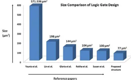
Figure-15 shows the reduction of size of the proposed structure with respect to the designs in reference paper. Younis et al. [11] proposed fully integrated OR and AND logic gate with size of 571.536 µm2, whereas our
proposed integrated all-optical OR logic gate structure has a compact size of 77 µm2. Comparatively our structure has
[image:5.612.77.291.346.477.2]a size reduction of almost 86.53%. The structure has very high speed response time of 150 fs. Both high speed operation and compact structure offers high speed laser based photonic integrated circuits for optical computing applications.
[image:5.612.72.297.538.655.2]Figure-15. Size comparison of logic gate design in various reference paper and the proposed structure.
Table-1. OR logic gate truth table with normalized transmitted power.
Input A Input B Normalized transmitted power
Output state
0 0 0 0
0 1 0.58 1
1 0 0.53 1
1 1 1.70 1
4. CONCLUSIONS
The silicon rods based 2D photonic crystal all-optical OR logic gate is designed and its logical operations are evaluated using FDTD and PWE method. OR logic operations are performed by incorporating the constructive beam interference effect in Y-type nonlinear photonic crystal. The FDTD method shows the visualization of
future optical integrated circuits and optical computing units with high speed laser signals. It also finds use in control and decision unit in the industrial and military application products.
REFERENCES
[1] J. W. M. Menezes, W. B. Fraga, A. C. Ferreira, K. D. A. Saboia, A. F. G. F. Filho, G. F. Guimarães, J. R. R. Sousa, H. H. B. Rocha, and A. S. B. Sombra, “Logic gates based in two and three-modes nonlinear optical fiber couplers,” Optical and Quantum Electronics, vol. 39, no. 14, pp. 1191-1206, (2007).
[2] K. S. Choi, Y. T. Byun, S. Lee, and Y. M. Jhon, “All-optical OR/NOR bi-functional logic gate by using cross-gain modulation in semiconductor optical amplifiers,” Journal of the Korean Physical Society, vol. 56, no. 4, pp. 1093-1096, (2010).
[3] Y. D. Wu, T. T. Shih, and M. H. Chen, “New all-optical logic gates based on the local nonlinear Mach-Zehnder interferometer,” Optics Express, vol. 16, no. 1, pp. 248-257, (2008).
[4] H.Z. Wang, W.M. Zhou and J.P. Zheng., “A 2D rods-in-air square-lattice photonic crystal optical switch”, International journal for light and electron Optics, (2010).
[5] Mohammad Ali Mansouri Birjandi and Majid Ghadrdan, “All-Optical Switch Based on Nonlinear Kerr Effect in Photonic Crystal Micro Ring Resonators”, International Journal of Natural and Engineering Sciences, vol. 7, no. 1, pp. 53-56, (2013).
[6] Wen-Piao Lin, Yu-Fang Hsu and Han-Lung Kuo, “Design of optical nor logic gates using two dimension photonic crystals”, American Journal of Modern Physics, vol. 2, no. 3, pp. 154-157, (2013).
[7] Rekha Mehra and Kajal Bhadel, “Design and Simulation of All-Optical OR Logic Gate based on 2-D Photonic Crystal”, International Journal of Computer Applications, vol. 99, no. 6, pp. 32-36, August (2014).
www.arpnjournals.com
[9] Gloria Joseph and Vijaylaxmi Kalyani, “Performance Analysis of 2D Photonic Crystal Optical Not Logic Gate”, International Journal Of Engineering Sciences and Research Technology, vol. 3, no.10, October (2014).
[10] X. Susan Christina and A. P. Kabilan, “Design of Optical Logic Gates Using Self-collimated Beamsin 2D Photonic Crystal”, Photonic Sensors, vol. 2, no. 2, pp. 173-179, (2012).