Citation:
Marino, MD and Weng, TH and Li, KC (2017) Exploiting Dynamic Transaction Queue Size in Scalable
Memory Systems. Soft Computing. ISSN 1432-7643 DOI:
https://doi.org/10.1007/s00500-016-2470-x
Link to Leeds Beckett Repository record:
http://eprints.leedsbeckett.ac.uk/3375/
Document Version:
Article
The aim of the Leeds Beckett Repository is to provide open access to our research, as required by
funder policies and permitted by publishers and copyright law.
The Leeds Beckett repository holds a wide range of publications, each of which has been
checked for copyright and the relevant embargo period has been applied by the Research Services
team.
We operate on a standard take-down policy.
If you are the author or publisher of an output
and you would like it removed from the repository, please
contact us
and we will investigate on a
case-by-case basis.
Exploiting Dynamic Transaction Queue Size in Scalable Memory Systems
Mario Donato Marino1, Tien-Hsiung Weng2, Kuan-Ching Li3
Abstract
In order to increase parallelism via memory width in scalable memory systems, a straightforward approach is to employ larger number of memory controllers (MCs). Nevertheless, a number of researches have pointed out that, even executing bandwidth-bound applications in systems with larger number of MCs, the number of transaction queue entries is under-utilized - namely as shallower transaction queues, which provides an opportunity to power saving. In order to address this challenge, we propose the use of transaction queues with dynamic size that employs the most adequate size, taking into consideration the number of entries utilized while presenting adequate levels of bandwidth and minimizing power. Experimental results show that, while saving up to 75% number of entries, the introduction of dynamic transaction queue mechanism can present savings up to 75% of bandwidth and 20% of rank energy-per-bit reduction compared to systems with 1-2ntries. With such promising results, it can be aimed and incorporated in modelling methodologies directed to the design and evaluation of new generation embedded systems.
Keywords: memory, controller, dynamic, transaction, queue, scalable.
1. Introduction
The increasing number of cores in current embed-ded and traditional multicore chip design has put an imprecendented high pressure on memory systems. As efforts to approach the I/O pin scalability - deter-minant factor of memory controller (MC) scalability, scalable memory systems utilize memory interfaces that allow I/O pin reduction and large-magnitude data rates to achieve MC scalability.
Double-data rate (DDR) memory is the most em-ployed dynamic memory system (DRAM) organi-zation in current multicore systems, where mem-ory DRAM chips share and enable address, decode, and I/O pins, and a memory rank, or simply rank -commercially called as dual inline memory module (DIMM). It is formed by several bank chips enabled in parallel, so that the total width is obtained when aggregating the width of each one of them. e.g., a 64-bit width is achieved by aggregating 8 banks of 8 bits. This context is illustrated in Figure 1.
Traditional Double-data rate (DDR) memory de-sign has been focused on memory frequency. That is,
Email address:[email protected],
[email protected], [email protected]
(Kuan-Ching Li )
1Leeds Beckett University (UK)
2Providence University (Taiwan)
3Corresponding Author, Providence University (Taiwan)
the application of higher clock frequencies to mem-ory formed by set of memmem-ory banks with data output aggregated and sharing addresses. Clock frequency scaling (FS) applied on these traditional systems have permitted DDR family generations been re-sponsible to bandwidth improvement. For instance, a factor of 10x larger clock frequencies has been applied along DDR family generations [1]. Since memory power usage is proportional to frequency, scalable memory systems also present the advantage of power, by shifting the traditional focus on FS to memory width, represented by MC and rank scala-bility, by assuming one rank for each MC or memory channel [2].
Comparatively to traditional solutions, advanced memory interfaces explore significant larger number of MCs, or MC counts. These advanced interfaces rely on optical- and radio-frequency (RF) technolo-gies that permit them to be implemented with fewer I/O pins, bringing out higher and optimized degrees of MC scalability. For instance, Corona is able to scale up to 64 optical-MCs [3] while DIMM Tree up to 64 RF-based memory controllers (RFMCs) [4].
[Figure 1 about here.]
transaction queue usage is reduced.
A number of researches present evaluations of most adequate size for transaction queues in terms of bandwidth and power [5]. Their evaluations are static ones, which do not take into consideration different transaction queue utilization rates along with the exe-cution of applications. Conditions for dynamic sizes are discussed in [5]; however, no algorithm, imple-mentation or evaluation of these dynamic sizes were analyzed. Therefore, a proper dynamic evaluation of the most appropriate transaction size is necessary to find the best power saving configuration that matches to the bandwidth utilization.
To advance the state-of-the art in scalable memory systems, we investigate in this paper the trade-offs of a dynamic transaction queue size to match the band-width utilization and minimize power comsumption, with the following contributions:
1. Design a dynamic transaction queue mecha-nism that matches to the number of entries uti-lized and memory load,
2. Create a model based on scalable memory sys-tems that has an inherent algorithm which dy-namically changes all transaction queue size to match the load. This proposed model is eval-uated using detailed and accurate simulation tools combined with memory bandwidth-bound benchmarks,
3. Perform evaluations on the proposed mecha-nism in terms of bandwidth impact under sev-eral workload conditions,
4. Evaluate rank power when utilizing dynamic transaction queues.
The remaining of this paper is organized as fol-lows. Section 2.2 and 3 presents the background and the related work respectively, and dynamic transac-tion queues are depicted in Sectransac-tion 4. Sectransac-tion 5 presents experimental results achieved, and finally, the concluding remarks and future directions are given in Section 6.
2. Background and Motivation
In this section, a bottom-up description of scalable memory systems by starting with the components of a memory rank and its operations/modes is provided. Following next, with the purpose of improving band-width and reducing latency as mentioned in previous section, we discuss scalable memory systems inter-faces that are able to scale ranks. Facts about how shallower transaction queues incur in the context of scalable memory system interfaces will also be de-picted.
Before we discuss how a rank is interfaced to RF circuits, we highlight that RFMCs are used instead of typical MCs. As reported in [2], RFMC is defined as a MC coupled to RF TX/elements that perform mod-ulation and demodmod-ulation of commands, data, clock, and addresses when performing memory operations (e.g., read and write). Signals are transmitted over the RF-interconnection between the RFMC and rank. Command, clock (CK), and address signals are de-modulated at the ranks, which also modulate data to be returned to the RFMC as a read operation per-formed. It is illustrated in Figure 2 the context where these previous memory path elements are employed. According to report [6], a typical MC is composed of elements, listed as: (a) front engine (FE), which processes L2 cache requests; (b) transaction engine (TE) that transforms these requests into control and data commands to be sent to the ranks, and (c) phys-ical transmission (PHY), composed by control / data physical channels. Particularly, along with its optical or RF memory interfaces, modulation and demodu-lation of commands, data, clock, and addresses are performed while executing typical read/write mem-ory operations. Along with these interfaces, signals are transmitted over the optical/RF interconnection between the optical-MC/RFMC and rank. Addition-ally, command, clock (CK) and address signals are demodulated at the ranks, as also modulate data to be returned to the MC when a read operation is per-formed. Figure 2 illustrates the context where the rank element is utilized together with an MC.
[Figure 2 about here.]
2.1. Scaling Memory Width - MC/rank scaling
In this subsection, we illustrate the performance and power motivations mentioned in previous sec-tions when scaling memory width and rank fre-quency as memory design techniques in scalable memory systems.
Memory width, represented by the total rank count width, it concurrently scales as rank count width are scaled. Despite that, memory width scalability is re-stricted by pin scalability, as indicated in [7][2].
Typical memory interface elements employed in scalable systems are exemplified in Figure 2, such
as DIMM Tree [4] and RFiof [2]. In these
sys-tems, RFMCs perform modulation of digital cache requests and demodulation of rank read
opera-tions. Similarly, ranks perform requests of write
[4] or the set formed by microstrips, microstrip-to-coaxial interface, and microstrip-to-coaxial cable in RFiof [2]. When an interposer is used in the motherboard im-plementation, RF elements can be placed.
By showing that RFpins are able to carry larger data rates, RFpin scalability is comparable to optical-pin one as depicted in [7][2], thus enabling RFMC scalability that support scalable systems and their scalable bandwidth.
As result, bandwidth achieved by scaling RFMCs is significantly higher than a typical 2-MC or 4-MC system employed in typical microprocessors [7][2][4]. For example, bandwidth achieved with 32 RFMCs in RFiof [2] is up to 7.2x higher than a 5-MC DDR-based system, assumed as a baseline in a 32-core processor configuration. Since bandwidth and latency are related based on Little’s law [8], latency is likely to decrease: a notable latency reduction of 69% is obtained in RFiof [2].
Another important advantage of these scalable
systems is power consumption. For example,
rank power consumption of RF-interface elements (TX/RX and RF-memory channel) correspond to 3-4% of a traditional DDR3 rank in DIMM Tree [4]. That is, at the same order of magnitude of a tra-ditional DDR3 rank. Furthermore, RFMCs can ar-chitecturally replace MCs, given their advantage in terms of power, as depicted in [7]. Given that larger bandwidths are achieved via employing larger num-ber of MCs, energy-per-bit is likely to decrease [2].
To illustrate the need for more MCs, the behavior of rank bandwidth along with different low power memory generations is shown in Figure 4 [1]. We could observe that total rank bandwidth is still re-stricted in terms of magnitude, a fact that motivates the need of approaching bandwidth via MC scalabil-ity.
[Figure 3 about here.]
Recently developed and commercially available memory solutions still employ larger number of pins that can still restrict MC scalability, i.e., memory width. For instance, Hybrid Memory Cube employs 55 pins and can utilize up to 8 MCs [9]. In ad-dition, the maximum aggregated bandwidth is 320 GB/s while each I/O-link presents individually 10 Gbit/s. Furthermore, Wide I/O 2 employs 128 bits per rank and 8 MCs, thus still MC-count restricted (total width 1024 bits) [10].
Another example of scalable solution is RFiof [2], illustrated in Figure 4b. RFiof is designed to scale to 32 RFMCs and 345.6 GB/s, using 10.8GB/s ranks. Given its lower number of pins and adoption of a conventional RF-interface (FR-board as in DIMM
Tree [4]), this technology has the potential to be scaled to make use of 64 RFMCs and ranks of 17.2 GB/s, to achieve the bandwidth of 1024GB/s (and total width of 4096 bits). The bandwidth magnitude achieved is similar by optical technologies [11][3].
2.2. Motivation
Each MC has a transaction queue, which is com-posed by certain number of entries utilized to store cache requests. As applications are executed, trans-action queue entries are filled depending on their memory-bound behavior. Applications with intense memory-bound behavior are likely to have more en-tries filled, and less enen-tries filled otherwise.
In scalable memory systems, sets of MCs and ranks are scaled to improve bandwidth and decrease power, whereas simultaneous memory transactions happens concurrently [3][7][2]. As one of motiva-tions mentioned in section , this increase in paral-lelism improves throughput and decrease latencies [7][2], yet shallowing transaction queue utilization, that signifies that less entries are utilized while faster processed when compared to typical systems (with low number of MCs available).
Going further, even in the scenario where intense memory-bound applications are executed, transac-tion memory queues are not completely utilized [7][2]. An example for intense memory-bound ap-plications are STREAM[12] and pChase[13], where the number of memory transactions entries occupied is reduced up to 5 times when scaling the number of MCs/ranks in RFiop [7] scalable memory system. In addition, the reports [14] [15] illustrate that intense memory-bound behavior can appear in other appli-cations such as in genetic algorithms where the ap-proach is via measuring the performance. The for-mer explores the conflicting input metrics, such as cost and power consumption, and produce a guide of an effective optimization to the multimedia embed-ded system designers. Another example of the ap-plications of these memory systems is likely to im-prove the performance of graphic processing units such as reported in [16] where a tree-based Genetic Programming could be utilized as a benchmark due to its bandwidth-bound behavior.
As conclusion from previous analysis, transaction queue entries are not completely occupied upon with memory requests, leading to its sub-utilization.
3. Related Work
im-proved performance and power implications of shal-lower transaction queues presented [5], by proposing a dynamic hardware approach that matches the trans-action queue size to behavior of applications.
Optical- [3] or RF-based solutions [7][2] utilize memory interface solutions to address the men-tioned I/O pin restrictions that permit MC scalabil-ity [11][2]. This approach can be applied to previ-ous scalable systems, matching the size of transac-tion queues to the size of the transactransac-tion tuned to the application executed.
With the challenges induced by growing num-ber of cores in the multicore era, Udipi [11] pro-posed a number of hardware and software mech-anisms to approach higher memory bandwidth de-mands via utilization of optical-based interfaces, ap-propriate memory organization for taking advantage of optical transmission, and MC optimizations to im-prove power and performance. Notwithstanding, this study focused on proposing a dynamic technique that allows to explore the lower utilization of transaction queues in scalable optical and RF memory interfaces. In the report by Jeong et al. [17] a Quality of Service (QoS) mechanism to track progress of GPU workload is proposed in order to dynamically adapt the priority of CPU and GPU utilization. The re-port by Usui et al.[18] extends Jeong’s approach [17] to general hardware accelerators trading off not only QoS bandwidth but also latency of applications. Dif-ferently of the GPU or CPU priority - focus of these QoS reports - in this study, we approach to dynam-ically adapt the transaction queue size to match the application.
Janz et al. [19] report employs a software schedul-ing software framework where through the interac-tion of the operating system with the applicainterac-tion, memory address space dynamic footprint utilization is determined. Our technique is a hardware technique that could be orthogonally coupled to Janz’technique and also collaborate to determine the memory foot-print utilization of the system in terms of transaction queue size.
Since the adopted approach is focused on transac-tion queues, it is orthogonal to optical or RF-based solutions, and therefore, applicable to these systems. The strategy here proposed is also suitable to com-mercial systems such as HMC [9] with medium
de-gree of MC scalability. Additionally, transaction
queue occupation is decreased in RFiop [7] as MCs are scaled. This observation is a motivation to further explore the behavior of shallower transaction queues in this research.
Memscale [20] is a set of software (operating sys-tem policies) and specific hardware power
mecha-nisms that enable the trade-off between memory en-ergy and performance in typical memory systems. It dynamically changes voltage and frequency scal-ing (DVFS) in terms of memory ranks and mem-ory channels. Moreover, it is guided by OS per-formance counters that periodically monitor mem-ory bandwidth usage, energy utilization, and the de-gree of performance degradation in the case of trade-off. The proposed approach is orthogonal to Mem-scale, since the impact on the reduction of transaction queues in terms of power and bandwidth is dynami-cally explored, which can be triggered by Memscale techniques. What we propose is also orthogonal to the report by Marino [21] since we do not explore transaction queue FS, instead the focus is on saving energy by having dynamic number of buffers adapt-able to the memory demand.
Multiscale [22] technique relies on the approach that estimates the bandwidth of each MC indepen-dently and selects an appropriate frequency/voltage to maximize energy savings while individually max-imize the performance of each application. In this proposed research, we aim to employ the lower uti-lization of transaction queues through the use of a dy-namic strategy that automatically fits the number of entries to the application bandwidth demands. Simi-lar to Memscale, this proposed technique can be cou-pled to Multiscale due to their orthogonality.
Howardet al.[23] proposed memory DVFS to
ad-dress memory power at data centers using bandwidth as a restricting factor. Although the proposed ap-proach is orthogonal to this study, given that we fo-cus on evaluating the benefits of shallower transac-tion queues, a combined approach DVFS applied to the transaction queue is an issue for further investi-gation.
In [24], it was proposed an architecture of servers with mobile memory systems for lower energy-per-bit consumption and efficient idle modes to ap-proach different energy utilization under different bandwidth demands, which can be applied in servers with mobile systems that present larger number of MCs. As part of this research, it is shown the use of mobile memories with new circuitry to reduce power. In addition, orthogonal to the study presented in [24], we focused on the effects of using shallower transac-tion queues.
Scale-Out Non Uniform Memory Access
even for MCs located in remote positions from the processor whilst have significant lower levels of latency. It can potentially explore remote locations that shows higher latencies and a strategy is pro-posed in this research that will further lower their utilization.
Zhang et al. [26] proposes the utilization of a
variation-aware MC scheme that explores the utiliza-tion of memory chunks within different access times. The approach proposed in this work is similar, since it explores lower bandwidth utilization of transaction queue. Nevertheless, frequency scaling is one of the main techniques explored in [26], and lowering the number of transaction queues is explored to match the demands on the bandwidth.
ArchShield [27] is an architectural framework that employs runtime testing to identify faulty DRAM cells. Similar to ArchShield that exposes errors at ar-chitecture level, our region-based approach can po-tentially tolerate regions with faulty DRAM cells. Rather than focusing on banks and internal cell lev-els to approach error-tolerance, the approach pro-posed in this work is focused on the rank and MC levels, where the performance and energy implica-tions of regions formed by sets of cores and differ-ent number of MCs/ranks, given that latter one rep-resent different degrees of memory parallelism.
Sim-ilar to ArchShield [27], Taassoriet al.[28] proposed
an adaptive MC that retains information of each in-dividual bank, in which DVFS is gradually applied and seeks to find the point of failure (clock synchro-nization) in these banks. Intersecting with Taassori et al.is the granularity at the memory element level, where differences in fabrication variation are utilized to exploit FS independently at each different memory element. Lower utilization of transaction queues of MCs is explored to satisfy different bandwidth de-mands in this investigation.
Bandwidth effects of increasing the number of MCs in traditional digital-based embedded systems is presented in [16], restricted due to high I/O pin usage. One of the effects observed was the lower utilization of transaction queues, where the proposed approach focuses using transaction queues with dy-namic sizes that match the bandwidth demands.
The effects of shallower transaction queues is dis-cussed in [5], where the number of MCs is increased, concurrently the occupation of the queues is lowered. As consequence, many entries are not utilized. To further approach the utilization of these queues, the proposed research matches the current bandwidth via a dynamic approach.
4. Dynamic Transaction Queues Size Mechanism
Before we describe the dynamic transaction queue mechanism, we illustrate first the general operation of transaction queues.
while(there are incoming memory transactions
)do
if(checkM T QS)then
activate entry(tqc); incrementtqc;
end end
while(there are memory transactions to be
removed)do
if(tqc >= 0)then
de-activate entry(tqc); decrementtqc;
end end
Algorithm 1: Dynamic transaction queue size
mechanism algorithm:tqcis assumed starting with
0
4.1. Transaction Queue operation
The transaction queue is typically involved when one cache request is received from the cache system and transformed next into a memory request in the TE (MC), as previously described. In scalable mem-ory systems, typical transaction queue sizes are in the range of 16-32 entries [5], and one memory re-quest occupies one entry in the transaction queue. While the memory is still processing this request, this entry is kept occupied. Transaction queues store cache requests and transform into memory requests are queued due to speed difference between caches and DRAMs.
After processing the request, the entry correspon-dent to the stored memory request is freed from the transaction queue. Given that transaction queue en-tries correspond to the maximum transaction queue size, all queue entries are free, since no memory re-quests are on the way nor rere-quests being processed.
completed, the correspondent transaction queue en-try is released and the number of available entries is further incremented by one.
4.2. Mechanism
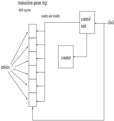
In order to improve the sub-utilization of trans-action queues [5], a dynamic transtrans-action queue size mechanism is proposed. Since this algorithm 1 being proposed is aimed to be implemented in hardware, it should be of smallest complexity overhead, mainly consisted of simple operations such as activation/de-activation of entries that indirectly control transac-tion queue size. To implement this mechanism, it is proposed:
• add a counter (transaction queue counter or
tqc), to represent the number of entries utilized
in the transaction;
• novel design of a queue that has several entries
is considered instead of using a traditional trans-action queue: it will control the activation/de-activation of each of active entries, due to power saving issues.
[Figure 4 about here.]
The hardware kernel of the proposed mechanism should control the number of entries available, de-pending on the current number of transactions stored in the TE transaction queue. As one new transaction incomes to the transaction queue and there are en-tries available, the transaction is stored in the queue and concurrently the transaction entry is occupied with this respective memory request. Once checked the availability of entries, whether maximum
trans-action queue size or M T QS has achieved or not,
the dynamic transaction queue mechanism performs
the correspondent hardware adjustment: tqc is
in-cremented by one and one more entry is activated (activate entry) next. In comparison to the tradi-tional queue mechanism where all entries are acti-vated even not used, only used entries are actiacti-vated and no idle entries in this case.
In similar way, the correspondent entry is removed from the transaction queue after the transaction is processed. Dynamic transaction queue mechanism performs the adjustment of the transaction queue
size: the correspondent entry is de-activated (de−
activate entry) andtqcis decremented by one. Dif-ferent than the traditional queue mechanism where all entries are activated even if not used, only used entries are active and no idle entries in this case.
The operations of checking the transaction queue
size (check M T QS) and verification of entries to be
processed both can be implemented using circuits. The circuits needed to implement the dynamic trans-action queue mechanism are straightforward
com-parator circuits and counters. The complexity of
the circuits involved in this mechanism is not high in terms of overall processor/memory circuits com-plexity. Yet, not likely to impact power utilization. Therefore, if these circuits need to be scaled to 32 or even 64 entries, the area and power utilized are still neglectable.
The transaction queue implementation itself can be done through a shift-register element. That is, as a new entry is stored, the shift-register and transaction counter are properly clocked to respectively store the entry and then count it. The activation and de-activation of entries are assumed to be implemented through coupling power-gating inputs to the entries, which allows them to be enabled or disabled when-ever a number or no entries are necessary.
Since the number of active entries is significant lower than the maximum [5], power benefits can be noticed as further described in Section 5.
[Table 1 about here.]
5. Experimental Results
In this section, experiments were executed to demonstrate the power and performance effects, with different transaction queue sizes in scalable memory systems.
5.1. Methodology
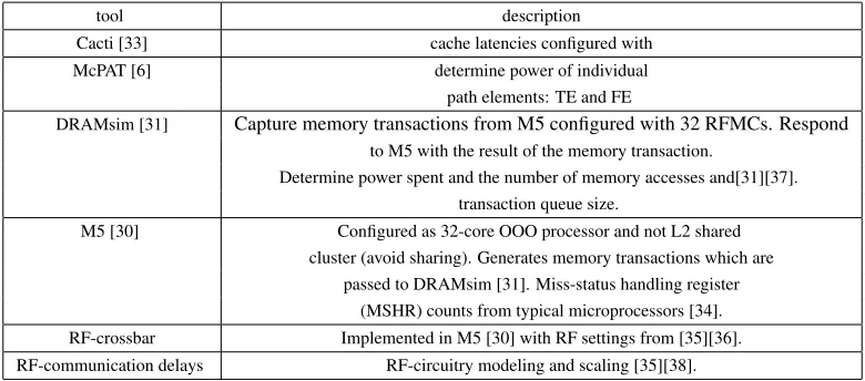
To have a global picture of the methodology ap-plied in this research, we list simulators considered and corresponding description of their
characteris-tics, available in Table 1. The methodology
em-ployed to obtain bandwidth is adopted based on [29]. That is, by using bandwidth-bound benchmarks to stress the memory system, M5 [30] and DRAMsim [31] simulators were combined.
MC ratio is homogeneous, i.e., 32:32. DRAMsim responds to M5 with the result of each memory trans-action concurrently in the sequence. In this way, each RFMC is assumed to be connected to one single rank to extract its maximum bandwidth.
To evaluate the dynamic behavior, its behavior is compared to the behavior of other transaction queue sizes (from 1 to 16 entries) obtained via static design space exploration, taking into consideration band-width and rank-energy-per-bit utilization. The base-line configuration presents 32 RFMCs and 16 trans-action queue elements.
[Table 2 about here.]
We employ a 4.0GHz (Alpha ISA) and 4-wide out-of-order (OOO) core, with RFMCs at 2.0GHz (typically at half of microprocessor clock frequency [32]). Cacti [33] is chosen to acquire cache laten-cies and adopt MSHR counts of typical microproces-sors [34]. L2 caches at 1 MB/core are interconnected via an 80GB/s-RF-crossbar with 1-cycle latency are adopted. This magnitude was designed so that when ranks and MCs are scaled, it does not restrict the total throughput. Same timing settings adopted as those presented in [35][36]. RF-crossbar was set with a single cycle latency, adopted the same timing set-tings as in [4]. That is, 200ps for TX-RX delays plus the rest of the burst cycle used to transfer 64 Bytes (memory word) using high speed and modulation.
Observing the RF-crossbar upper constraint, we have selected a medium data-rate DDR3-rank em-ployed in typical PCs (64 data bits, based on the DDR3 model Micron MT41K128M8 of 1GB [37], and listed in Table 2a). All architectural parameters are summarized in Table 2a.
To model RF communication, RF-circuitry mod-eling and scaling took into consideration those pro-posed in [35][38][36][39]. In these models, crosstalk effects, modulation, interference, and noise margin reduction are employed aiming at low bit error rate (BER). Moreover, these models are validated with prototypes for different transmission lines [40][38], following ITRS [41]. RF-interconnection power is derived as in [2]; that is, using McPAT [6] tool at dif-ferent frequencies to determine FE/TE power com-ponents and RF-interconnection power modeling as in [4].
To determine the total energy-per-bit spent, DRAMsim power infrastructure is employed and then combine it to the memory throughput, as ex-tracted from M5 statistics (ratio of the number of memory transactions and execution time).
[Figure 5 about here.]
By adopting methodology similar to the one proposed to evaluate the memory system [34], bandwidth-bound benchmarks with a medium-to-significant number of misses per kilo-instructions (MPKI) were selected, taking into consideration the following aspects:
• Guarantee proper calibration by having each
rank bandwidth saturated. In all benchmarks, more than one entry is present at each trans-action queue of each MC, what guarantees that bandwidth in each rank is saturated.
• The selected input sizes are a trade-off between
simulation times and memory traffic generated.
• In high scalable memory systems, typically at
least 16 entries per transaction queue are uti-lized [4][7][2]. Thus, the baseline reference of the results presented is the 16-entry one (trans-action queue with 16 entries).
In order to evaluate this scalable memory system, we have selected seven bandwidth-bound bench-marks: (i) STREAM suite [12], composed of ADD, COPY, SCALE and TRIAD benchmarks, (ii) pChase [13] with pointer chase sequences randomly ac-cessed, (iii) Multigrid (MG), Scalar Pentadiago-nal (SP), Fast Fourier Transform (FFT) from NPB benchmarks [42], and SOR method (black and red matrices) [43]. All benchmarks are set to make use 32 threads, since we are employing a 32-core pro-cessor. No special thread-to-core mapping is applied when executing these benchmarks. Table 2b lists the benchmarks experimented, input sizes, read-to-write rate, and L2 MPKI obtained from experiments. In all benchmarks, parallel regions of interest are executed until completion, and input sizes guarantee that all memory space used is evaluated. Average results are calculated based on harmonic average.
5.2. Experimental Results
In this section, we present the results regarding to the aspects of memory bandwidth and rank energy-per-bit magnitude. Since all STREAM benchmarks belong to the same STREAM suite, instead of pre-senting four benchmarks they are presented alto-gether as STREAM.
evaluated. As result, the algorithm allows the uti-lization of lower number of entries when compared to 16 entries, which corresponds to the baseline - as previously described and used in scalable memory systems [7][2].
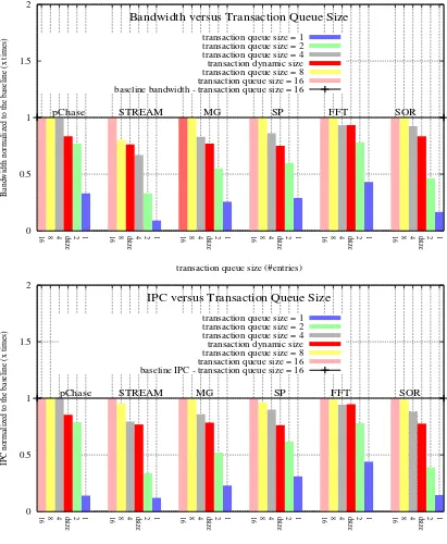
Figure 5a illustrates experimental results on band-width. The dynamic version presents an expected bandwidth magnitude, i.e., with magnitude levels within the 16-1 range entry, the latter ones obtained with experiments of individual sizes. As expected, since the dynamic transaction queue tries to optimize the utilization of the transaction queue and employs less elements than the total size (16 elements, set as baseline as discussed previously), bandwidth lev-els are lower than the baseline yet better than small sizes, e.g., 2-4 or 4-8 entries. For STREAM and FFT, dynamic version present higher bandwith than the 4-entry version. For the remaining benchmarks it presents 2 to 8% less bandwidth, which is a yet open trade-off for having lower transaction queue size (and power reduction at the MC).
The point where bandwidth starts to be signif-icantly reduced happens with 4 transaction queue
sizes [5]. Indeed, this point corresponds to the
dynamic approach matching the bandwidth needs, given the number of entries available, memory be-havior of the benchmark, cache L2 MSHRs, and/or number of outstanding memory transactions.
Before the discussing rank energy-per-bit levels, processor performance impact (in terms of IPC) is shown in Figure 5b. IPCs generally follow the be-havior of bandwidth as previously described. Most interestingly, it is noted that the IPC magnitude level for the obtained through dynamic transaction queue algorithm is less than the one obtained when band-width is comparatively measured. Therefore, in spite of using bandwidth, IPC/bandwidth trade-off could be considered to trigger the algorithm.
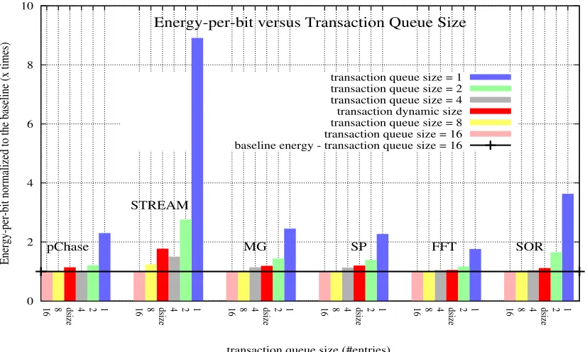
It is illustrated the related rank energy-per-bit re-sults in Figure 6. The dynamic version present simi-lar rank energy-per-bit levels to the 4-entry system, except for STREAM where levels are larger than 4- and 8-entry. Similar to the 4-entry version, the dynamic transaction queue version presents lower energy-per-bit levels than for 1-2 entries. Analyzing the simulator output statistics, it is believed that such event happens due to random behavior settings of pChase. We observe different energy-per-bit magni-tudes from [5], since we believe the latter calculated and compared The general behavior which is energy-per-bit levels to proportionally increase with lower transaction-queue size is expected since lower trans-action queues are likely to present lower bandwidth, and higher latency, i.e., longer times and therefore
higher energy utilization.
By combining energy and bandwidth aspects, if such a trade-off bandwidth drop of about 25% is ac-ceptable, this implies that 50% to 75% of transaction queue entries are not be used, what lead to signifi-cant transaction queue power savings. In this case, as observed in the sequence, rank energy-per-bit can be saved of about 20% whilst using less amount of transaction queue positions and saving power.
[Figure 6 about here.]
To summarize, it is shown interesting trade-offs of dynamic configurations in terms of band-width/performance and energy while employing less amount of elements, by comparing Figures 5a, 5b and 6. It is able to observe that is possible to have equivalent performance to 16 entries while present-ing potential energy-per-bit savpresent-ing with 4 and 8 en-tries, less than 50% of the total number of entries.
Importantly, we do not show the dynamic transac-tion queue energy utilizatransac-tion. However, as a result of the target technique, given that the bandwidth and IPC results of the dynamic queue are similar to the 4-entry system, the energy utilization is likely to fol-low this behavior: if compared to the 16-entry base-line is likely to use 4x more energy. So a trade-off memory energy utilization versus transaction queue utilization should be explored to clarify this behav-ior, which We leave as a further investigation. aspect as a future investigation.
6. Conclusions and Future Plans
One of consequences on employing scalable mem-ory interfaces that has larger number of MCs is the decrease on the number of entries utilized in trans-action queues. In this paper, we have proposed a mechanism that dynamically matches the number of entries utilized to the number of entries demanded by programs. Evaluations on the bandwidth and im-pact of power when performing dynamic transaction queue size implementation in the context of scalable memory systems are done.
higher number of MCs to higher number of entries are likely solutions to be further investigated.
Moreover, the dynamic solution trade-off perfor-mance and energy losses are small if compared to 4-to-16 entries. A further investigation is required to expand the boundaries of the trade-off.
As future directions, we aim to investigate vari-ations of the dynamic approach that includes pro-cessor utilization and others [20][21] that take into consideration factors as bandwidth solely. Methods that combine DVFS [23], temperature, processor to memory locality (important to distributed memory systems) and other memory traffic patterns are listed as directions to be considered.
Similar investigation would be interesting to be applied on the context of BD clusters with embedded systems’ features [44] with detailed design choices and optimizations are performed by decomposing the global system into a set of simple [45] and
well-described components. Modelling methodologies
based on data analysis that characterizes the perfor-mance of embedded applications are applied to sup-port system-level designers to predict the number of execution cycles on a embedded processor [46]. As basis of a high-level characterisation on the software functionality and hardware architecture, we aim fur-ther to include the findings of this methodology in system research studies.
7. Compliance with Ethical Standards:
(In case of Funding) Funding: This study was funded by X (grant number X).
Conflict of Interest: Author A has received search grants from Company A. Author B has re-ceived a speaker honorarium from Company X and owns stock in Company Y. Author C is a member of committee Z. OR if no conflict exists: Author A de-clares that he/she has no conflict of interest. Author B declares that he/she has no conflict of interest.
(In case animals were involved) Ethical approval : All applicable international, national, and/or institu-tional guidelines for the care and use of animals were followed.
(And/or in case humans were involved) Ethical ap-proval: All procedures performed in studies involv-ing human participants were in accordance with the ethical standards of the institutional and/or national research committee and with the 1964 Helsinki dec-laration and its later amendments or comparable eth-ical standards.
(If articles do not contain studies with human par-ticipants or animals by any of the authors, please
select one of the following statements) Ethical ap-proval: This article does not contain any studies with human participants performed by any of the authors. (Or) Ethical approval: This article does not contain any studies with animals performed by any of the au-thors. (Or) Ethical approval: This article does not contain any studies with human participants or ani-mals performed by any of the authors.
(In case humans are involved) Informed consent: Informed consent was obtained from all individual participants included in the study.
8. Bibliography
[1] LPDDR4 Moves Mobile, mobile Forum
2013, presented by Daniel Skinner,
Ac-cessed date: 01/27/2016; http://www.
jedec.org/sites/.../D Skinner Mobile Forum May 2013 0.pdf.
[2] Marino, M. D., RFiof: An RF approach to the I/O-pin and Memory Controller Scalability for Off-chip Memories, in: CF, May 14-16 , Ischia, Italy, ACM, 2013, pp. 100–110.
[3] D. Vantrease et al, Corona: System Implica-tions of Emerging Nanophotonic Technology, in: ISCA, IEEE, DC, USA, 2008, pp. 153–164. [4] Therdsteerasukdi, Kanit et al., The DIMM tree architecture: A high bandwidth and scalable memory system, in: ICCD, IEEE, 2011, pp. 388–395.
[5] Marino, M.D; Li K.C., Implications of Shal-lower Memory Controller Transaction Queues in Scalable Memory Systems, Journal of Super-computing.
[6] Sheng Li et al, McPAT: an integrated power, area, and timing modeling framework for
mul-ticore and manycore architectures, in:
MI-CRO’09, ACM, New York, USA, 2009, pp. 469–480.
[7] Marino, M. D., RFiop: RF-Memory Path To Address On-package I/O Pad And Memory Controller Scalability, in: ICCD, 2012, Mon-treal, Quebec, Canada, IEEE, 2012, pp. 183– 188.
[8] Little, J. D. C. (1961). ”A Proof for the
Queuing Formula: L = W”. Operations
Research 9 (3): 383387., accessed date:
11/08/2016 ; http://dx.doi.org/10.
[9] Hybrid Memory Cube Specification
1.0, accessed date: 09/12/2016 ;
http://www.hybridmemorycube.org/.
[10] JEDEC Publishes Breakthrough Standard for Wide I/O Mobile DRAM, accessed date: 11/03/2016 ; http://www.jedec.org/.
[11] Aniruddha N. Udip, Designing Efficient Mem-ory for Future Computing Systems , in: PhD Thesis, University of Utah, School of Comput-ing, Utah, USA, 2012, pp. 1–126.
[12] McCalpin, J. D., Memory Bandwidth and Ma-chine Balance in Current High Performance Computers, IEEE TCCA Newsletter (1995) 19–25.
[13] The pChase Memory Benchmark Page, ac-cessed date: 10/05/2016 ; http://pchase.org/. [14] Bruno Nogueira et al., Multi-objective
opti-mization of multimedia embedded systems us-ing genetic algorithms and stochastic simula-tion, Soft Computing.
[15] Darren M. Chitty, Improving the performance GPU-based genetic programming through ex-ploitation of on-chip memory, Soft Computing 20 (2) (2016) 661–680.
[16] Marino, M. D., Li, K.C., Insights on Mem-ory Controller Scaling in Multi-core Embedded Systems , International Journal of Embedded Systems 6 (4).
[17] M. K. e. a. Jeong, A qos-aware memory con-troller for dynamically balancing gpu and cpu bandwidth use in an mpsoc, in: DAC, ACM, New YorkUSA, 2012, pp. 850–855.
[18] SQUASH: Simple QoS-Aware
High-Performance Memory Scheduler for
Het-erogeneous Systems with Hardware
Ac-celerators, accessed date: 10/02/2016 ;
http://http://arxiv.org/abs/1505.07502.
[19] J. M. R. et al., A framework for application guidance in virtual memory systems, in: VEE, ACM, 2013, pp. 344–355.
[20] Deng, Q. et al., Memscale: active low-power modes for main memory, in: Proceedings of the Sixteenth ASPLOS, ACM, New York, NY, USA, 2011, pp. 225–238.
[21] Marino, M.D., ABaT-FS: Towards adjustable bandwidth and temperature via frequency scal-ing in scalable memory systems, Microproces-sors and Microsystems.
[22] Deng, Q. et al., Multiscale: Memory system dvfs with multiple memory controllers, in: Pro-ceedings of the 2012 ACM/IEEE International Symposium on Low Power Electronics and De-sign, ISLPED ’12, ACM, New York, NY, USA, 2012, pp. 297–302.
[23] David et al., Memory Power Management via Dynamic Voltage/Frequency Scaling, in: Pro-ceedings of the 8th ACM International Con-ference on Autonomic Computing, ICAC ’11, ACM, New York, NY, USA, 2011, pp. 31–40. [24] Malladi et al, Towards Energy-proportional
Datacenter Memory with Mobile DRAM, in: Proceedings of the 39th Annual International Symposium on Computer Architecture, ISCA ’12, IEEE Computer Society, Washington, DC, USA, 2012, pp. 37–48.
[25] Novakovic, Stanko et al., Scale-out NUMA, in: Proceedings of the 19th International Con-ference on Architectural Support for Program-ming Languages and Operating Systems, AS-PLOS ’14, ACM, New York, NY, USA, 2014, pp. 3–18.
[26] Zhang, Xianwei et al., Exploiting dram restore time variations in deep sub-micron scaling, in: Proceedings of the 2015 Design, Automation & Test in Europe Conference & Exhibition, DATE ’15, San Jose, CA, USA, 2015, pp. 477– 482.
[27] Nair, Prashant J. et al., ArchShield: Architec-tural Framework for Assisting DRAM Scal-ing by ToleratScal-ing High Error Rates, in: Pro-ceedings of the 40th Annual International Sym-posium on Computer Architecture, ISCA ’13, ACM, New York, NY, USA, 2013, pp. 72–83. [28] Taassori M. et al., Exploring a Brink-of-Failure
Memory Controller to Design an Approximate Memory System, in: 1st Workshop on Ap-proximate Computing Across the System Stack (WACAS), ACM, Salt Lake City, 2014, pp. –. [29] Marino, M. D., On-Package Scalability of RF
and Inductive Memory Controllers, in: Euromi-cro DSD, IEEE, 2012, pp. 923–930.
[30] Nathan L. Binkert et al, The M5 Simulator: Modeling Networked Systems, IEEE Micro 26 (4) (2006) 52–60.
[31] David Wang et al, DRAMsim: a memory
[32] AMD Reveals Details About Bulldozer
Mi-croprocessors, accessed date: 09/06/2016
-http://www.xbitlabs.com/news/cpu/display/ 20100824154814 AMD Unveils Details About
Bulldozer Microprocessors.html (2011).
[33] CACTI 5.1, accessed Date: 10/22/2016;
http://www.hpl.hp.com/techreports/2008/HPL-200820.html.
[34] Loh, Gabriel H., 3D-Stacked Memory Archi-tectures for Multi-core Processors, in: ISCA, IEEE, DC, USA, 2008, pp. 453–464.
[35] M. Frank Chang et al, CMP Network-on-Chip Overlaid With Multi-Band RF-interconnect, in: HPCA, 2008, pp. 191–202.
[36] M.C.F. Chang et al., Power reduction of CMP communication networks via RF-interconnects, in: MICRO, IEEE, Washington, USA, 2008, pp. 376–387.
[37] Micron manufactures DRAM components and modules and NAND Flash, accessed date: 01/08/2016 ; http://www.micron.com/.
[38] M.C.F. Chang et al, Advanced RF/Baseband In-terconnect Schemes for Inter- and Intra-ULSI Communications, IEEE Transactions of Elec-tron Devices 52 (2005) 1271–1285.
[39] Sai-Wang Tam et al, RF-Interconnect for Fu-ture on-Chip, Low Power Network-on-Chip (2011) 255–280.
[40] G. Byun et al, An 8.4Gb/s 2.5pJ/b Mobile Memory I/O Interface Using Bi-directional and Simultaneous Dual (Base+RF)-Band Signal-ing, in: ISSCC, IEEE, 2011, pp. 488,490.
[41] ITRS HOME, accessed date: 08/18/2016 ;
http://www.itrs.net/.
[42] NAS Parallel Benchmarks,
ac-cessed date: 08/09/2016;
http://www.nas.nasa.gov/Resources/Software /npb.html/.
[43] R. G. Rauber T., Parallel programming: for multicore and cluster systems, 2nd Edition, Springer, 2013.
[44] Marino, M.D; Li K.C., Last level cache size heterogeneity in embedded systems, Journal of Supercomputing 72 (2) (2016) 503–544.
[45] Marino, M.D, L2-Cache Hierarchical Organi-zations for Multi-core Architectures, in: Fron-tiers of High Performance Computing and Net-working – ISPA 2006 Workshops: ISPA 2006 International Workshops, FHPCN, XHPC, S-GRACE, GridGIS, HPC-GTP, PDCE, ParDM-Com, WOMP, ISDF, and UPWN, Proceedings, Springer, 2006, pp. 74–83.
[46] G. Bontempi , W. Kruijtzer, The use of intelli-gent data analysis techniques for system-level design: a software estimation example, Soft Computing 8 (7) (2004) 477–490.
[47] Calculating Memory System Power for DDR3
Introduction, accessed date: 12/06/2015 ;
List of Figures
1 memory system general overview . . . 13
2 (16384 rows, 128 columns, 64 data bits) rank interfaced to a RF-based MC; based on [2][47] 14
3 left to right: (a) frequency versus bandwidth, repeated from [1]; (b) RFiof, repeated from [2] 15
4 transaction queue circuits . . . 16
5 a and b: top to bottom, bandwidth and instructions-per-cycle (IPC) for STREAM, pChase,
MG, SP, FFT and SOR . . . 17
...
rank
[image:14.612.89.531.69.296.2]rank
... ...
...
row decoder
mux
sense amplifiers
column mux
bank
rank DRAM chip
memory array
MC MC MC
multicore
processor
optical or RF interconnection
data/address/command modulated signals
CKE clock
demodulate register address
refresh counter
sense amplifiers bank0 memory array (16384 x 128 x 64) 16384
I/O gating
column decoder
read latch
MUX 64
receiver 8 A0−A13
BA0−BA2 command
.
8192
input registers
write drivers control
logic
.
drivers
.
counter address latch column control bank logic MUX address row demodulate
demodulate modulate/ DM
DQS−DQS# DQ0−DQ7 RF−interconnection
RF−interconnection
Rank interfaced to RF TX/RX
RFMC
Delay locked loop (DLL)
64 demodulate
modulate/
128 bank0
row− address latch & decoder
[image:15.612.135.478.257.520.2]. ..
.. .
...
...
trench
...
L1microstrip and trench other than I/O pad connected to MCs solder ball
top surface mettalurgy power and ground planes coaxial cable DRAM RX/TX substrate package trace not connected to MCs
RFpin
substrate
coaxial cable RFMC
microstrip and trench
L2 L1 core
processor package
RX/TX
mshr
core die
memory package
DRAM rank
die
memory
substrate cont
PCB
PCB
core/L1
core/L1 L2
L2 RFMC
floorplan
processor package
RFMC
RX/TX
RX/TX
DRAM rank memory package DRAM rank
package memory
coaxial cable coaxial
cable trench trench microstrip
microstrip
[image:16.612.92.521.70.327.2]RFpin
RFpin
entries
transaction queue (tq):
shift registerenable and /enable
control
unit
counter
[image:17.612.184.423.72.327.2]clock
0 0.5 1 1.5 2
16 8 4 dsize 2 1 16 8 dsize 4 2 1 16 8 4 dsize 2 1 16 8 4 dsize 2 1 16 8 4 dsize 2 1 16 8 4 dsize 2 1
Bandwidth normalized to the baseline (x times)
transaction queue size (#entries)
Bandwidth versus Transaction Queue Size
transaction queue size = 1 transaction queue size = 2 transaction queue size = 4 transaction dynamic size transaction queue size = 8 transaction queue size = 16 baseline bandwidth - transaction queue size = 16
pChase STREAM MG SP FFT SOR
0 0.5 1 1.5 2
16 8 4 dsize 2 1 16 8 4 dsize 2 1 16 8 4 dsize 2 1 16 8 4 dsize 2 1 16 8 4 dsize 2 1 16 8 4 dsize 2 1
IPC normalized to the baseline (x times)
transaction queue size (#entries)
IPC versus Transaction Queue Size
transaction queue size = 1 transaction queue size = 2 transaction queue size = 4 transaction dynamic size transaction queue size = 8 transaction queue size = 16 baseline IPC - transaction queue size = 16
[image:18.612.96.507.76.576.2]pChase STREAM MG SP FFT SOR
0 2 4 6 8 10
16 8 dsize 4 2 1 16 8 dsize 4 2 1 16 8 4 dsize 2 1 16 8 4 dsize 2 1 16 8 4 dsize 2 1 16 8 4 dsize 2 1
Energy-per-bit normalized to the baseline (x times)
transaction queue size (#entries)
Energy-per-bit versus Transaction Queue Size
transaction queue size = 1 transaction queue size = 2 transaction queue size = 4 transaction dynamic size transaction queue size = 8 transaction queue size = 16 baseline energy - transaction queue size = 16
pChase
STREAM
[image:19.612.96.508.76.324.2]MG SP FFT SOR
List of Tables
1 methodology: tools and description . . . 20
tool description
Cacti [33] cache latencies configured with
McPAT [6] determine power of individual
path elements: TE and FE
DRAMsim [31] Capture memory transactions from M5 configured with 32 RFMCs. Respond
to M5 with the result of the memory transaction.
Determine power spent and the number of memory accesses and[31][37]. transaction queue size.
M5 [30] Configured as 32-core OOO processor and not L2 shared
cluster (avoid sharing). Generates memory transactions which are passed to DRAMsim [31]. Miss-status handling register
(MSHR) counts from typical microprocessors [34].
RF-crossbar Implemented in M5 [30] with RF settings from [35][36].
[image:21.612.111.501.70.242.2]RF-communication delays RF-circuitry modeling and scaling [35][38].
Core 4.0 GHz, OOO, multicore, 32 cores, 4-wide issue, turnament branch predictor
Technology 22 nm
L1 cache 32kB dcache + 32 kB icache;
associativity = 2 MSHR = 8, latency = 0.25 ns
L2 cache 1MB/per core ; associativity = 8
MSHR = 16; latency = 2.5 ns
RF-crossbar latency = 1 cycle, 80GB/s
RFMC 32 RFMCs; 1 RFMC/core,
2.0GHz, on-chip
trans. queue entries = 16/MC,
close page mode
Memory rank DDR3 1333MT/s,
1 rank/MC, 1GB, 8 banks, 16384 rows, 1024 columns, 64 bits,
Micron MT41K128M8 [37], tras=26.7cycles, tcas=trcd=8cycles RF
interconnection
length size 2.5 cm
delay 0.185ns
Benchmark Input Size read : write MPKI
Copy, Add, 4Mdoubles per 2.54:1 54.3
Scale, core
Triad 2 interations
(STREAM)
pChase 64MB/thread, 158:1 116.7
3 iterations, random
Multigrid:MG Class B 76:1 16.9
(NPB) 2 iterations
Scalar Class B 1.9:1 11.1
Pentadiagonal:
SP (NPB) 2 iterations 1.9:1 11.1
FFT: Fast Class B, 1.3:1 6.8
Fourier 3 iterations
Transform (NPB) (NPB)
[image:22.612.88.536.245.529.2]SOR 6000 x 6000, 3 iter. 2.5:1 12.5
![Figure 2: (16384 rows, 128 columns, 64 data bits) rank interfaced to a RF-based MC; based on [2][47]](https://thumb-us.123doks.com/thumbv2/123dok_us/16735.1002077/15.612.135.478.257.520/figure-rows-columns-data-bits-interfaced-based-based.webp)
![Figure 3: left to right: (a) frequency versus bandwidth, repeated from [1]; (b) RFiof, repeated from [2]](https://thumb-us.123doks.com/thumbv2/123dok_us/16735.1002077/16.612.92.521.70.327/figure-right-frequency-versus-bandwidth-repeated-rfiof-repeated.webp)