LOW POWER HIGH SPEED CNTFET BASED DIFFERENTIAL
ANALOG VITERBI DECODER ARCHITECTURE
1
SUJATHA CYRIL
,
2DHARMISTAN K. VARUGHEESE1 Asst. Professor, Dept. Of ECE, Atria Institute of Technology, Bangalore
2 Professor, Karpagam College Of Engineering, Coimbatore
E-mail: [email protected], [email protected]
ABSTRACT
Differential Analog Viterbi Decoding (DAVD) for Forward-Error-Correction (FEC) is used in channel coding for digital communications. The use of analog circuits to reduce the size and power consumption of channel decoders such as Viterbi decoders has been an active area of research over the recent years. In this paper, differential analog Viterbi decoder architecture is proposed and implemented using 32 nm Carbon Nano Tube FET (CNTFET) transistors. CNTFETs can handle large currents, hence higher driving capacity and faster speed, the current mode architecture using CNTFETs further reduces number of transistors. The major computation blocks like Branch Metric Computation (BMC) and Add-Compare-Select (ACS) are implemented using CNTFET based current mirrors which reduce power and area as well as computing complexity. The differential logic operates at a maximum data rate of 500 Mbps and consumes power 65 times less than the analog Viterbi decoder. The designed decoder is suitable for low power applications.
Keywords: CNTFET, Viterbi Decoder, Low Power Circuits, Current Mode Circuits, Error Correction
1. INTRODUCTION
Viterbi decoder architecture for error computation requires intermediate memories and hence on ASIC platform results in larger area and power [1, 2]. The analog approach for Viterbi Decoder (VD) was demonstrated in the late 1990s [3-8] which demonstrated reduced hardware complexity. Advantages of the analog approach
have been adopted in the design of maximum a
posteriori (MAP) decoders for tail-biting trellis and Hamming codes [9-11], and in other iterative decoders for various block codes [12, 13] and is soft decoder [14]. In an analog VD the digital path memory accounts for more than 50% of the die area
[15-17]. Acampora et al. [18] suggested an analog
Viterbi decoder using sample-and-hold circuits and voltage adders to store and update the path metrics.
Demosthenous et al. [19] realized the minimum
Euclidean distance decoder in a current mode analog circuit, where they used a switched-capacitor circuit as a front-end sample and-hold block to store the current value that represents the
previous path metric. He et al. [17] implemented
the minimum Hamming distance decoder with a current-mode analog circuit based on a switched-capacitor and a winner-take-all circuit. Wen-Ta Lee [20] reports that the analog decision device chip
with UMC 0.18-µm 1P6M CMOS technology. This chip contains 494 transistors, operates to 100Mb/s and consumes 17.46mw. Andreas [15] reports that a 4-state rate-1/2 analog convolutional decoder fabricated in 0.8-um CMOS technology, operates at data rates up to 115 Mb/s and consumes 39 mW at that rate from a single 2.8-V power supply. Differential Analog Viterbi [21] decoding presents a powerful Forward-Error-Correction (FEC) channel coding for digital communications.
A Differential Analog Viterbi decoder allows the
high-speed and power consuming A/D converter to be excluded, because the input data stream of the Viterbi decoder is inherently analog quantity. It utilizes twice the number of parallel states as compared with analog Viterbi decoder; hence it is required to optimize the architecture. The need for efficient, low-power implementation of the Viterbi decoding algorithm prompts alternative VLSI solutions.
to the bulk silicon transistor for low-power and high-performance design due to its ballistic transport and low OFF-current properties [22-26]. CNTFETs can be well used for the design of analog and digital circuits. On performing an analysis on current mirror in 32 nm MOSFET and CNTFET technologies by Mohini Polimetla and Rajat Mahapatra [27] reported that CNTFET current mirror showed better stability and performance than the MOSFET circuits. [28-32] reports CNTFETs for design of analog and digital sub circuits. In [33] DAVD architecture in current mode is realized using MOSFETs, that operates at 200 Mbps, the data rate needs to be improved to Gbps, in this paper, we design differential analog Viterbi decoder using CNTFETs and compare the results with MOSFET based decoder design.
Section II discusses the Differential Analog Viterbi Decoder (AVD), Section III discusses CNTFET and its advantages over MOSFET, section IV discusses the design and implementation of differential Viterbi decoder architecture using CNTFETs, results are discussed in section V and section VI presents the conclusion.
2. DIFFERENTIAL ANALOG VITERBI
DECODER ALGORITHM
The Viterbi Algorithm seeks to find the sequence of symbols in the given trellis (Figure 1) which most closely resembles the received
sequence [11]. The trellis consists of S (= 2K-1)
[image:2.612.313.526.488.590.2]internal states. The distance metric employed depends on the characteristic of the channel.
Figure 1 Trellis Diagram of Convolution Code
For example, for an Additive White Gaussian
Noise (AWGN) channel, squared Euclidean
distance is the optimum distance metric from which
λij,t , the branch metric for the transition from state
i to state j at time t is calculated. The path metric
Ғi,t+1 for state i at time t+1 is calculated recursively as in (1):
Ғi,t+1 = max[λii,t + Ғi,t ; λji,t + Ғj,t]; 0≤ i, j ≤ S-1 (1)
The calculations required in (1) to update each trellis state are implemented by the Add– Compare–Select Unit (ACSU) of the decoder. These computations can be carried out either
serially or in parallel. In the state-serial approach,
one ACSU is time multiplexed between the internal
states at each time step, while in state-parallel
decoders, 2K-1 ACSUs are employed. The
sequential two-state logic for Ғi,t is required with
feedback to compute Ғi,t+1, as required by (1). The
K=3, decoder described in this paper implements rate-1/2 code defined by generator polynomials (2):
G1 = 1 +X +X2 =[1 1 1] and G2 = 1 +X2 =[1 0 1]
(2)
The trellis representation is shown in Figure 1. The channel encoded data is modulated and transmitted over channel. At the receiver, the Viterbi Decoder decodes the message from the received signal.
Decoder block diagram for Viterbi decoder is shown in Figure 2. Front End Sample and Hold (FE-S/H) circuit samples and holds the incoming channel data. Since the decoder is rate-1/2, two samples are required each period, offset from one another by half of one clock period.
[image:2.612.100.282.494.638.2]Figure 2 Block Diagram of Decoder [6]
The inputs to the FE-S/H circuit are fully differential. The function of Branch Metric Computer Block (BMC) is to generate the branch metrics, i.e. the measure of similarity between the received channel symbols and the trellis branch symbols at each time transition. The Add-Select-Compare (ACS) block consists of two sections: a
Replicating Current Comparator (RCC) and a
Switched-Current (SI) path metric memory. There
are four add-compare-select units (ACSs), one for
each trellis state. In order to prevent path metric
overflow, it is necessary to keep the path metric currents within bounds. This is achieved by the Path Metric Renormalization (PMR) circuit. Storage Survivor Memory (SSM) blocks consists of a digital map of the trellis which records all the survivor paths. This information would otherwise be lost due to the Viterbi path elimination procedure.
Figure 3 Modified block Diagram of Differential Viterbi Decoder
Several architectures are available to realize this section, of which the register exchange method is conceptually the simplest and is commonly used in Viterbi decoders with short constraint lengths. The decoder requires a set of non-overlapping clocks, which are provided by use
clock generators circuits, constructed using D type
flip-flops, and logic gates. This circuit accepts a single-phase clock at its input and generates the appropriate phases addressed. In addition, circuitry is included to provide on-chip biasing generated from the power supply.
2.1 Differential Analog Viterbi Decoder
A Differential Analog Viterbi decoder [33]
allows the high-speed and power consuming A/D converter to be excluded, because the input data stream of the Viterbi decoder is inherently analog quantity. The differential architecture enables the trace back memory to be excluded and makes online decoding after initial transitional stages possible. It utilizes twice the number of parallel states as compared with analog Viterbi decoder. A detailed discussion on DAVD is presented in [33]. Figure 3 shows the top level architecture of modified differential analog Viterbi decoder. The
differential analog Viterbi decoder was
implemented using 0.13µm CMOS technology [33]. The soft decision Viterbi decoder achieved 25% improvement as compared to hard decision Viterbi decoder and the BER performance also better than conventional Viterbi decoder. Sample and hold unit is implemented and is utilizing
140µW of power and occupying area 5x9 µm2.
Voltage to current Converter draws 2.4µA and
occupying area 6x6µm2. Branch Metric
Computation Unit is implemented as a sub block of
Viterbi decoder is utilizing 151pA, 15x14 µm2 of
area. Add-Compare-Select Unit is implemented and
is utilizing 4.8nA of current, 15x12µm2 of area
[33]. In order to improve the performances of DAVD, MOSFETs are replaced using CNTFETs, next section discusses the DAVD architecture design using CNTFETs.
3. CNTFETS FOR ANALOG AND DIGITAL
CIRCUIT DESIGN
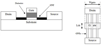
[image:3.612.319.520.462.556.2]CNTs are sheets of Graphene rolled into tubes; depending on the chirality (i.e., the direction in which the grapheme sheet is rolled), a single-walled CNT can be either metallic or semiconducting. Semiconducting nanotubes have attracted widespread attention of device/circuit designers as an alternative possible channel implementation for high-performance transistors. A typical structure of a MOSFET-like CNFET device is illustrated in Figure 5. The CNT channel region is undoped, while the other regions are heavily doped, thus acting as the source/drain extended region and/or interconnects between two adjacent devices. Carbon nanotubes are high-aspect-ratio cylinders of carbon atoms. The electrical properties of a single wall carbon nanotube (SWNT) offer the potential for molecular-scale electronics; a typical semiconducting single-wall carbon nanotube is 1.4nm in diameter with a 0.6eV band-gap (the band-gap is inversely proportional to the diameter). Recent CNFETs have a metal carbide source/drain contact and a top gated structure (Figure 4) with thin gate dielectrics.
Figure 4 CNFET Structure
Two model variants of the CNTFET are provided for analysis from the Stanford University Nanoelectronics Group, one is the Standard CNTFET model and the other is the Uniform tubes CNTFET model. The main difference between them is that the Standard Model takes into account the charge screening effects of the neighboring nanotubes while the Uniform tube Model ignores it. The Standard Model is recommended as it is most accurate and quite fast.
Standard Model. We analyze the characteristics of both NFET and PFET CNTFETs.
Figure 5 CNT-nFET and NMOS Output Characteristics
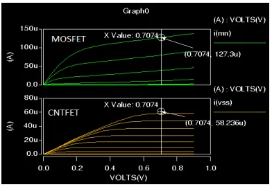
Spice models for CNTFET from Stanford library is read into HSPICE Models Version 2.2.1 and SPICE program to estimate VI characteristics are modeled. The devices are set with number of CNT tubes to 3, chirality single dimension vector to (19, 0) and effective length to 32 nm. The input characteristics
is curve is drawn between the input voltage Vgs and
the output drain current (not shown). The output characteristic curve is drawn between the drain to
source voltage (Vds) and drain current (Idrain) for the
constant different source to gate voltages (Vgs) and
is shown in Figure 5 for CNT-nFET. This characteristic curve gives the pinch-off, linearity and the effect of drain resistance can be observed. The output characteristic shows that the saturation current in CNTFET is more stable than 32 nm MOSFET. The CNTFET is used as a best current source with accuracy in small scale technology. The effect of drain resistance is less in CNTFET as the current becomes of constant, whereas the effect of drain resistance is high in MOSFET and the current is not constant. The current of the CNTFET can be increased by increasing the number of tubes in a CNTFET at room temperature. The leakage power also reduced due to the high stability in saturation current and due to back gate control the SCE is decreased with high performance. The drain current with 3 tubes is 58.236 µA in nFET and
58.37 µA in pFET at Vds=7.024 V. The CNTFET
performance is depending on the chirality, number of tubes and length of the CNT in the CNTFET transistor. The semiconducting CNT purpose and 1-D Quasi CNT chirality is (19, 0) standard representation. For that number of tubes is 3 in effective length of CNT is 32 nm.
Figure 6 shows the I-V characteristics of the ballistic CNTFET with different channel lengths (32nm, 27nm, 21nm, 14nm and 10nm), at
[image:4.612.316.522.151.303.2]the power supply of 0.9V and room temperature. The output I-V characteristics of the CNTFET are similar to that of the MOSFET, which makes the CNTFET a good candidate for current MOSFET based VLSI designs.
Figure 6 I-V Characteristics for Different Length in CNTFET
As shown in Figure 6 the current level of the CNTFET decreases with channel length (when the channel length is very short) due to the energy quantization in the axial direction (as limited by optical phonon scattering). The drain current in 10 nm CNTFET is 25.568 µA and in 32 nm CNTFET 57.775 µA. The current of the CNTFET can be increased by increasing the number of tubes in a CNTFET. For tubes=3 the drain current is 57.775 µA and for tubes=15 the drain current is 286.94 µA. The chirality vector, which is the wrapping vector that the graphite sheet is rolled up along it, is determined by (n1, n2) indices. These indices specify the arrangement angle of the carbon atoms
along the nanotube. If n1−n2! = 3k (k ∈ Z), the
SWCNT is semiconductor and otherwise it is metallic. By changing the n, m dimensions current also changing. By changing the ‘n’ value by 3, 6, 9, 12, 15 the current is increasing and change in ‘m’ by 19, 25, 31, 37, 44 current increasing. The every combination (19, 3), (25, 6).., etc are not equal to multiple of ‘3’ so the CNT is semiconductor in nature. In a CNTFET device one or more semiconducting SWCNTs are used as the channel of the device. Besides the unique properties of the CNT material, removing the channel from the silicon bulk leads to elimination and reduction of
many parasitic elements. For 10% change in Vgs is
reduction are becoming less effective due to the increased impact of static power.
In general, leakage power is different depending on the applied input vector. The average power in CNTFET is less due to high mobility channel between drain and source. The SCE also less due to back gate control present in the CNTFET. The total average power at 0.79544 V is 46.458 µW for CNTFET and for MOSFET is 105.12 µW. The maximum leakage power of the MOSFET-based gates is 75 times larger than for CNTFET gates. The minimum leakage power of the MOSFET is about three times larger than for CNTFET. The maximum leakage power shows a similar trend for both CNTFET and MOSFET based gates, while the minimum leakage power shows somewhat different trends, because the stack effect is reduced in CNTFET circuits.
3.1 Design and Analysis of Inverter
[image:5.612.313.523.333.418.2]For comparing performance at circuit-level, the inverter (as fundamental logic gate) is usually considered first; in this paper, the inverter is designed with minimal width and a number of tubes in 32 nm technology. Logic gates and bench-mark circuits are designed at 32 nm for both CNTFET and CMOS technologies; delay, power, PDP, leakage current and frequency response are simulated and compared.
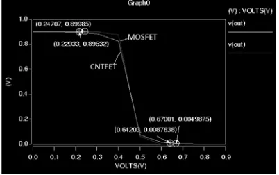
Figure 7 Inverter using CNTFET
Figure 7 shows that the Voltage Transfer Characteristics (VTC) of the CNTFET also has a symmetrical shape at a 1 to 1 (pFET : nFET) ratio. Even though the current in a CNT is smaller than the minimum sized MOSFET (at 32 nm technology), a CNTFET has a steeper curve in the transition region due to the higher gain. This contributes to a 22.5% improvement in Noise Margin (NM), and this progressed performance is preserved under a decrease in power supply voltage. The characteristic curve is sharp in case of CNTFET and hence the static power dissipation is less in the inverter developed using CNTFET. MOSFET and CNTFET can be compared using the PDP as metric. Above comparison shows the delay, power, and PDP of logic gates in 32 nm MOSFET and 32 nm CNTFET technologies; the PDP of the 32 nm MOSFET is about 100 times higher than that of the 32 nm CNTFET.
Table 1 CNTFET Comparison with MOSFET Inverter
Parameters CNTFET MOSFET
Delay 6.0982 ps 15.445 ps
Rise Time 42.086 ps 220.58 ps
Fall Time 37.541 ps 144.05 ps
Average Power 8 µW 20 µW
PDP 48.78 µJoules 308.9 µJoules
3.2 Design And Analysis Of Analog Circuits
One of the basic building blocks of analog circuit design is the Common Source Amplifier. A CSA is an inverting amplifier whose input is connected to the Gate of the transistor and the output is taken at the drain of the transistor. For desired amplification, proper biasing has to be provided to the CSA with the help of current reference realized using current mirror. The current mirrors are designed and analyzed using CNTFET. The maximum current mirroring by nFET is 92.97 µA and pFET is 98.09 µA. Common Source Amplifier (CSA) is designed with pFET based current mirror load. The bias voltage for Class-A mode is VGS=0.7 V and for Class-C bias mode VGS = -0.3 V negative biasing voltage. From the simulation results it was found that the GBW (Gain Band Width) is 125.56 MHz, PM (Phase Margin) is
55.060 and BW (Band Width) is 351.798 MHz.
[image:5.612.89.290.555.681.2]and analysis of differential analog Viterbi decoder using CNTFET.
4. DESIGN OF DAVD USING CNTFETS
Differential analog Viterbi decoder as mentioned consists of Sample/Hold (S/H) Circuit, the decoding is carried out in the current domain hence the voltage to current converter converts the sampled voltages into current equivalents. The branch metric computer unit measure of similarity between the received channel symbols and the trellis branch symbols at each time transition. The add-compare-select unit that operates on parallel data performs online decoding, and the Winner Takes All circuit is the decision making unit that decides the minimum current path. In this work, MOSFETs are replaced using CNTFET in design of all the above sub circuits.
4.1 Sample and hold
Sample and hold circuit [6, 15, 33] is used to interface real-world signals, by changing analogue signals to a subsequent system such as an
[image:6.612.318.522.197.374.2]analog-to-digital converter
.
Figure 8 Sample and Hold Circuit
The purpose of this circuit is to hold the analogue value steady for a short time while the converter or other following system performs some operation that takes a little time. In most circuits, a capacitor is used to store the analogue voltage and an electronic switch or gate is used to alternately connect and disconnect the capacitor from the analogue input. The rate at which this switch is operated is the sampling rate of the system. The decoder designed is rate ½ hence it is required to achieve two samples in one clock cycle. The clock signals that are generated using the clock generator circuit produces two clock signals that are offset by half in one clock period that are used to control the
S/H circuit. The differential input Vin+ and Vin- are
[image:6.612.93.294.395.535.2]applied simultaneously to the S/H circuit. For achieving fast sampling the CNT-nFET source follower is used. The circuit is designed to minimize nonlinearity error and gain error. The sampling capacitors have chosen to have values of 0.1 pF. The S/H circuit shown in Figure 8 has two independent paths that are operated by nonoverlapping clocks.
Figure 9 Branch Metric Unit Schematic
4.2 Voltage To Current Converter
The sampled voltage samples are converted to current samples using the voltage to current converter. The converter circuit designed in [33] using MOSFETs are replaced with CNTFETs. The differential inputs to the circuit biases the
transistors to drive the Iout current across the
CNT-pFET current mirror load at the output. In order to test the circuit functionality two input signals that are sampled are applied at the input terminals, the differential inputs drive the output current, the output current direction changes based on the differential inputs.
4.3 Branch Metric Unit
decoder input signal. Figure 9 shows the modified BMU architecture (MOSFETs replaced with CNTFETs) that is designed to operate based on current samples. The simulation results of BMU show that the current samples are obtained at the required clock samples. The current samples are sent to the add-compare-select unit.
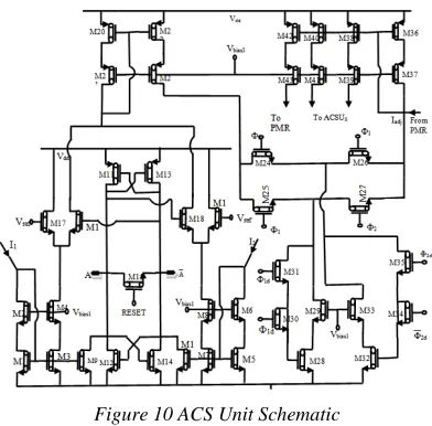
Figure 10 ACS Unit Schematic
4.4 Add-Compare-Select Unit
The add-compare-select (ACS) unit in this circuit is designed to add current samples from the BMC unit thus eliminate the use of adder unit. In addition, the use of CNTFETs for circuit design resulted in faster and less power dissipation. Unlike previous digital ACS designs, the proposed approach uses current mode techniques, and since no digital logic functional blocks are required. General implementation of unit adder requires 36 transistors. The modified design implements the same logic using only 24 transistors. The ACSU functional block diagram and simulation results are shown in Figure 10.
4.5 Winner-Take-All (WTA)
[image:7.612.96.292.179.372.2]The WTA architecture (shown in Figure 11) consists of six 2-input RCC circuits that are identified as three clocks and the outputs of each block is connected to the latch [6, 33].
Figure 11 Winner Take All Circuit using CNTFETs
The WTA architecture is arranged as tree structure and the clock signals are generated to sequentially control the modules. The upper ACS and the lower ACS outputs are applied to the four pairs of RCC unit, the outputs of RCC are further process by the second level of RCC unit and finally only a binary output decision as to where the path with the smallest metric originates from is necessary in the last stage of the WTA block. Thus, a simple CNTFET latch can be used to establish this. The CNTFET latch consists of two back-to-back inverters and a reset switch. The WTA circuit is a structure compared with [34] as redundant current replications are eliminated reducing power dissipation and complexity; also the CNTFET used drive more current and hence reduces delay.
4.6 Replicating Current Comparator (RCC) Circuit
Figure 15 NCNTFET RCC Unit Schematic
The clock generator circuit generates non-overlapping clock signals and the bias circuit as discussed in [33] is designed using CNTFETs. The biasing circuit generates necessary biasing voltages, biasing circuitry is included to provide on-chip biasing generated from the power supply. The four bias voltages are set by the external reference current source. The biasing circuit takes input current of 200µA with voltage reference Vref of 0.65mV generates different biases of Vbias3, Vbias2 and Vbias1 of 1.05V, 1.2V and 1.4V respectively. These biasing voltages are required for add-compare-select circuit and branch metric unit and also clock generator circuit utilizes.
5. RESULTS AND DISCUSSION
The differential analog Viterbi decoder designed using CNTFETs are modeled using Spice Code and is simulated using Hspice. The individual sub blocks are modeled as sub circuits are integrated to model the top level model of differential analog Viterbi decoder. The model files for CNTFET are downloaded from Stanford Nanoelectronics Centre under permission and are
used for simulation. The transistor geometries are
designed for optimum drive strength and maximum frequency of operation.
The S/H operates at a clock period of 2ns and hold the data for duration of 20ns. The power consumption is about 0.096 mW and the maximum frequency of operation is 480 MHz with a load capacitance of 100pF. The S/H circuit is verified for an input signal with frequency of 200 KHz, sampled at 480Msamples per second.
Voltage to converter is designed using CNTFETs with geometries Wp/Wn (0.5µ/150n). The transistor geometries are set to the size of S/H
circuit. The V2I is simulated for duration of 6 clock cycles (T-count). The input voltage applied to V2I from the S/H circuit is converted to current of maximum of 45 µA.
The ACSU receives two outputs generated from BMU which are given to differential ACSU
logic. Input signals Vrm and Vrp are applied at two
different carrier frequency of 100KHz and 200KHz, the input signals are processed to two sets of current output samples and are fed into the ACSU. The bias voltage is set to 100mV.
The delay of the BMU unit is 11.2 ns. The maximum operating frequency of BMU is 562 MHz. Power dissipation is found to be 132µW which is less than 2.5 than [33]. In the differential decoder logic, two ACSU operate in parallel, the transistor geometries are chosen for optimum performance.
[image:8.612.91.298.73.251.2]The maximum operating frequency of ACSU is 478 MHz and power consumption is less than 210µW. The Winner Take All circuit needs to operate for 92 clock cycles and the minimum and maximum current are set to 1µA and 5µA respectively. The clock generator, RCC and biasing circuit are designed and simulated for its functionality. The transistor geometries are designed for optimum performance. The nonlinearities of analog circuit designed are compensated based on matching circuits, the width of NCNTFET and PCNTFET are identified for symmetric layout design. The results obtained are compared with the reference designs and are reported for comparison. Table 2 compares the performances of the CNTFET based DAVD with analog Viterbi decoder design.
Table 2 Comparison of DAVD with AVD
Parameters This Work
DAVD [33]
AVD [15]
Technology 32nm CNTFET
0.13 µm CMOS
0.8 µm CMOS Supply voltage 1.0 V 1.2 V 2.8 V Core area (mm2) 0.0912 0.2 1
Maximum speed (Mbps)
500 200 115
Power dissipati on (µW)
Desired 500 1.2 14.9 BMC 132 340 1.9 ACSU 210 800 9.4 Bias
circuit
97 207 2.5
due to change in technology and power supply voltage, but the optimization carried out in the design of circuit schematic. In order to optimize the layout for its area, layout techniques such as common centroid and inter-digitization methods are adopted. Optimum choice of drivers and sizing of drivers will improve the driving capability of sub systems. Transistor sizing and ordering of transistors will minimize the delay in sub systems.
6. CONCLUSION
Analog Viterbi decoders are realized using differential decoder logic. In this work, two different ACSU is sued to decode the encoded message signal. The output of S/H circuit is voltage which is converted to current samples and is used in decoding. Thus the proposed design reduces the number of transistors and also improves the operating frequency. The proposed design is verified for its functionality based on Matlab models for various test vectors. The transistor geometries are designed for optimum performance and is captured using Hspice. The differential analog Viterbi decoder implemented using 32 nm CNTFET transistors. The soft decision Viterbi decoder achieves 65% improvement as compared to hard decision Viterbi decoder and the BER performance also better than conventional Viterbi decoder. Sample and hold unit is implemented and is utilizing 96 µW of power, voltage to current
converter draws 45 µA, and branch metric
computation unit is implemented as a sub block of Viterbi decoder 132 µW of power. Add-Compare-Select Unit is implemented and is utilizing 4.14nA of current. The designed DAVD is suitable for low power and high speed applications. The circuit performance can be further enhancing with impedance matching circuits at the output of BMU and ACSU.
ACKNOWLEDGEMENT:
The authors would like to acknowledge the support and suggestions provided by Dr. Cyril Prasanna Raj P., Chaitanya, Krishnaveni and Priya Maheshwari and MSRSAS in carrying out this work. The authors would like to thank Dr. NJR Muniraj (Teja Shakthi College of Engineering, Coimbatore) for suggestions provided in carrying out this work. The authors would like to acknowledge Stanford Nanotechnology Centre for the access provided in using the CNTFET model files.
REFERENCES:
[1]. Jia L.; Gao Y.; Isoaho J.,;Tenhunen H.: Design
of a super-pipelined Viterbi decoder, Proc.
ISCAS’99, Orlando, FL, vol. 1, 1999, pp. 133–
136
[2]. Sridharan S.; Carley L. R.: A 100-MHz
350-mW 0.6-µm CMOS 16-state generalized-target
Viterbi detector for disk drive read channels.
IEEE J. Solid-State Circuits, vol. 35, no. 3,
2000, pp. 362–370
[3]. Matthews T. W. ; Spenser R. R.: An integrated
analog Viterbi detector for digital magnetic
recording. IEEE J. Solid-State Circuits, vol. 28,
no. 12, 1993, pp. 1294–1302
[4]. Shakiba M. H.; Johns D. A.; Martin K. W.:
BiCMOS circuits for analog Viterbi decoders.
IEEE Trans. Circuits Syst. II, Analog Digital
Signal Process., vol. 45, no. 12, 1998, pp.
1527–1537
[5]. He K.; Cauwenberghs G.: Integrated 64-state
parallel analog Viterbi decoder. Proc.
ISCAS’00, Geneva, Switzerland, vol. IV, 2000, pp. 761–764
[6]. Demosthenous A.; Taylor J.: A 100-Mb/s
2.8-V CMOS current mode analog 2.8-Viterbi decoder.
IEEE J. Solid-State Circuits, vol. 37, no. 7,
2002, pp. 904–910
[7]. Zand B.; Johns D. A.: High-speed CMOS
analog Viterbi detector for 4-PAM
partial-response signaling. IEEE J. Solid-State
Circuits, vol. 37, no. 7, 2002, pp. 895–903
[8]. Kim H.; Son H.; Roska T.; Chua L. O.:
High-performance Viterbi decoder with circularly
connected 2-DCNN unilateral cell array. IEEE
Trans. Circuits Syst. I: Regular Papers, vol.
52, no. 10, 2005, pp. 2208–2218
[9]. Lustenberger F.; Helfenstein M.; Moschytz G.
S.; Loeliger H. -A.; Tarkoy F.: All–analog decoder for a binary (18, 9, 5) tail–biting trellis
code. Proc. ESSIRC’99, Duisburg, Germany,
Sep. 1999, pp. 362–365
[10]. Moerz M.; Gabara T.; Yan R.; Hagenauer
J.: An analog 0.25 um BiCMOS tail biting
MAP decoder. Proc. IEEE Int. Solid-State
Circuits Conf. (ISSCC’00), San Francisco, CA, 2000, pp. 356–357
[11]. Winstead C.; Jie D.; Shuhuan Y.; Myers
C.; Harrison R. R.; Schlegel C.: CMOS analog
MAP decoder for (8,4) Hamming code. IEEE
J. Solid-State Circuits, vol. 39, no. 1, 2004, pp. 122–131
[12]. Winstead C.; Nguyen N.; Gaudet V. C.;
Schlegel C.: Low-voltage CMOS circuits for
Syst. I: Regular Papers, vol. 53, no. 4, 2006, pp. 829–841
[13]. Hemati S.; Banihashemi A. H.; and Plett
C.: A 0.18-umCMOS analog min-sum iterative decoder for a (32,8) low-density parity-check
(LDPC) code. IEEE J. Solid-State Circuits,
vol. 41, no. 11, 2006, pp. 2531–2540
[14]. Howard S. L.; Schlegel C.; Iniewski K.:
Error control coding in low-power wireless sensor networks: When is ECC
energy-efficient. EURASIP J. Wireless Commun.
Netw., vol. 2006, 2006, p. 1-14
[15]. Demosthenous A.; Taylor J.: A 100-Mb/s
2.8-V CMOS current mode analog Viterbi
decoder. IEEE J. Solid-State Circuits, vol. 37,
no. 7, 2002, pp. 904–910
[16]. Shakiba M. H.; Johns D. A.; Martin K. W.:
An integrated 200-MHz 3.3- V BiCMOS class-IV partial response analog Viterbi decoder.
IEEE J. Solid-State Circuits, vol. 33, no. 1,
1998, pp. 61–75
[17]. He K.; Cauwenberghs G.: An integrated
64-state parallel analog Viterbi decoder. Proc.
ISCAS, 2000, pp. IV.761–IV.764
[18]. Acampora A.; Gilmore R.: Analog Viterbi
Decoding for High Speed Digital Satellite
Channels. IEEE Transactions on
Communications, vol. 26, no. 10, 1978, pp.
1463-1470
[19]. Demosthenous A.; Taylor J.: Effects of
signal-dependant errors on the performance of
switched-current Viterbi decoders. IEEE
Transactions on Circuits and Systems I: Fundamental Theory and Applications, vol. 48, no. 10, 2001, pp. 1225–1228
[20]. Wen-Ta Lee; Ming-Jlun; Yuh-Shyan
Hwang; Jiann-Jong Chen, “IC Design of a New Decision Device for Analog Viterbi
Decoder”, Institute of Computer and
Communication, National Taipei University of
Technology Taipei, Taiwan, R.O.C. (2006)
Online:
http://140.117.166.1/eehome/ISCOM2005/Sub mitPaper/UploadPapers/ISCON05_00133.pdf
[21]. Janne Maunu; Mika Laiho; Ari Paasio. A
Differential Architecture for an Online Analog Viterbi Decoder. IEEE Trans. On Circuits and Systems—I, Vol. 55, No. 4, 2008, pp. 1133-1140
[22]. J. Appenzeller: Carbon nanotubes for
high-performance electronics—Progress and
prospect. Proc. IEEE, vol. 96, no. 2, 2008, pp.
201–211
[23]. A. Rahman; J. Guo; S. Datta; M. S.
Lundstrom: Theory of ballistic nano
transistors. IEEE Trans. Electron Device, vol.
50, no. 10, 2003, pp. 1853–1864
[24]. A. Akturk; G. Pennington; N. Goldsman;
A. Wickenden: Electron transport and velocity
oscillations in a carbon nanotube. IEEE Trans.
Nanotechnology., vol. 6, no. 4, 2007, pp. 469– 474
[25]. H. Hashempour; F. Lombardi: Device
model for ballistic CNFETs using the first
conducting band. IEEE Des. Test. Comput.,
vol. 25, no. 2, 2008, pp. 178–186
[26]. Y. Lin; J. Appenzeller; J. Knoch; P.
Avouris: High-performance carbon nanotube field-effect transistor with tunable polarities.
IEEE Trans. Nanotechnology., vol. 4, no. 5,
2005, pp. 481–489
[27]. Sheng Lin, Yong-Bin Kim and Fabrizio
Lombardi, CNTFET-Based Design of Ternary
Logic Gates and Arithmetic Circuits, IEEE
Trans. On Nanotechnology, Vol. 10, No. 2,
2011, pp: 217-225
[28]. Stanford University CNFET model
Website: Stanford University, Stanford, CA [Online].
http://nano.stanford.edu/model.php?id=2,
accessed on 10th March 2012
[29]. Deng J.; Wong H.-S. P.: A compact
SPICE model for carbon-nanotube field-effect
transistors including nonidealities and its application—Part I: Model of the intrinsic
channel region. IEEE Trans. Electron Device,
vol. 54, no. 12, 2007, pp. 3186–3194
[30]. Deng J.; Wong H.-S. P.: A compact
SPICE model for carbon-nanotube field-effect
transistors including nonidealities and its application—Part II: Full device model and
circuit performance benchmarking. IEEE
Trans. Electron Device, vol. 54, no. 12, 2007, pp. 3195–3205
![Figure 2 Block Diagram of Decoder [6]](https://thumb-us.123doks.com/thumbv2/123dok_us/8914540.961094/2.612.100.282.494.638/figure-block-diagram-of-decoder.webp)