Performance Analysis of Floating Point Adder using
VHDL on Reconfigurable Hardware
Karan Gumber
University institute of engineering and technology Panjab University, Chandigarh
India
Sharmelee Thangjam
University institute of engineering and technology Panjab University, Chandigarh
India
ABSTRACT
Floating point addition is more difficult than multiplication because alignment of mantissa is required before mantissa addition. The main objective of implementation of floating point adder on reconfigurable hardware i.e. on Virtex is to utilize less chip area with less combinational delay and faster speed. Less combinational delay means less latency i.e. less time is required to appear an output after the input response is applied and if there is less latency then there will be the faster speed and lesser the clock period. Implementation of floating point adder on Virtex 4 produces a least combinational delay of 24.201nsec consuming 4% of chip area while implementing same on Spartan 2 produces the greatest combinational delay of 79.594nsec consuming 92% of chip area. Less chip area means less number of slices is used in reconfigurable hardware i.e. on FPGAs.
General Terms
Clock speed, Combinational delay, Chip area, Clock period, Algorithms
Keywords
Floating point addition, FPGAs, VHDL, Xilinx
1.
INTRODUCTION
Floating point operations are hard to implement on reconfigurable hardware i.e. on FPGAs because of their complexity of their algorithms. On the other hand, many scientific problems require floating point arithmetic with high level of accuracy in their calculations. Therefore VHDL programming for IEEE single precision floating point adder in have been explored. For implementation of floating point adder on FPGAs module various parameters i.e. clock period, latency, area (number of slices used), total number of paths/ destination ports, combinational delay, modeling formats etc will be outline in the synthesis report. VHDL code for floating point adder is written in Xilinx 8.1i and its synthesis report is shown in Design process of Xilinx which will outline various parameters like number of slices used, number of slice flip flop used, number of 4 input LUTs, number of bonded IOBs, number of global CLKs. Floating point addition is most widely used operation in DSP/Math processors, Robots, Air traffic controller, Digital computers because of its raising application the main emphasis is on the implementation of floating point adder effectively such that it uses less chip area with more clock speed[1][2].
2.
FLOATING POINT FORMAT
The advantage of floating point over fixed point format is the range of numbers that can be presented with the fixed number of bits. Floating point number is composed of three fields and
can be of 16, 18, 32 and 64 bit. Figure shows the IEEE
standard for floating point numbers [3] [4].
31 30 22 0
1 bit sign of signifies whether the number is positive or negative. „1‟ indicates negative number and „0‟ indicate positive number. 8 bit exponent provides the exponent range from E (min) =-126 to E (max) =127. 23 bit mantissa signifies the fractional part of a number the mantissa must not be confused with the significand. The leading „1‟ in the significand is made implicit [3].
2.1 Conversion of Decimal to Floating
numbers
Conversion of Decimal to Floating point 32 bit format is explained with example. Let us take an example of a decimal number that how could it will be converted into floating format. Enter a decimal number suppose 129.85 before converting into floating format this number is converted into binary value which is 10000001.110111. After conversion move the radix point to the left such that there will be only one bit which is left of the radix point and this bit must be 1 this bit is known as hidden bit and also made above number of 24 bit including hidden bit which is always „1‟ like 1.00000011101110000000000 the number which is after the radix point is called mantissa which is of 23 bits and the whole number is called significand which is of 24 bits. Count the number of times the radix point is shifted say „x‟. But in above case there is 7 times shifting of radix point to the left. This value must be added to 127 to get the exponent value i.e. original exponent value is 127 + „x‟. In above case exponent is 127 + 7 = 134 which is 10000110. Sign bit i.e. MSB is „0‟ because number is +ve. Now assemble result into 32 bit format which is sign, exponent, mantissa. 01000011000000011101110000000000. Now take another example which is totally different from above let us enter a decimal number -0.5 which is converted into binary value which is .000011. After conversion move the radix point to the right in this case such that there will be only one bit which is left of the radix point and this bit must be 1 this bit is known as hidden bit and also made above number of 24 bit including hidden bit which is always „1‟ 1.10000000000000000000000 the number which is after the radix point is called mantissa which is of 23 bits and the whole number is called significand which is of 24 bits. Count the number of times the radix point is shifted to the right say „x‟. In this case there is 5 times shifting of radix point to the right. This value must be subtracted to 127 to get the exponent value i.e. original exponent value is 127 - „x‟. In above case
exponent is 127 - 5= 122 which is 01111010. Sign bit i.e. MSB is „1‟ because number is -ve. Now assemble result into 32 bit format which is sign, exponent, mantissa 10111101010000000000000000000000.
#Note: - Hidden bit is not included into 32 bit format this bit is implicit. When performing operation with this format this implicit bit is made explicit [4] [5]
3.
ADDITION ALGORITHM FOR
FLOATING POINT NUMBERS
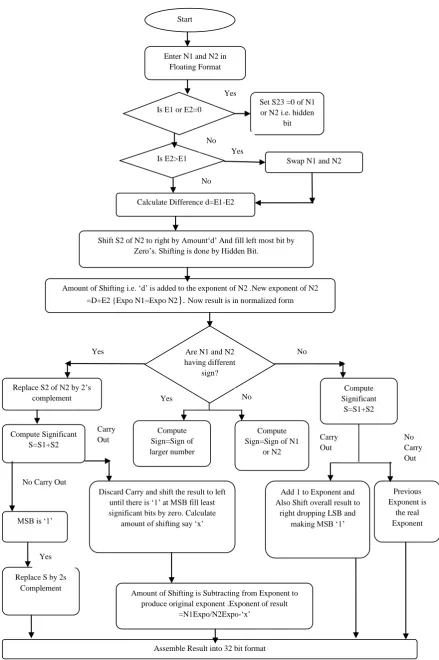
The floating point addition is the most complex operation then the floating point multiplication since the alignment of mantissa is required before mantissa addition. I would like to explain floating point addition algorithm in 2 cases with example. Case I is when both the numbers are of same sign i.e. when both the numbers are either +ve or –ve means the MSB of both the numbers are either 1 or 0. Case II when both the numbers are of different sign i.e. when one number is +ve and other number is –ve means the MSB of one number is 1 and other is 0. The flowchart of the algorithm is given below in next page and it is explained in following steps with proper example.
3.1
Case I: - When both numbers are of
same sign
Step 1:- Enter two numbers N1 and N2. E1, S1 and E1, S2 represent exponent and significand of N1 and N2.
Step 2:- Is E1 or E2 =‟0‟. If yes set hidden bit of N1 or N2 is zero. If not then check is E2 > E1 if yes swap N1 and N2 now contents of N2 in N1 and N1 in N2 and if E1 > E2 make contents of N1 and N2 same there is no need to swap.
Step 3:- Calculate difference in exponents d=E1-E2. If d = „0‟ then there is no need of shifting the significand and if d is more than „0‟ say „y‟ then shift S2 to the right by an amount „y‟ and fill the left most bits by zero. Shifting is done with hidden bit.
Step 4:- Amount of shifting i.e. „y‟ is added to exponent of N2 value. New exponent value of E2= previous E2 + „y‟. Now result is in normalize form because E1 = E2.
Step 5:- Is N1 and N2 have different sign „no‟. In this case N1 and N2 have same sign.
Step 6:- Add the significands of 24 bits each including hidden bit S=S1+S2.
Step 7:- Is there is carry out in significand addition. If yes then add „1‟ to the exponent value of either E1 or new E2 and shift the overall result of significand addition to the right by one by making MSB of S is „1‟ and dropping LSB of significand.
Step 8:- If there is no carry out in step 6 then previous exponent is the real exponent.
Step 9:- Sign of the result i.e. MSB = MSB of either N1 or N2.
Step 10:- Assemble result into 32 bit format excluding 24th bit
of significand i.e. hidden bit [6] [7]. Example Step 1: Enter N1 and N2.
N1=2.3=0 10000000 100100100000000000000000 N2=7.4=0 10000001 111011000000000000000000 E1= 10000000
E2= 10000001
S1=100100100000000000000000 S2= 111011000000000000000000 Step 2: If E2>E1. Yes then swap N1 & N2.
New N1=0 10000010 111011000000000000000000 New N2=0 10000000 100100100000000000000000 Step 3: Calculate d =E1-E2.
10000001-10000000 = 1
Step 4: Shifting of S2 to the right by one and also add 1 to E2. N2 =0 10000000 100100100000000000000000(original) N2= 0 10000000 010010010000000000000000 (one time shifted)
Shifting by 1 time means add „1‟ to exponent.
Step 5: New exponent value E2 = 10000001, new significand value S2 = 010010010000000000000000 here E1 = E2. Step 6: S=S1+S2.
S1=111011000000000000000000 S2=010010010000000000000000
S=1001101010000000000000000
Step 7: Here is carry out add „1‟ to exponent and shift result to the right by one bit and discard the LSB of „S‟.
Original exponent=10000010
Original significand=100110101000000000000000 Step 8: MSB of result is „0‟.
Step 9: Assemble into 32 bit format. 0 10000010 00110101000000000000000
3.2
Case II: - When both numbers are of
different sign
Step 1, 2, 3 & 4 are same as done in case I. Step 5:- Is N1 and N2 have different sign „Yes‟.
Step 6:- Take 2‟s complement of S2 and then add it to S1 i.e. S=S1+2‟s complement of S2.
Step 7:- Is there is carry out in significand addition. If yes then discard the carry and also shift the result to left until there is „1‟ in MSB also counts the amount of shifting say „z‟. Step 8:- Subtract „z‟ from exponent value either from E1 or E2. Now the original exponent is E1-„z‟. Also append the „z‟ amount of zeros at LSB.
Step 9:- If there is no carry out in step 6 then MSB must be „1‟ and in this case simply replace „S‟ by 2‟s complement. Step 10:- Sign of the result i.e. MSB = Sign of the larger number either MSB of N1or it can be MSB of N2.
Step 10:- Assemble result into 32 bit format excluding 24th bit
of significand i.e. hidden bit [8][9]. Example
Step 1: Enter N1 and N2.
N1=128.5=0 10000110 100000001000000000000000 N2=-18.25=1 10000011 100100100000000000000000 E1=10000110
E2=10000011
S1=100000001000000000000000 S2=100100100000000000000000 Step 2: E1>E2 no need to swap. Step 3: Calculate„d‟=E1-E2
10000110-10000011=00000011=>3 in decimal.
Step 4: Shifting of S2 to the right by three and also add 3 to E2.
Figure 1: Algorithm for floating point addition Start
Enter N1 and N2 in Floating Format
Is E1 or E2=0
Is E2>E1
Calculate Difference d=E1-E2
Set S23 =0 of N1 or N2 i.e. hidden
bit
Swap N1 and N2
Shift S2 of N2 to right by Amount„d‟ And fill left most bit by Zero‟s. Shifting is done by Hidden Bit.
Amount of Shifting i.e. „d‟ is added to the exponent of N2 .New exponent of N2 =D+E2 {Expo N1=Expo N2}. Now result is in normalized form
Are N1 and N2 having different
sign?
Discard Carry and shift the result to left until there is „1‟ at MSB fill least significant bits by zero. Calculate
amount of shifting say „x‟
Compute Sign=Sign of N1
or N2
Compute Significant
S=S1+S2
Add 1 to Exponent and Also Shift overall result to
right dropping LSB and making MSB „1‟
Previous Exponent is
the real Exponent Replace S2 of N2 by 2‟s
complement
Compute Significant S=S1+S2
Amount of Shifting is Subtracting from Exponent to produce original exponent .Exponent of result
=N1Expo/N2Expo-„x‟
Assemble Result into 32 bit format Replace S by 2s
Complement
Compute Sign=Sign of larger number
MSB is „1‟
Yes
yes
No Yes
No
No Yes
Yes No
No Carry Out Carry
Out Carry
Out
N2 = 0 10000100 010010010000000000000000 (1 time shifting)
N2 = 0 10000101 001001001000000000000000 (2 time shifting)
N2 = 0 10000110 000100100100000000000000 (3 time shifting)
Shifting by 1 time means add „1‟ to exponent.
Step 5: New exponent value E1 = 10000110, new significand value S2 = 000100100100000000000000 here E1=E2 i.e. result is in normalized form.
Step 6: Take 2‟s complement of S2 because S2 is -ve i.e. S=S1+2‟s complement of S2.
S1=100000001000000000000000 S2=111011011100000000000000
S=1011011100100000000000000
Step 7: Here is carry out add lets discard the carry and shift result to the left by one bit to make MSB „1‟ and then subtract the amount of shifting from E1 or E2 to form original exponent of result.
Original exponent=10000110-1=10000101 Original significand=110111001000000000000000
Step 8:- Sign bit of result i.e. MSB= Sign of 128.5 which is larger number.
Step 9: Assemble into 32 bit format.
0 10000101 110111001000000000000000
3.3
Special Conditions
There are some special conditions while implementing floating point adder which needs to be handle these are explained below
1: If N1 = N2 = „0‟ then overall result is „0‟.
2: If E1=E2 and sign bit of E1 ≠ E2 then again overall result is „0‟.
3: If E1= „0‟ and E2 ≠ „0‟ then overall result is equal to E2. 4: If E2= „0‟ and E1 ≠ „0‟ then overall result is equal to E1 5: If d= E1-E2 ≥24 then overall result is larger of E1 or E2 [10].
3.4
Problems associated in addition
There are two problems which occurs when we are going to add two floating point numbers
1: When the exponent of two numbers are different this can be solved by shifting the significand of smaller number to the right by an amount equal to exponent difference and this amount is added to exponent value of smaller number to make exponent of both the numbers are same means in normalized form
2: When there is carry out in significand addition if both the number are of different sign then add „1‟ to the exponent and shift the result of significand to the right by one discarding LSB and if both the number are of different sign then discard the carry and shift the result to the left until there is „1‟ at MSB the amount of shifting is subtracted from exponent to form real exponent [10] [11].
4.
SYNTHESIS REPORT
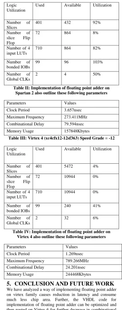
These are the final results which are obtained in the synthesis report when we are going to simulate VHDL code of floating point adder on Spartan 2 and Virtex 4.Table I and Table II show the implementation of floating point adder on Spartan 2. .Table III and Table IV shows the implementation of floating point adder on Virtex 4. The parameters such as number of
slices, number of slice flip flop, GCLKs are outline in the synthesis report are as follows.
Table I: Spartan 2(xc2s30-6tq144) Speed Grade = -6
Logic Utilization
Used Available Utilization
Number of Slices
401 432 92%
Number of slice Flip Flop
72 864 8%
Number of 4 input LUTs
710 864 82%
Number of bonded IOBs
99 96 103%
Number of Global CLKs
[image:4.595.302.553.123.759.2]2 4 50%
Table II: Implementation of floating point adder on Spartan 2 also outline these following parameters
Parameters Values
Clock Period 3.657nsec
Maximum Frequency 273.411MHz
Combinational Delay 79.594nsec
Memory Usage 157848Kbytes
Table III: Virtex 4 (xc4cfx12-12sf363) Speed Grade = -12
Logic Utilization
Used Available Utilization
Number of Slices
401 5472 4%
Number of slice Flip Flop
72 10944 0%
Number of 4 input LUTs
710 10944 0%
Number of bonded IOBs
99 240 41%
Number of Global CLKs
2 32 6%
Table IV: Implementation of floating point adder on Virtex 4 also outline these following parameters
Parameters Values
Clock Period 1.269nsec
Maximum Frequency 789.266MHz
Combinational Delay 24.201nsec
Memory Usage 244468Kbytes
5.
CONCLUSION AND FUTURE WORK
delay and less consumption of chip area. In future, these modules can be converted to IEEE-754 double-precision format. The implementation of these units will ease the implementation of computationally intense scientific applications.
6.
ACKNOWLEDGMENTS
I would like to thanks the anonymous reviewers for their insightful comments.
7.
REFERENCES
[1] Ali malik, Dongdong chenand Soek bum ko, “Design
tradeoff analysis of floating point adders in FPGAs,” Can. J. elect. Comput. Eng., ©2008IEEE.
[2] Loucas Louca, Todd A cook and William H. Johnson, “Implementation of IEEE single precision floating point addition and multiplication on FPGAs,”©1996 IEEE.
[3] Alexandru, Mircea, Lucian and Oana, “Exploiting parallelism in double path adder structure for increase througput of floating point addition ,” ©2007 IEEE.
[4] V. Y. Gorshtein, A. I Grushin, SR Shevtsov, “Floating point addtion method and apparatus,” Sun microsystem U.S patent 5808926,1998.
[5] IEEE std. 1076-2002, “IEEE stsndard VHDL reference manual,” Sponsored by Design Automation standards Committee published by IEEE.
[6] Metin Mete, Mustafa Gok, “A multiprecision floating
point adder,” ©2011 IEEE.
[7] Florent de Dinechin, “Pipelined FPGA adders,” ©2010
IEEE.
[8] Ali malik, Soek bum ko , “Effective implementation of
floating point adder using pipelined LOP in FPGAss,” ©2010 IEEE.
[9] Allan, Wayne Luk, “ Parametised floating point
arithmetic on FPGA,”© 2001 IEEE.
[10] Dr. John A. Eldon, Craig Robertson, “ A floating point format for signal processing,” ©2002 IEEE.