© 2016, IRJET | Impact Factor value: 4.45 | ISO 9001:2008 Certified Journal | Page 272
Realization of a high speed RF data acquisition system
Yashaswini DJ
1, Muniraju
2, Nayana DK
3PG Student, Mtech in VLSI Design and Embedded systems, REVA ITM Bangalore- 560064
1Design Engineer - Centum Electronics Limited,Bangalore
2Asst. Prof. , (ECE), REVA ITM,Bangalore
3
Abstract
—This is an era of ELECTRONIC WARFARE.The modern technologies used to exploit the
Electromagnetic Spectrum are remarkable. Hence this paper presents the design and implementation of a high speed RF Data acquisition system which will characterize an RF signal by extracting the primitive parameters like Frequency and Phase. Characterization of RF signals is very important in ELINT systems as the parameters of the RF signal through a RADAR will help in determining the exact location and source of the RADAR. The Data Acquisition System is a part of the QDR (Quad Digital Receiver). The algorithms of the sub modules which constitute the Data Acquisition System are implemented in VHDL. The synthesis and simulation results have also been presented.
Key words—Electronic warfare; Quad Digital
Receiver; Data Acquisition; RF Data;
1.I
NTRODUCTIONIn Electronic Warfare it is very essential to accurately determine the radar's intrapulse parameters in real time, so that the radar signal can be characterized accurately. This characterization plays a very important role as it aids in estimating the possible counter action against the intended radar. Primary focus would be to determine the fundamental parameters like frequency, amplitude, direction and time of arrival and pulse width of the radar signals. Though Analog receivers have the capability to measure the fundamental parameters they have a limitation towards sensitivity and accuracy. Hence digital receivers have made a fine mark in such systems by overcoming the limitations.
2.O
VERVIEWQDR
SYSTEM2.1
Description
The Quad Digital Receiver (QDR) is an important sub-system of the satellite based ELINT payload for determining intrapulse parameters such as instantaneous
frequency, amplitude, direction of arrival, pulse width of the radar signals in real time.
2.2
Functionality of a QDR system
It detects the video threshold in order to aid data acquisition. It also measures the signal frequency using Digital Instantaneous Frequency Measurement (DIFM) technique. It aids in measuring various parameters such as amplitude, pulse width using the analogue video signal. It computes the angle of arrival (AOA) using the Base Line Interferometry technique by simultaneously sampling the four IF signals corresponding to four antenna elements of the Azimuth/Elevation array.
2.3
Operation
The QDR accepts an IF channel in the frequency range of 1000 ± 250 MHz/ 160 ± 20 MHz for Instantaneous Frequency Measurement and two Video channels for signal detection/threshold and pulse parameters estimation are also available at the input of QDR.
It also accepts 4 channels for direction finding applications. The IF signals are amplified in signal conditioning circuits and passed through 3dB Hybrid to generate I and Q signals, which are digitized using high speed ADC’s. The logic in FPGA receives the digitized signals with which it determines phase, frequency and angle of arrival of the signal. The video channel is used to generate the data valid trigger and this enables the measurement of pulse width. The output from the receiver is packetized as PDW (Pulse Description Word) and transmitted to data handling system.
3.D
ATAA
CQUISITIONS
YSTEM© 2016, IRJET | Impact Factor value: 4.45 | ISO 9001:2008 Certified Journal | Page 273 signal conditioning circuit and then through high speed
ADCs ( Analog-to-Digital converter) and then the signal is given to the logic in the FPGA. In addition to that two video channels are given for threshold detection
3.1
System Description
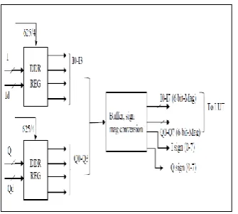
Fig. 1.Data Acquisition system showing the inputs and outputs
[image:2.595.52.268.165.404.2] [image:2.595.52.220.573.723.2]The output is the phase and frequency. With some additional circuitry and logic, it is also possible to determine the amplitude and pulse width. An external LUT (Look Up Table) is present in order to calculate the frequency with the help of the phase obtained as an output from FPGA.
Fig. 2.Process flow of the Data Acquisition System
3.2
Basic Operation
Fig. 2. represents the process flow of the system.The first step is data acquisition in the DDR register. The instantaneous frequency measurement is carried out in this FPGA by using DDIFM technique.
Once the data is obtained, it is given as read address to the LUT. Look up tables are constructed using the block RAMs. From the available data, phase computation is done and the phases are pipelined into 128 phases. 128 samples are acquired and processed for getting the frequency update. Threshold is generated by an external high speed comparator. The reference for the comparator is generated by DAC whose input is programmable within FPGA. The FPGA is connected to the controller via SPI bus. The processor at power ON initializes the phase angle LUT and external LUT for frequency measurement. Data I and Q (MSB 6+1 bits) is acquired in DDR mode by FPGA-1 at 625/4 MHz The 8 samples of I and Q are arranged as a block, for processing. The most likely phase is obtained through normalization and then the frequency is computed using the external Look up table.
The modal filtering concept is used for removing the invalid samples for getting better estimate of the frequency.
Data I and Q (MSB 6+1 bits) is acquired in DDR mode by FPGA-1 at 625/4 MHz The 8 samples of I and Q are arranged as a block, for processing.
3.3
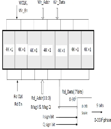
LUT Configuration
© 2016, IRJET | Impact Factor value: 4.45 | ISO 9001:2008 Certified Journal | Page 274
Fig. 3.BRAM configuration
3.4
Modal filter and Phase measurement
Fig. 4.Phase Measurement
The difference between adjacent phases will be computed with added delay of 2π. These difference phases will be sorted into 16 groups and the group with the maximum concentration will be used. The mean value of the phase in the most concentrated group is assumed as best estimation. 3 such filtering will be employed to get difference phases ɸT,ɸ4Ts and ɸ16Ts. These phases are
input to the ambiguity resolving logic module and the module outputs the unwrapped phase ɸ16Ts.
3.5
Phase to Frequency
The unwrapped phase output ɸ16Ts addresses the external memory LUT where frequency values are stored. One Frequency output is generated for every 128 input samples which is used for phase correction and direction finding in other FPGAs.
4.S
YNTHESIS AND SIMULATION RESULTS4.1 Data acquisition through DDR
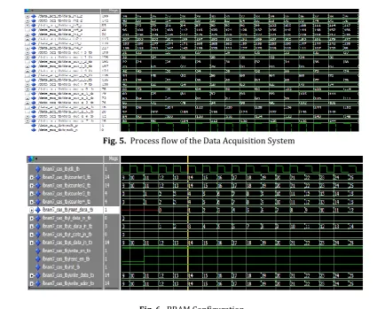
Fig. 3. shows the data acquisition result through the DDR. The data passed through four DDR registers will result in 8 data. Hence four component of I and Q data each gives a total of sixteen output data lines.
4.2 BRAM Configuration
© 2016, IRJET | Impact Factor value: 4.45 | ISO 9001:2008 Certified Journal | Page 275
Fig. 5. Process flow of the Data Acquisition System
Fig. 6. BRAM Configuration
.
[image:4.595.81.507.85.434.2]
© 2016, IRJET | Impact Factor value: 4.45 | ISO 9001:2008 Certified Journal | Page 276
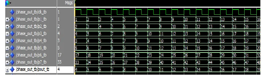
Fig. 8. Phase output
5.C
ONCLUSIONDifferent algorithms were implemented and the most optimized one was selected for the design. Optimization parameters considered were in terms of speed and resource utilization. Following the entire process flow, each sub module as designed as per the demanded specifications and the most likely phase was obtained considering a single slot. The frequency could be consequently calculated through the external LUT.
6.REFERENCES
[1] Pace, P. E. Detecting and classifying LPI radar. Ed. 2nd, Artech House, 2008.
[2] James, Tsui. Special design topics in wideband digital receivers. Artech House Inc., Norwood, Massachusetts, 2010.
[3] Pekau, H. & Haslett, J.W. A comparison of analog front end architectures for digital receivers. In the Proceedings of the IEEE CCECE/CCGEI, Saskatoon, May 2005.