International Journal of Emerging Technology and Advanced Engineering
Website: www.ijetae.com (ISSN 2250-2459,ISO 9001:2008 Certified Journal, Volume 4, Issue 2, February 2014)
845
A Comparative Study of Low Power Technology Mapping like
Single Supply voltages with Multiple Supply voltages in FPGA
Architecture
Pooja Rajput
1, Radhika
2, Teena Soni
3, Shivani Saxena
41,2,3 M.Tech VLSI Design, Banasthali University, 4
Department of Electronics, Banasthali University, Rajasthan
Abstract--This paper presents a literature survey for technology mapping algorithm in field-programmable gate array architectures with single, dual and multiple supply voltages (Vdds) for power optimization , included both
dynamic and leakage power reduction, interconnect power and power gating. To carry out this work, we first discuss a single-Vdd model on FPGA, based on LUT based technology
mapping and clustering algorithm. And then, compare it with dual-Vdd mapping algorithm which can further improve for
total power and delay minimization, named configurable dual-Vdd for FPGA. In addition, we study the technology
mapping problem for FPGA architectures to minimize chip area, or the total number of lookup tables (LUTs) of the mapped design, under the chip performance constraint. Therefore, this paper presents a detailed study for dynamic power, leakage power, interconnect power for FPGAs with different configuration logic blocks (CLBs), different interconnect strategies and different process technologies.
Index Terms-- Clustering, configuration logic blocks (CLB), dual supply voltages, field-programmable gate array (FPGA), power optimization and technology mapping.
I. INTRODUCTION
A FPGA chip consists of an array of programmable logic blocks, programmable interconnections and input/output (I/O) pads. Most of the FPGAs employ lookup-table (LUT) based on logic blocks. FPGA chips are power inefficient compared to equivalent ASIC chips so it is important to minimize the power consumption of FPGA chips. The main reason for large power consumption is that FPGA have large number of transistors to provide field programmability. Due to this reason FPGA design cannot be used in many low power applications. Dynamic power of FPGA is increasing significantly along the technology scaling. Therefore, reducing the power consumption is critical task.
In this paper, we will study the technology mapping and clustering algorithm for FPGA circuits with single and dual supply voltages to minimize the power at the logic synthesis level.
For lookup table based FPGAs, technology mapping converts a Boolean circuit into a functionally equivalent network comprised only of LUTs. After technology mapping, clustering will group LUTs into logic clusters, these clusters can be placed and routed on the FPGA chip. We will use low-power FPGA mapping algorithm with consideration of delay and power optimization in dual supply voltages. After technology mapping, clustering will group LUTs into logic clusters so that these clusters can be placed and routed on the FPGA chip.
II. ARCHITECTURE MODEL
Firstly, we will introduce basic logic element by using single Vdd as well as dual Vdd supply in the FPGA shown in
table. We defined LUT-based FPGAs in which the basic logic element (BLE) consists of one flip-flop and one k-input lookup table (k-LUT) in [4].The output of the k-LUT can be programmed to be either registered or unregistered. N BLEs can further form a CLB block, where the cluster inputs and outputs are connected to the inputs of each LUT. A. Single power supply
In single-Vdd FPGA, the gates of blocks are connected to
power supply through sleep transistors. These sleep transistors are controlled by control signals. In active mode, circuit will conduct and consume high power.There is also a mapping algorithm with a single Vdd, and relaxes the
non-critical paths based on mapping cost to achieve better power results in comparison with dual power supply Vdd, as
discussed later.
International Journal of Emerging Technology and Advanced Engineering
Website: www.ijetae.com (ISSN 2250-2459,ISO 9001:2008 Certified Journal, Volume 4, Issue 2, February 2014)
846
Fig.1.Single-Vdd pattern with cluster-based logic blocks.
B. Dual power supply
In dual-Vdd FPGA, some logic block operate at high Vdd
with high speed and some operate at low Vdd which
consume low power and have low speed as shown in fig.2.
Fig.2.Dual-Vdd layout patterns for dual-Vdd logic block.
We use a dual-Vdd mapping algorithm, with
consideration of delay and power optimization crossing two supply voltages which are low-Vdd and high-Vdd. We use
the cut-enumeration technique to produce all the possible ways of mapping a LUT rooted on a node. Then we generate different sets of power and delay solutions for each possible way based on the various voltage changing scenarios.
III. TECHNOLOGY MAPPING AND CLUSTERING ALGORITHM
Technology mapping can be carried out through pattern matching and covering, where pattern matching identifies the logic cones rooted on a node that match the library cells, and covering will pick the actual library cells to cover the entire netlist. Dual-Vdd technology mapping can be
divided into two major sub-steps:
1) Cut enumeration: It is a method to find all the possible ways of the K feasible cones rooted on a node that match the library cell.Optimal mapping depth of the network is determined during the cut enumeration process.
2) Cut selection: After cut enumeration a cut selection process is carried out to cover the entire netlist. During the cut selection procedure, we try to pick a cut for a node. Cut selection is most difficult part of mapping.
Dual-Vdd clustering takes the LUTs from the dual-Vdd
mapping solution and clusters them into dual-Vdd CLBs for
placement and routing. Dual-Vdd clustering algorithm packs
the BLEs with the same voltage level into the same cluster.
IV. POWER MODEL
There are mainly two power sources in FPGAs: Dynamic power and Static power. Both dynamic and static power is considered for LUTs, level converters, wires and buffers in the routing tracks.
A. Dynamic Power:
Dynamic power is the combination of the switching power and short circuit power. Switching power is dissipated when a signal changes due to charging and discharging of load and parasitic capacitances. Switching power Psw is usually modeled by the following formula,
Psw = 0.5f .Vdd2∑ (1) Where n is the total number of nodes, f is the clock frequency, Vdd is the supply voltage, Ci is the load
capacitance for node i and Si is the switching activity for
node i. To apply this switch-level model, we have to extract the capacitance Ci and calculate Si for each circuit node in
[2].
Another type of dynamic power is short-circuit power Psc. At a gate output, when any signal transition occurs then
both the pull up and pull-down transistors will conduct simultaneously for a short duration of time. Short-circuit power shows the power dissipated through the direct current path from Vdd to Gnd during the signal transition.
To obtain short-circuit power Psc we assumes that the ratio
αsc is a linear function of the input transition time tr and it
can be given as: Psc = αsc (tr).Psw
International Journal of Emerging Technology and Advanced Engineering
Website: www.ijetae.com (ISSN 2250-2459,ISO 9001:2008 Certified Journal, Volume 4, Issue 2, February 2014)
847
B. Static Power:
Static power is also called as leakage power. The leakage power includes reverse-biased leakage, sub-threshold leakage power, drain induced barrier lowering leakage, gate tunneling leakage, gate induced drain leakage, etc. The total leakage power is a function of technology, temperature, static input vector and stack effect of the gate type. SPICE simulation is used to obtain the leakage power[2].
Pleakage(i) = Ileakage(Vdd).Vdd (3)
Where Ileakage is the leakage current at supply voltage
Vdd. In dual-Vdd, leakage of a circuit block reduces to 10%
of high Vdd leakage when circuit was in sleep mode.
C. Interconnect Power:
There are three states for interconnect switches: high Vdd, low Vdd and power-gating [3]. We apply high Vdd to
critical paths and low Vdd to non critical paths. The
reduction of interconnect leakage power is obtained by power gating a large number of unused interconnect switches.
Pnet is calculated as follows:
Pnet = 0.5f. Vdd2 . Cnet . So + Pbuf−static (4)
Where Cnet is the estimated output capacitance of buffers
and wires contained in the net derived by an LUT, and Pbuf−static is the static power of the buffers.
For each K-cut [1], the total power is calculated as follows:
Ptotal = So*PLUT_dynamic+PLUT_static+Pinputs+Pnet
= So*(PLUT_dynamic+ PLUT_static) + (1 − So)
PLUT_static + Pinputs+ Pnet
= So*PLUT + (1 − So)PLUT−static + Pinputs
+ Pnet (5)
Where So is the switching activity of a cone output.
PLUT_dynamic is the dynamic power when the switching
activity becomes 1, PLUT_static is the static power, Pinputs is the
power consumed to the cut inputs, Pnet is the estimated
power of buffers and wires contained in the net derived by an LUT.
D. Delay Minimization:
For mapping process, calculation of delay and power of a k-LUT for various supply voltages are done through SPICE simulation. The largest time difference between the point that a signal arriving at one of the inputs of the LUT and the point that the LUT generates an output shows the worst case delay. The obtained delay and power data will be used during the mapping process in both single-Vdd and
dual-Vdd cases. There are different algorithms for delay
minimization. Flowmap is one of them used to find depth optimal mapping for each node in the network in [9]. An Extension of Flowmap is Flowmap-r is used to minimize both area and delay. Flowmap-r started with the depth-optimal mapping solution produced by Flowmap and then applied depth-relaxation techniques such as remapping and node packing for the non-critical paths.The obtained delay and power data will be used during the mapping process in both single-Vdd and dual-Vdd cases.
E. Area Minimization:
To minimize the area, we have to minimize the number of k-LUTs in mapping solution. For this, we present a mapping algorithm, DAO-map, for Depth-optimal Area Optimization of FPGA designs in [4]. The cut-enumeration-based method has a cut generation and cut selection. In Cut generation, cuts are generated on the target node. After all the cuts are generated, we select cuts to produce the LUT mapping result. Through the mapping procedure, node duplication cannot be avoided if the optimal mapping depth is to be guaranteed. There are number of techniques used in technology mapping such as global duplication cost adjustment, input sharing, and slack distribution to reduce the area for both single-Vdd and
dual-Vdd.
International Journal of Emerging Technology and Advanced Engineering
Website: www.ijetae.com (ISSN 2250-2459,ISO 9001:2008 Certified Journal, Volume 4, Issue 2, February 2014)
848
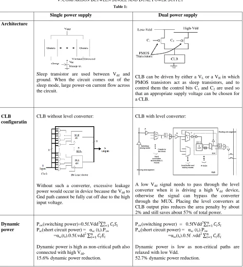
[image:4.612.59.558.142.690.2]V.COMPARISON BETWEEN SINGLE AND DUAL POWER SUPPLY Table 1:
Single power supply Dual power supply Architecture
Sleep transistor are used between Vdd and
ground. When the circuit comes out of the sleep mode, large power-on current flow across the circuit.
CLB can be driven by either a VL or a VH in which
PMOS transistors act as sleep transistors, and to control them the control bits C1 and C2 are used so
that an appropriate supply voltage can be chosen for a CLB.
CLB configuratin
CLB without level converter:
Without such a converter, excessive leakage power would occur in device because the Vdd to
Gnd path cannot be fully cut off due to the high input voltage.
CLB with level converter:
A low Vdd signal needs to pass through the level
converter when it is driving a high Vdd device,
otherwise the signal can bypass the converter through the MUX. Placing the level converters at CLB output pins reduces the area penalty by about 2% and still saves about 57% of total power.
Dynamic power
Psw(switching power)=0.5f.Vdd2∑ Psc(short circuit power) = αsc (tr).Psw
=αsc(tr).0.5f.vdd2 ∑
Dynamic power is high as non-critical path also connected with high Vdd.
15.6% dynamic power reduction.
Psw(switching power) = 0.5fVdd2∑ Psc(short circuit power) = αsc (tr).Psw
=αsc(tr).0.5f .vdd2 ∑
Dynamic power is low as non-critical paths are relaxed with low Vdd.
International Journal of Emerging Technology and Advanced Engineering
Website: www.ijetae.com (ISSN 2250-2459,ISO 9001:2008 Certified Journal, Volume 4, Issue 2, February 2014)
849
VI. CONCLUSION
We have presented LUT-based a single-Vdd as well as dual-Vdd FPGA architecture that optimize dynamic power, leakage power and interconnect power. Then, we have compared single-Vdd and dual-Vdd for different parameter such as power, area and delay. We also presented single-Vdd and dual-single-Vdd mapping algorithm to minimize the power and area. We shown that our dual-Vdd mapping algorithm can further improve total power compared to the early single-Vdd version and dual-Vdd is better for total power reduction of 12.8% over Single-Vdd mapping algorithm.
REFERENCES
[1] Deming Chen, Jason Cong, Chen Dong, Lei He, Fei Li and Chi-Chen Peng, “Technology Mapping and Clustering for FPGA Architectures with Dual Supply Voltages”, IEEE Trans.CAD, vol. 29, no. 11, Nov.2010.
[2] F. Li, Y. Lin, L. He, D. Chen, and J. Cong, “Power modeling and characteristics of field programmable gate arrays,” IEEE Trans. CAD, vol. 24, no. 11, Nov. 2005.
[3] F. Li, Y. Lin, and L. He, “Vdd programmability to reduce FPGA interconnect power,” in Proc. Int. Conf. Comput.-Aided Design, Nov. 2004.
[4] D. Chen and J. Cong, “DAOmap: A depth-optimal area optimization mapping algorithm for FPGA designs,” in Proc. Int. Conf. Comput.- Aided Design, Nov. 2004.
[5] D. Chen, J. Cong, F. Li, and L. He,“Low-power technology mapping for FPGA architectures with dual supply voltages,” in Proc. Int. Symp. FPGA, Feb. 2004.
[6] D. Chen and J. Cong, “Delay optimal low-power circuit clustering for FPGAs with dual supply voltages,” in Proc. Int. Symp. Low Power Electron. Design, 2004.
[7] F. Li, Y. Lin, and L. He, “FPGA power reduction using configurable dual-Vdd,” in Proc. Design Automat. Conf., Jun. 2004.
[8] K. K. W. Poon, A. Yan, and S. J. E. Wilton, “A flexible power model for FPGAs,” in Proc. Int. Conf. Field-Programm. Logic Applicat., Sep. 2002.
Leakage power
Pleakage(i) = Ileakage(Vdd).Vdd
Leakage power is dissipated in both the used and the unused part of the FPGA. Circuit blocks are always in active mode due to this leakage power is high.
Pleakage(i) = Ileakage(Vdd).Vdd
Leakage power is reduced because sleep transistors are ON when a circuit is active and are turned OFF when the circuit is in standby mode, effectively limiting the leakage current from supply to ground. In sleep mode, leakage of a circuit block reduces to 10% of high Vdd leakage.
FPGA area Efficiency
Level converter are not used in single-Vdd due
to this, Area of logic blocks in single-Vdd is less
than dual-Vdd .
Due to the area overhead of level converters and supply transistors, the dual-Vdd FPGA takes
approximately 21% more area than a single-Vdd.
Delay minimization
Delay is less as no level converter is used in single-Vdd.
The Level converter delay is almost 17% of the delay of an LUT when a VH of 1.1V and VL of 0.9V are
used so more is provided in Dual-Vdd.