International Journal of Emerging Technology and Advanced Engineering
Website: www.ijetae.com (ISSN 2250-2459,ISO 9001:2008 Certified Journal, Volume 3, Issue 12, December 2013)
205
An Approach for Realization of 2‘s Complement Adder
Subtractor Using DKG Reversible Gate
Shefali Mamataj
1, Biswajit Das
2, Anurima Rahaman
31
Assistant Professor, Department of ECE, Murshidabad College of Engineering &Technology
2Assistant Professor,Department of CSE , Murshidabad College of Engineering &Technology
3Student, Department of AEIE, Future Institute of Engineering and Management
Abstract— Reversible logic is one of the most important issue at present time and it has different areas for its application. The main purposes of designing reversible logic are to decrease quantum cost, depth of the circuits and the number of garbage outputs This paper represents an another approach to realize 4 bit 2’s complement adder subtractor by using reversible logic gates like Feynman Gate, DKG gate and one control line. A also a new reversible gate DKFG is proposed.
Keywords—Reversible logic, Basic Reversible Gates, 2’s Complement , Reversible full adder, Reversible full sub -tractor , Garbage ,Quantum cost.
I. INTRODUCTION
In electronics hardware designing energy dissipation is one of the most important aspects. The concept of reversibility in digital circuits is firstly related to energy by Landauer in 1961 who stated that there is small amount of heat dissipation the circuit due to loss of one bit of information and it would be equal to kTln2 where ‗k‘ is Boltzman constant and T is the temperature[1] . Also in 1973 it was proved by Bennett that the energy kTln2 would not be dissipate from the circuit if input can be extracted from output and it would be possible if and only if reversible gates are used[2]. According to Moore‘s law the numbers of transistors will double every 18 months. Thus energy conservative devices are the need of the day. The amount of energy dissipated in a system bears a direct relationship to the number of bits erased during computation. Reversible circuits are those circuits that do not lose information A circuit will be reversible if input vector can be specifically retrieved from output vectors and here is one to one correspondence between input and output [3]. A reversible logic circuit should have the following features [5]:
• Use minimum number of reversible gates. • Use minimum number of garbage outputs. • Use minimum constant inputs.
II. BASIC REVERSIBLE LOGIC GATES
A.
Reversible logic Function:
It is an n-input n-output logic function in which there is a one-to-one correspondence between the inputs and the outputs. Because of this bijective mapping the input vector can be uniquely determined from the output vector. This prevents the loss of information which is the root cause of power dissipation in irreversible logic circuits. The reversible logic circuits must be constructed under two main constraints. They are
Fan-out is not permitted.
Loops or feedbacks are not permitted
The quantum cost(QC) of any reversible gate(circuit) is the number of 1×1 or 2×2 reversible gates and quantum logic gates such as V, V+ (V is also named square root of
NOT gate NOT and V+ is hermitian of V). The V and V+
quantum gates have some properties that are shown in Equation (1) (Mohammadi et al., 2009).
V ×V = NOT
V ×V+= V+ × V= I Equation (1)
V+ ×V+ = NOT
Any reversible logic gate (circuit) is realized by using mentioned gates above, NOT and FG gates. The properties above show that when two V gates are in series they will behave as a NOT gate. Similarly, two V + gates in series also function as a NOT gate. A V gate in series with V + gate, and vice versa, is an identity.
B.
Basic Reversible logic GatesInternational Journal of Emerging Technology and Advanced Engineering
Website: www.ijetae.com (ISSN 2250-2459,ISO 9001:2008 Certified Journal, Volume 3, Issue 12, December 2013)
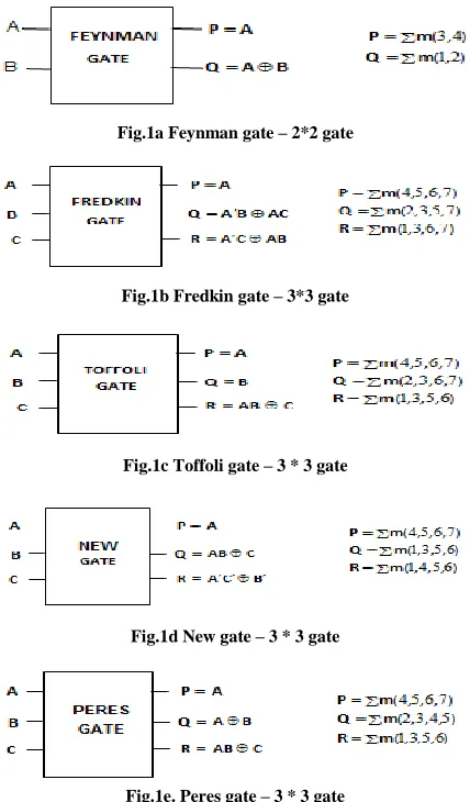
[image:2.612.348.544.126.335.2]206 There is also a double Feynman gate [7], Fredkin gate [8] and Toffoli gate [9], New Gate[10] , Peres gate[11] , all of which can be used to realize important combinational functions and all are 3*3 reversible gates and are as shown in the figure.1b to figure.1e .The figures also shows the switching functions for terminals.
Fig.1a Feynman gate – 2*2 gate
Fig.1b Fredkin gate – 3*3 gate
Fig.1c Toffoli gate – 3 * 3 gate
Fig.1d New gate – 3 * 3 gate
Fig.1e. Peres gate – 3 * 3 gate
There are other 4*4 gates some of which are specially designed for the realization of important combinational circuit functions in addition to some basic functions. Some of the important 4*4 gates are, TSG gate [13],MKG gate [12],HNG gate [14]etc, shown in figure(2a,2b,2c) all of which are very useful for the construction of important reversible adders.
Fig 2a: Block diagram of MKG Gate
Fig 2b: Block diagram of HNG Gate
Figure 2c: TSG Gate Block diagram
C.
Reversible logic DKG gate[image:2.612.61.275.209.574.2]
A 4* 4 reversible DKG gate [4] shown in Fig 3a. It can work singly as a reversible Full adder and a reversible Full subtractor is shown in Fig 3b and Fig 3c. It can be verified that input pattern corresponding to a particular output pattern can be uniquely determined. If input A=0, gate works as a reversible Full adder, and if input A=1, then it works as a reversible Full subtractor. It has been proved that a reversible full-adder circuit requires at least two garbage outputs to make the output combinations unique [15], [4].
Fig 3a: DKG reversible gate
[image:2.612.326.559.499.655.2]International Journal of Emerging Technology and Advanced Engineering
Website: www.ijetae.com (ISSN 2250-2459,ISO 9001:2008 Certified Journal, Volume 3, Issue 12, December 2013)
207
Fig 3c: DKG gate implemented as Full subtractor
C.
2’s Complement Adder Subtractor Circuit ArchitectureThe operations of addition and subtraction of signed/unsigned numbers can be performed using only the addition operations if 2‘s complement form is used to represent negative numbers. The 2‘s complement Adder Subtractor circuit is based on block diagram as shown in Fig. 4, which consists of XOR and full adder circuit (Mano and Ciletti, 2006). XOR is implemented as a complementary system with input M as a controller. M is connected to Cin to perform the 2‘s complement process. In
LOW state of M, XOR past the B-number to the full adder and the circuit performs addition of the A and B numbers. When the M level is HIGH, XOR invert the B-number and Cin = 1 will add with B’ to complete the 2‘s complement.
[image:3.612.328.561.252.570.2]Then, full adder circuit adds the 2‘s complement of B with the A-number. This operation shows that when M = 1, the circuit subtracts B-number from the A-number.
Fig 4 .2’s complement 4-bit parallel binary adder-subtractor
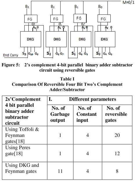
III. REALIZATION OF 2‘SCOMPLEMENT ADDER SUBTRACTOR CIRCUIT BY REVERSIBLE DKG AND
FEYNMAN GATE
We have realized 2‘s complement adder subtractor circuit by using FG and DKG reversible gates where a control line M is also used which is shown in Fig 5 .DKG reversible gate is used as a full adder[15] and FG reversible gate is used as XOR gate by setting one input M=0/1.When M=0 we get B0 =B000 and first DKG as a full adder adds A0,
B0 and 0.
And we get the sum S0 as a addition result and the
generated carry is forwarded to the next DKG and so on. In this way the circuit performs as a parallel adder. But when M=1 we get the output of first FG is B‘0 and 1.So the
first DKG adds A0,B‘o and 1.So it performs A0+
(B‘0+1)=A0+(2‘s complement of B)=A0-B0.And the borrow
generated is forwarded to the next DKG and so on. So finally we can see that DKG performs subtraction by 2‘s complement method.
Figure 5: 2’s complement 4-bit parallel binary adder subtractor circuit using reversible gates
Table I
Comparison Of Reversible Four Bit Two’s Complement Adder/Subtractor
2s’Complement 4 bit parallel binary adder subtractor circuit
I. Different parameters
No. of Garbage output
No. of Constant input
No. of reversible gates
Using Toffoli & Feynman gates[18]
1 4 20
Using Peres
gate[18] 1 4 12
Using DKG and
Feynman gates 11 4 8
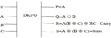
IV. PROPOSED 4*4REVERSIBLE GATE
[image:3.612.53.284.424.554.2]International Journal of Emerging Technology and Advanced Engineering
Website: www.ijetae.com (ISSN 2250-2459,ISO 9001:2008 Certified Journal, Volume 3, Issue 12, December 2013)
[image:4.612.355.538.144.224.2]208
Figure 6 : DKFG Gate
[image:4.612.54.279.149.344.2]We can use DKFG gate as a full-adder as shown in figure 7a.
Fig 7a.Implementation of DKFG gate as a full-adder
[image:4.612.345.559.278.355.2]The proposed DKFG gate can implement the conventional Boolean functions. Realization of AND operation, XOR operation, NOT operation and XNOR operation and also COPY operation shown in figure 8b and 8c
Fig 7b.Implementation of DKFG gate as AND, XOR, COPY operations
Fig 7c.Implementation of DKFG gate as NOT, XOR, XNOR operations
We can implement half-adder by using DKFG gate as shown in figure 7d.
Fig 7d.Implementation of DKFG gate as a full-adder
V. CONCLUSION
We have realized 2‘s complement adder-subtractor circuit by using FG and DKG reversible gates and made a comparisons in TABLE1.Also the proposed reversible DKFG gate has been used to implement different types of logical operations including combinational circuits – Full Adder, Half Adder using a single gate. Also it can be further used to implement reversible Ripple Carry Adder and many other computational circuits.
REFERENCES
[1 ] R. Landauer, ―Irreversibility and Heat Generation in the computational Process, IBM Journal of Research and Development, 5, pp. 183-191, 1961.
[2 ] C.H. Bennett, Logical Reversibility of Computation‖, IBM J.Research and Development, pp. 525-532, November 1973. [3 ] Pradeep singla and Naveen kr. Malik ― A Cost - Effective Design of
Reversible programmable logic array‖ International Journal Of Computer Application , volume 41 – no. 15, march- 2012. [4 ] ‖A novel design of reversible serial and parallel adder/subtractor‖ in
International journal of engineering science and technology by Krishnaveni.D and Geetha priya.M.
[5 ] Perkowski, M. and P. Kerntopf, ―Reversible Logic. Invited tutorial‖, Proc. EURO-MICRO, Sept 2001, Warsaw, Poland.
[image:4.612.70.263.396.463.2] [image:4.612.76.266.555.626.2]International Journal of Emerging Technology and Advanced Engineering
Website: www.ijetae.com (ISSN 2250-2459,ISO 9001:2008 Certified Journal, Volume 3, Issue 12, December 2013)
209 [7 ] B. Parhami; ―Fault Tolerant Reversible Circuits‖ Proc. 40th
Asilomar Conf. Signals, Systems, and Computers, Pacific Grove,CA, Oct.2006.
[8 ] E. Fredkin, T. Toffoli, ―Conservative Logic‖,International Journal of Theor. Physics, 21, 1982, pp.219-253.
[9 ] T. Toffoli., ―Reversible Computing‖, Tech memo MIT/LCS/TM‐151, MIT Lab for Computer Science (1980). [10 ]Md. M. H Azad Khan, ―Design of Full-adder With Reversible
Gates‖, International Conference on Computerand Information Technology,Dhaka, Bangladesh, 2002,pp.515-519.
[11 ]Peres, A., 1985. Reversible logic and quantum computers, Physical Review: A, 32 (6): 3266-3276.
[12 ]Haghparast, M. and K. Navi, 2007. A Novel Reversible Full Adder Circuit for Nanotechnology Based Systems. J. Applied Sci., 7 (24): 3995-4000.
[13 ]Thapliyal H., S. Kotiyal, M. B. Srinivas, 2006.Novel BCD adders and their reversible logic implementation for IEEE 754r format. Proceedings of the 19th International Conference on VLSI Design, 3-7 Jan 2006.
[14 ]Haghparast M. and K. Navi, 2008. A Novel reversible BCD adder for nanotechnology based systems. Am. J. Applied Sci., 5(3): 282-288.
[15 ]‖Optimal design of a reversible full adder‖ in International Journal of unconventional computing by Yvan Van Rentergen and Alexis De Vos
[16 ]‖A novel design of reversible serial and parallel adder/subtractor‖ in International journal of engineering science and technology By Krishnaveni.D and Geetha priya.M.
[17 ]Parallel adders from Google website.