Article
Continuous-Input Continuous-Output Current
Buck-Boost DC
/
DC Converters for Renewable
Energy Applications: Modelling and
Performance Assessment
Nahla E. Zakzouk1, Ahmed K. Khamis1, Ahmed K. Abdelsalam1,* and Barry W. Williams2
1 Electrical and Control Engineering Department, Arab Academy for Science,
Technology and Maritime Transport, Alexandria 1029, Egypt; [email protected] (N.E.Z.); [email protected] (A.K.K.)
2 Electronics and Electrical Engineering Department, Strathclyde University, Glasgow G11XW, UK;
* Correspondence: [email protected]
Received: 21 April 2019; Accepted: 27 May 2019; Published: 10 June 2019
Abstract: Stand-alone/grid connected renewable energy systems (RESs) require direct current (DC)/DC converters with continuous-input continuous-output current capabilities as maximum power point tracking (MPPT) converters. The continuous-input current feature minimizes the extracted power ripples while the continuous-output current offers non-pulsating power to the storage batteries/DC-link. CUK, D1 and D2 DC/DC converters are highly competitive candidates for this task especially because they share similar low-component count and functionality. Although these converters are of high resemblance, their performance assessment has not been previously compared. In this paper, a detailed comparison between the previously mentioned converters is carried out as several aspects should be addressed, mainly the converter tracking efficiency, conversion efficiency, inductor loss, system modelling, transient and steady-state performance. First, average model and dynamic analysis of the three converters are derived. Then, D1 and D2 small signal analysis in voltage-fed-mode is originated and compared to that of CUK in order to address the nature of converters’ response to small system changes. Finally, the effect of converters’ inductance variation on their performance is studied using rigorous simulation and experimental implementation under varying operating conditions. The assessment finally revels that D1 converter achieves the best overall efficiency with minimal inductor value.
Keywords: continuous-input current; continuous-output current; buck-boost; DC/DC converters; renewable energy system; photovoltaic; MPPT; dynamic modelling; and small-signal analysis
1. Introduction
The world’s increasing energy consumption, depleting fossil fuels, global warming concerns and environmental problems have greatly increased the interest in clean renewable energy sources recently [1]. Wind energy forms one of the best candidates due to its high power penetration capabilities [2]. Photovoltaic (PV) solar energy has become a promising renewable/alternate energy source due to several advantages such as absence of noise or mechanical moving parts, low operation cost, no emission of CO2or other harmful gases, flexibility in size, and its convenience in arid areas [1–3].
The non-linear behavior and dependency of almost all renewable energy sources on the atmospheric conditions create one of the main challenges facing the renewable energy sector’s penetration of the energy market [4,5]. To minimize these drawbacks, renewable energy systems (RESs) operation at
the maximum power point is a necessity. Consequently, a switched-mode power electronic converter, called a “maximum power point tracker”, must be placed between the RES terminals and the load [6]. Various maximum power point tracking (MPPT) techniques have been developed to maximize the RES extracted power efficiently [7–9]. These converters can be placed in standalone or two-stage grid tied configurations [8–11].
Buck-boost direct current (DC)/DC converters are commonly applied as RES MPPT converters. However, the basic buck-boost converters suffer from discontinuous input current [12,13] resulting in discontinuous RES current, thus deteriorating the MPPT process. To overcome the latter, a large electrolytic capacitor filter buffer is applied at the converter input yet at the penalty of added extra cost, weight, electrical resonance issues and less system reliability [14]. Fortunately, these shortcomings can be eliminated if the conversion input stage draws continuous and controllable input current that allows the RES’s maximum power point to be closely tracked, with minimal current/voltage ripple (i.e., power ripple) [15].
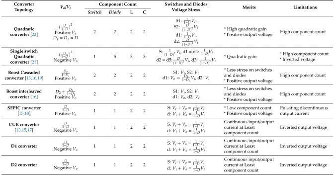
A number of continuous-input-current buck-boost DC-DC converters have been developed [15–22] as shown in Table1, see AppendixAfor converters’ realization. These converters can be extensively used for maximum utilization of RES as wind and PV systems. Quadratic buck-boost converters have the merit of high quadratic gain expanding system voltage levels; however, at the cost of high component count [21,22]. Boost-cascaded and Boost-interleaved buck-boost converters show low switch and diode stress but again at the cost of high component count increasing switching losses and converter cost [15,16,19]. CUK and SEPIC serve as promising buck-boost converters with the merits of continuous-input-current at the least component count [13,15,17,18]. However, SEPIC shows pulsating output current that can be smoothed out using additional output filter which increases system size and losses [20]. Hence, from the non-pulsating input and output current with the least component count perspective, CUK is a good candidate for versatile standalone/grid integrated RES applications with different voltage levels and various loads nature. With similar merits as CUK including component count, D1 and D2 buck-boost converters are introduced in [23], and tested with fixed input DC sources. These DC/DC converters behave as current-sourced converters, which are topological duals of the buck-boost voltage-sourced converters [24].
Although the three converters (CUK, D1 and D2) resemble each other in many aspects (defined in Table1), they can show differences especially when being applied with RES as maximum power point trackers (MPPTs). Besides experiencing different power conversion efficiencies, they also differ in tracking efficiency. Hereby, not only the converter losses affect the converter overall efficiency but the input current ripples play an important role [25]. The latter affects the tracked RES power ripples, which impact the converter power tracking efficiency. Moreover, system small changes and ripples can affect converters’ output voltage; hence it is a point that should be addressed. Finally, the converters’ tolerance to inductances variation has significant impact on their performance and should be taken into account. Increasing converter inductances minimizes converter input-current-ripples, thus improving its tracking efficiency, but meanwhile increases converter inductor losses, which downgrades its conversion efficiency.
Table 1.Comparison between most recent continuous-input-current buck-boost direct current (DC)/DC converters.
Converter
Topology Vo/Vi
Component Count Switches and Diodes
Voltage Stress Merits Limitations
Switch Diode L C
Quadratic converter[22]
(1−DD)2 PositiveVo
D1=D2=D
2 2 2 2
S1: 1−1DVi, S2: D
(1−D)2Vi
d1: 1−1DVi, d2: D
(1−D)2Vi
* High quadratic gain
* Positive output voltage High component count
Single switch Quadratic converter[21]
(1−DD)2 NegativeVo
1 5 3 3
S: 1
(1−D)2Vi, d1=d4: 1 1−DVi
d2=d5: D
(1−D)2Vi, d3: 1 (1−D)2Vi
* Quadratic gain * High component count * Inverted voltage
Boost Cascaded converter[15,16,19]
D2
1−D1
PositiveVo 2 2 2 2
S1:Vi, S2:Vi d1:Vo= 1−D2D1Vi, d2:Vi
* Less stress on switches and diodes
* Positive output voltage
High component count
Boost interleaved converter[16]
D2+1−D1D1
PositiveVo 2 2 2 2
S1:Vi, S2:Vi d1:Vo, d2:Vi
* Less stress on switches and diodes
* Positive output voltage
High component count
SEPIC converter [15,18]
D
1−D
PositiveVo 1 1 2 2
S:Vi+Vo= 1−1DVi d:Vi+Vo=1−1DVi
* Low component count * Positive output voltage
Pulsating discontinuous output current
CUK converter [13,15,17]
D
1−D
NegativeVo 1 1 2 2
S:Vi+Vo= 1−1DVi d:Vi+Vo=1−1DVi
Continuous input/output current at Least
component count
Inverted output voltage
D1 converter
D
1−D
NegativeVo 1 1 2 2
S:Vi+Vo= 1−1DVi d:Vi+Vo=1−1DVi
Continuous input/output current at Least
component count
Inverted output voltage
D2 converter
D
1−D
NegativeVo 1 1 2 2
S:Vi+Vo= 1−1DVi d:Vi+Vo=1−1DVi
Continuous input/output current at Least
component count
2. Average Circuit Modelling for the Considered Buck-Boost Converters
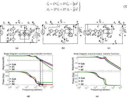
Modelling of the three considered buck-boost choppers in the inductor continuous current mode (CCM) is presented using the average model as shown in Figure1. Voltage and current gains are derived for each converter along with dynamic analysis of each converter as follows:Energies 2019, 12, x FOR PEER REVIEW 4 of 28
Figure 1. Circuit topology for: (a) CUK; (b) D1; (c) D2 converters.
2.1. CUK Converter
For the CUK converter shown in Figure 1a, the following analysis is carried out; The average capacitor current Ic = 0,
∴ −𝑰𝑳𝒐(𝐷𝑇) + 𝑰𝑳𝒊(1 − 𝐷)𝑇 = 0 ∴ 𝑰𝑰𝑳𝒊
𝑳𝒐= 𝐷 (1 − 𝐷)
(1)
2.1.1. Voltage Transfer Function Calculation
The average input current Ii = ILi, while the average output current Io= ILo, hence; 𝑰
𝑰 =
𝐷
[image:4.595.92.510.165.638.2](1 − 𝐷) (2)
Figure 1.Circuit topology for: (a) CUK; (b) D1; (c) D2 converters.
2.1. CUK Converter
For the CUK converter shown in Figure1a, the following analysis is carried out; The average capacitor currentIc=0,
∴ −ILo(DT) +ILi(1−D)T=0
∴ ILi ILo =
D
(1−D)
2.1.1. Voltage Transfer Function Calculation
The average input currentIi=ILi, while the average output currentIo=ILo, hence;
Ii
Io
= D
(1−D) (2)
Note that Iohas an opposite direction.
Average input powerPi=Average output powerPo,
∴ViIi=VoIo
∴ Vo Vi =
Ii Io =
D
(1−D)
(3)
Note that Vohas an opposite polarity.
2.1.2. Inductors’ Ripple Currents Calculation
When the switchSis closed;
vLi =Li∆∆itLi =Li∆DTiLi =Vi
∴∆iLi= ViLDTi = ViD fswLi
(4)
vLo =vC−Vo=VC±∆vC−Vo (5)
Since, average of inductor voltages=0
∴ VC−Vo=Vi (6)
Substitute (6) in (5)
∴vLo =Vi±∆vc, ∆vCVi
∴vLo=Lo∆∆iLot =Lo∆DTiLo ≈Vi
∴∆iLo= ViLDTo = ViD fswLo
(7)
2.1.3. Input/Output Ripple Currents Calculation
∆ii=∆iLi = ViLDTi ∆io=∆iLo= ViLoDT
(8)
2.2. D1 Converter
For D1 converter shown in Figure1b, the following analysis is carried out; The average capacitor currentIc=0,
∴ (ILi−ILo)(DT) +ILi(1−D)T=0 ∴ ILi
(ILo−ILi) = D
(1−D)
(9)
2.2.1. Voltage Transfer Function Calculation
The average input currentIi=ILiwhile the average output currentIo=ILo−ILi, hence
Ii
Io
= D
Note thatIohas an opposite direction.
Average input powerPi=Average output powerPo, hence
∴ViIi=VoIo
∴ Vo Vi =
Ii Io =
D
(1−D)
(11)
Note thatVohas an opposite polarity.
2.2.2. Inductors’ Ripple Currents Calculation
When the switch S is closed;
vLi=Vi+Vo−vc=Vi+Vo−(VC±∆vC) (12)
Since average of inductor voltages=0
∴Vi+ Vo−VC=0 (13)
Substitute (13) in (12)
∴vLi =∓∆vc
∴vLi =Li∆∆iLit =Li∆DTiLi =∓∆vc
∴∆iLi =
∓∆vcDT
Li =
∓∆vcD
fswLi
(14)
Regarding voltage ripples of the output inductor
vLo=Vi−vLi (15)
From (14);
vLo =Vi±∆vc, ∆vC Vi ∴vLo=Lo∆∆iLot =Lo∆DTiLo ≈Vi
∴∆iLo= ViLoDT = fVswiDLo
(16)
2.2.3. Input/Output Ripple Currents Calculation
∆ii=∆iLi =
∓∆vcDT
Li ∆io=∆iLo−∆iLi = ViLDTo −(∓
∆vcDT Li )
(17)
2.3. D2 Converter
For the D2 converter shown in Figure1c, the following analysis is carried out; The average capacitor currentIc=0,
∴ −ILo(DT) + (ILI−ILo)(1−D)T=0
∴ ILi−ILo
ILo = (1−DD)
(18)
2.3.1. Voltage Transfer Function Calculation
The average input currentIi=ILi−ILowhile the average output currentIo=ILo, hence
Ii
Io
= D
Note that Iohas an opposite direction.
Average input powerPi=Average output powerPo, hence
∴ViIi=VoIo
∴ Vo Vi =
Ii Io =
D
(1−D)
(20)
Note that Vohas an opposite direction.
2.3.2. Inductors’ Ripple Currents Calculation
When the switch S is closed;
vLi =Li∆∆iLit =Li∆DTiLi =Vi
∴∆iLi= ViLDTi = fswLViDi
(21)
vLo =vC−Vo−Vi=VC±∆vC−Vo− Vi (22)
Since average of inductor voltages=0
∴ VC−Vo−Vi =0 (23)
Substitute (23) in (22)
∴vLo=±∆vC
∴vLo =Lo∆∆iLot =Lo∆DTiLo =±∆vC
∴∆iLo=
±∆vCDT
Lo =
±∆vCDT
fswLo
(24)
2.3.3. Input/output Ripple Currents Calculation
∆ii=∆iLi−∆iLo= ViLDTi −(±∆vLoCDT) ∆io =∆iLo=
±∆vCDT
Lo
(25)
In all cases, when S is closed;ic=−io
∴∆vC= 1 C
Z DT
0
−iodt≈ −IoDT
C (26)
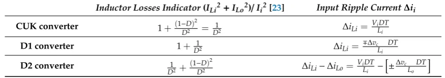
D1, D2 and CUK are common in many aspects, as shown in Table1, however they differ in efficiency. DC/DC power converter conversion efficiency (ζconv.= Output power to loadInput DC power )is a dominant aspect to evaluate converter performance. However, for the converters under consideration, the input is commonly a RES in which the converter input voltage and current are controlled to track the maximum power. This results in RES current and voltage ripples and, in turn, extracted power oscillations which affect the converter MPPT performance. Hence, another efficiency aspect rises which can even show more importance than the converter power conversion efficiency. This is the converter tracking efficiency.
Table2summarizes the considered converters’ performances, derived in this section, regarding efficiency. The input current ripples affect the extracted RES power value which reflects directly in the converter tracking efficiency. While inductor copper losses affect converters’ losses which mirror converter power conversion efficiency. Referring to Table2, CUK shows highest conversion efficiency since it experiences the least inductors’ copper losses while D1 shows highest tracking efficiency since it has the least input current ripple. D2 shows better tracking efficiency than CUK but poorer tracking efficiency than D1. To find out the optimal converter to use, converters’ performances will be compared, in simulation and practically, regarding their overall efficiencies;
ζtotal= Output power to load
[image:8.595.79.515.276.353.2]Available maximum RES power at same conditions =ζMPPT.ζconv (27)
Table 2.Aspects considered for converter efficiency assessment.
Inductor Losses Indicator(ILi2+ILo2)/Ii2[23] Input Ripple Current∆ii CUK converter 1+(1−D)
2
D2 =D12 ∆iLi=
ViDT
Li
D1 converter 1+ 1
D2 ∆iLi=
∓∆vc DT
Li
D2 converter 1
D2+ (1−D)2
D2 ∆iLi−∆iLo=
ViDT
Li
−h±∆vc DT
Lo
i
3. Small Signal Model for the Considered Buck-Boost Converters in Continuous Current Mode (CCM)
The small signal model of CUK in inductor CCM is derived in using the circuit averaging technique [26,27]. Accordingly, small signal models for D1 and D2 in CCM are originally derived in this paper and their relative control-to-output voltage and input-to-output voltage transfer functions are then computed and compared in voltage-fed-mode as follows.
In order to obtain converters’ small signal model, small signal ac terms should be included as follows;
Dtot=D+Dˆ, vi=Vi+vˆi, vo=Vo+vˆo, iLi=ILi+iLiˆ, iLo=ILo+iLoˆ
(28)
3.1. CUK Converter
The average diode current (Id) and the average MOSFET voltage (VS) are given by:
Id= T1 T R
DT
(ILi+ILo)dt= (ILi+ILo)(1−D)
VS= 1T T R
DT
VCdt= 1T T R
DT
(Vi+Vo)dt= (Vi+Vo)(1−D)
(29)
To obtain CUK converter small signal model, substitute (28) in (29) and lettingD’=1 –D;
Id+iˆd= (1−Dtot)(iLi+iLo) = (D0−dˆ)(ILi+iˆLi+ILo+ iLoˆ )
VS+vˆS = (1−Dtot)(vi+vo) = (D0−dˆ)(Vi+vˆi+Vo+ vˆo)
Using the facts thatVoVi = Ii Io =
D
D0 and that in CUKILi=IiandILo =Io, then after manipulations,
(31) results;
Id+iˆd=ILo−IDLo0dˆ+D 0 ˆ
iLi+D0iLoˆ −dˆiLiˆ −dˆiLoˆ
VS+vˆS=Vi−DVi0dˆ+D 0
ˆ
vi+D0vˆo−dˆvˆi−dˆvˆo
(31)
Considering small signal model, only small signal ac components are extracted (average quantities are excluded). Furthermore, high order non-linear ac terms are neglected since ˆdD, ˆviVi, ˆiLi ILi, ˆiLo ILo. Hence, (32) can be obtained and CUK small signal model in CCM is demonstrated in Figure2a, whereZLi=RLi+sLi, ZLo=RLo+sLo, ZC= sC1, Zo=Rok sCo1
ˆ
id=D0iLiˆ +D0iLoˆ −IDLo0dˆ
ˆ
vS =D0vˆi+D0vˆo−DVi0dˆ
(32)
Energies 2019, 12, x FOR PEER REVIEW 9 of 28
𝐷, 𝑣 ≪ 𝑉 , 𝚤 ≪ 𝐼 , 𝚤 ≪ 𝐼 . Hence, (32) can be obtained and CUK small signal model in CCM is
demonstrated in Figure 2a, where 𝑍 = 𝑅 + 𝑠𝐿 , 𝑍 = 𝑅 + 𝑠𝐿 , 𝑍 = , 𝑍 = 𝑅 ‖
Figure 2. Converters’ small signal models in continuous current mode (CCM): (a) CUK model; (b) D1 model; (c) D2 model; (d) Bode plot of control-to-output and (d) input-to-output transfer functions for the three investigated converters.
𝚤 = 𝐷 𝚤 + 𝐷 𝚤 −𝐼
𝐷 𝑑
𝑣 = 𝐷 𝑣 + 𝐷 𝑣 −𝑉
𝐷 𝑑
(32)
3.1.1. To Get Control-to-Output Transfer Function
Set 𝑣 = 0, small signal voltage and current of 𝑍 are given by:
𝑣 =𝑉
𝐷 𝑑 − 𝐷 𝑣 𝚤 =𝑣𝑍 =𝑍 𝐷𝑉 𝑑 −𝑍𝐷 𝑣 ⎭⎬
⎫
(33)
Small signal voltage and current of 𝑍 are given by:
𝚤 = 𝚤 =𝑣
𝑍
𝑣 = 𝑍 𝚤 =𝑍
𝑍 𝑣 ⎭⎬ ⎫
(34)
Small signal voltage and current of 𝑍 are given by:
𝚤 = 𝚤 − 𝚤 = 𝐷 𝚤 + 𝐷 𝚤 −𝐼𝐷 𝑑 − 𝚤
= 𝐷 𝚤 − 𝐷𝚤 −𝐼
𝐷 𝑑
𝑣 = 𝑍 𝚤 = 𝑍 𝐷 𝚤 − 𝑍 𝐷𝚤 −𝑍 𝐼𝐷 𝑑 ⎭⎪ ⎬ ⎪ ⎫
[image:9.595.86.514.214.547.2](35)
Figure 2.Converters’ small signal models in continuous current mode (CCM): (a) CUK model; (b) D1 model; (c) D2 model; (d) Bode plot of control-to-output and (d) input-to-output transfer functions for the three investigated converters.
3.1.1. To Get Control-to-Output Transfer Function
Set ˆvi=0, small signal voltage and current ofZLiare given by:
ˆ
vLi = DVi0dˆ−D 0
ˆ vo ˆ
iLi = ZvˆLiLi = Vi ZLiD0dˆ
− D0 ZLivˆo
(33)
Small signal voltage and current ofZLoare given by:
ˆ
iLo =iˆo = Zvoˆo
ˆ
vLo=ZLoiLoˆ = ZZLoovˆo
Small signal voltage and current ofZCare given by:
ˆ
iC=iˆd−iLoˆ =D0iˆLi+D0iLoˆ −IDLo0dˆ−iLoˆ
= D0iˆLi−DiLoˆ −DIo0dˆ
ˆ
vC=ZCiˆC=ZCD0iˆLi−ZCDiLoˆ −ZDC0Iodˆ
(35) Applying K.V.L; ˆ vC+ Vi
D0dˆ− vˆo−D 0
ˆ
vo− vˆLo=0 (36)
Substituting (33–35) in (36) and using the facts that VoVi = Ii Io =
D
D0 and Io = VoR
o =
DVi D0R
o, control-to-output transfer function results after some manipulations as shown in (37),
ˆ vo(s)
ˆ d(s) =
ZLiZoVi(1+D
0
ZC ZLi −
DZC D0R
o) D0
(D0
ZLiZo+ZLiZo+ZLiZLo+D02ZCZo+DZLiZC)
(37)
3.1.2. To Get Input-to-Output Transfer Function
Set ˆd=0, small signal voltage and current ofZLiare given by:
ˆ
vLi=vˆi−D0vˆi−D0vˆo =Dvˆi−D0vˆo ˆ
iLi= ZvˆLiLi = D ZLivˆi
− D0 ZLivˆo
(38)
Small signal voltage and current ofZLoare given by:
ˆ
iLo =iˆo = Zvoˆo
ˆ
vLo=ZLoiLoˆ = ZZLoovˆo (39)
Small signal voltage and current ofZCare given by:
ˆ
iC=iˆd−iLoˆ =D0iLiˆ +D0iLoˆ −iLoˆ = D0iˆLi−DiLoˆ
ˆ
vC=ZCiˆC=ZCD0iLiˆ −ZCDiLoˆ (40) Applying K.V.L; ˆ vC−D
0
ˆ vi−D
0
ˆ
vo− vˆo− vˆLo =0 (41)
Substituting (38–40) in (41) and after some manipulations, input-to-output transfer function results as shown in (42);
ˆ vo(s)
ˆ vi(s)
= DD
0
ZCZo− D0ZLiZo D0
ZLiZo+ZLiZo+ZLiZLo+D02ZCZo+DZLiZC
(42)
3.2. D1 Converter
The average diode current (Id) and the average MOSFET voltage (VS) are given by:
Id= T1 T R
DT
ILodt=ILo(1−D)
VS= 1T T R
DT
VCdt= 1T T R
DT
To obtain D1 converter small signal model, substitute (28) in (43) and lettingD’=1 –D;
Id+iˆd= (D
0− ˆ
d)(ILo+ iLoˆ ) VS+vˆS= (D
0− ˆ
d)(Vi+vˆi+Vo+ vˆo) (44)
Using the facts that VoV i =
Ii Io =
D
D0 and after some manipulations, (45) results;
Id+iˆd=D0ILo+D0iLoˆ −ILodˆ−dˆiLoˆ
VS+vˆS=Vi−DVi0dˆ+D 0
ˆ
vi+D0vˆo−dˆvˆi−dˆvˆo (45)
Considering small signal model, only small signal ac components are extracted (average quantities are excluded). Furthermore, high order nonlinear ac terms are neglected. Hence, (46) can be obtained and D1 small signal model in CCM is demonstrated in Figure2b:
ˆ
id=D0iLoˆ −ILodˆ
ˆ
vS =D0vˆi+D0vˆo−DVi0dˆ
(46)
3.2.1. To Get Control-to-Output Transfer Function
Set ˆvi=0, small signal voltage and current ofZLoare given by:
ˆ
iLo=iˆLi+iˆo =iLiˆ +Zovoˆ
ˆ
vLo =ZLoiLoˆ =ZLoiˆLi+ZZLoovˆo (47)
Small signal voltage and current ofZLiare given by:
ˆ
vLi= VD0idˆ−D 0
ˆ vo−vˆLo ˆ
iLi= ZvˆLiLi = Vi ZLiD0
ˆ d− D0
ZLivˆo −ZLo
ZLiiˆLi − ZLo
ZLiZovˆo
∴ iˆLi= D0 Vi (ZLi+ZLo)
ˆ d− (D
0
Zo+ZLo) Zo(ZLi+ZLo)vˆo
(48)
Small signal voltage and current ofZCare given by:
ˆ
iC=iˆd−iˆo=D0iLoˆ −iLodˆ−iˆo =D0(iˆLi+iˆo)−(Ii+Io)dˆ−iˆo
=D0iLiˆ −Diˆo−DIo0dˆ
ˆ
vC=ZCiˆC=ZCD0iLiˆ −ZCDiˆo−ZDC0Iodˆ
(49) Applying K.V.L; ˆ vC+ Vi
D0dˆ− vˆo−D 0
ˆ
vo− vˆLo=0 (50)
Substituting (47–49) in (50) and using the facts that VoVi = Ii Io =
D
D0 and Io = VoR
o =
DVi D0R
o, control-to-output transfer function results after some manipulations as shown in (51),
ˆ vo(s)
ˆ d(s) =
ViZo(D0ZC−ZLo)−DViZCZoD0(RZLi+ZLo)
o +ViZo(ZLi+ZLo) D0Z
3.2.2. To Get Input-to-Output Transfer Function
Set ˆd=0, small signal voltage and current ofZLoare given by:
ˆ
iLo=iˆLi+iˆo =iLiˆ +Zvˆoo
ˆ
vLo =ZLoiLoˆ =ZLoiˆLi+ZZoLovˆo (52)
Small signal voltage and current ofZLiare given by
ˆ
vLi =vˆi−D0vˆi−D0vˆo−vˆLo =Dvˆi−D0vˆo−vˆLo ˆ
iLi = ZvˆLiLi = D ZLivˆi−
D0
ZLivˆo− ZLo ZLiiLiˆ −
ZLo ZLiZovˆo
∴ iˆLi=
Dvˆi−D0voˆ−ZLoZovoˆ
(ZLi+ZLo)
(53)
Small signal voltage and current ofZCare given by:
ˆ
iC=iˆd−iˆo=D0iLoˆ −iˆo = D0 ˆ
iLi+D0iˆo−iˆo =D0iˆLi−Diˆo ˆ
vC=ZCiˆC=ZCD0iˆLi−ZCDiˆo (54) Applying K.V.L; ˆ vC−D
0
ˆ vi−D
0
ˆ
vo− vˆo− vˆLo =0 (55)
Substituting (52–54) in (55) and after some manipulations, input-to-output transfer function results as shown in (56);
ˆ vo(s)
ˆ vi(s)
= DZo(D
0
ZC−ZLo)− D0Zo(ZLi+ZLo)
Zo(1+D0)(ZLi+ZLo) + (DZC+ZLo)(ZLi+ZLo) + (D0ZC−ZLo)(D0Zo+ZLo)
(56)
3.3. D2 Converter
The average diode current (Id) and the average MOSFET voltage (VS) are given by:
Id= T1 T R
DT
ILidt=ILi(1−D)
VS= 1T T R
DT
VCdt= 1T T R
DT
(Vi+Vo)dt= (Vi+Vo)(1−D) (57)
To obtain D2 converter small signal model, substitute (28) in (57) and lettingD’=1−D;
Id+iˆd= (D0−dˆ)(ILi+iˆLi) VS+vˆS= (D0−dˆ)(Vi+vˆi+Vo+ vˆo)
(58)
Using the facts that VoV i =
Ii
Io = DD0 and after some manipulations, (59) results;
Id+iˆd=D0ILi+D0iˆLi−dIˆLi−dˆiˆLi
VS+vˆS=Vi−DVi0dˆ+D 0
ˆ
Considering small signal model, only small signal ac components are extracted (average quantities are excluded). Furthermore, high order nonlinear ac terms are neglected. Hence, (60) results and D2 small signal model in CCM is demonstrated in Figure2c:
ˆ id=D
0ˆ
iLi−ILidˆ
ˆ
vS =D0vˆi+D0vˆo−DVi0dˆ
(60)
3.3.1. To Get Control-to-output Transfer Function
Set ˆvi=0, small signal voltage and current ofZLiare given by:
ˆ
vLi = DVi0dˆ−D 0
ˆ vo ˆ
iLi = ZvˆLiLi = Vi ZLiD0
ˆ d− D0
ZLivˆo (61)
Small signal voltage and current ofZLoare given by:
ˆ
iLo =iˆo = Zvoˆo
ˆ
vLo=ZLoiLoˆ = ZZLoovˆo (62)
Small signal voltage and current ofZCare given by:
ˆ
iC=iˆd−iLoˆ =D0iLiˆ −ILidˆ−iLoˆ =D0iLiˆ −(Ii+Io)dˆ−iLoˆ
= D0iˆLi−iLoˆ −DIo0dˆ
ˆ
vC=ZCiˆC=ZCD0iLiˆ −ZCiLoˆ −ZDC0Iodˆ
(63) Applying K.V.L; ˆ
vC−vˆo− vˆLo =0 (64)
Substituting (61–63) in (64) and using the facts that VoV i =
Ii
Io = DD0 and Io = Vo
Ro = DVi D0
Ro, control-to-output transfer function results after some manipulations as shown in (65);
ˆ vo(s)
ˆ d(s) =
ViZCZo(1−DDZ02RoLi )
ZLi(ZC+ZLo+Zo) +D02ZCZo
(65)
3.3.2. To Get Input-to-Output Transfer Function
Set ˆd=0, small signal voltage and current ofZLiare given by:
ˆ
vLi=vˆi−D0vˆi−D0vˆo =Dvˆi−D0vˆo ˆ
iLi= ZvˆLiLi = D ZLivˆi
− D0 ZLivˆo
(66)
Small signal voltage and current ofZLoare given by:
ˆ
iLo =iˆo = Zovoˆ
ˆ
Small signal voltage and current ofZCare given by:
ˆ
iC=iˆd−iLoˆ =D0iˆLi−iLoˆ ˆ
vC=ZCiˆC=ZCD
0 ˆ
iLi−ZCiLoˆ
(68)
Applying K.V.L;
ˆ
vC− vˆi− vˆo− vˆLo=0 (69)
Substituting (66–68) in (69) and after some manipulations, input-to-output transfer function results as shown in (70)
ˆ vo(s)
ˆ vi(s)
= DD
0
ZCZo− ZLiZo ZLi(ZC+ZLo+Zo) +D02ZCZo
(70)
For voltage-fed-mode, Bode plots of converters’vˆo(s) ˆ d(s) and
ˆ vo(s)
ˆ
vi(s) are shown in Figure2d.
Regarding thevoˆdˆ((ss))Bode plot, high identical DC gain (50 dB) is achieved for the three converters which proves the capability of all converters to minimize the steady-state error during open-loop operation. Almost identical crossover frequency (frequency at 0 db gain) in both D1 and D2 converters atωc1, while CUK converter showed slightly higher frequency atωc2.This indicates the CUK converter’s capability of using a controller with higher bandwidth but meanwhile D1 and D2 converters show higher rejection capability to high frequency disturbances. Moreover, the latter showed that the CUK converter has to be operated at switching frequency higher than that of D1 and D2 converters since the converter switching frequency should be at least five times its crossover frequency [28]. A comprehensive view indicates that the choice of 15 KHz switching frequency is sufficient and convenient for all converters. A deep look into each converter phase margin which reflects the level of damping coefficient inherited in the converter [28], the highest phase margin present in D2 converter leads to least oscillations and overshoot peaks in output voltage at operation startup yet at the slowest response. On the other hand, the D1 converter has a moderate phase margin leading to a compromise between output voltage oscillations and rate of response. Finally, the CUK converter shows the smallest phase margin leading to fastest response yet with the highest oscillations.
Regardingvˆo(s) ˆ
vi(s) Bode plot, during low order frequencies, all converters have the same gain value, thus responding similarly to input voltage low frequency ripples and transferring them with the same amplification value to the output voltage in open loop-operation. However, during high frequencies, CUK converter shows slightly narrower bandwidth thus having slightly higher rejection capability to high frequency disturbances in input voltage.
In view of the investigated converters’ small signal models in voltage-fed-mode, the converters show identical output voltage response due to system low-order frequency changes and close response due to high-frequency changes. On the other hand, the average model indicated that although the converters resemble in voltage and current gains, they differ in inductor losses and input current ripples. Hence, these are considered the main dominant differences among the investigated converters and have the greatest impact on converters’ overall efficiency. Therefore, in the following sections (simulation and practical implementation), the load is considered a constant voltage battery load, to solely focus on the effect of these two factors (RES extracted power ripples and inductances losses) on the investigated converters’ efficiency and performance, when being applied as MPPT converters for different inductances values and varying irradiance conditions.
4. Simulation Results
varying irradiances as well. Each converter is implemented in a PV stand-alone system supplying a battery load (of 36 V) as shown in Figure3a. A KD135SX_UPU PV module with theP-VandI-V curves, shown in Figure3b, is utilized. A comprehensive current-source based PV model is utilized with a modified incremental conductance MPPT technique applied for its high accuracy and simple implementation [Energies 2019, 12, x FOR PEER REVIEW 9] with the flowchart shown in Figure3c. 15 of 28
(a)
(b) (c)
Figure 3. Considered system for simulation: (a) block diagram; (b) I-V and P-V curves of the simulated photovoltaic (PV) panel under different irradiance levels; (c) flowchart of the applied modified Inc. Cond. algorithm [9].
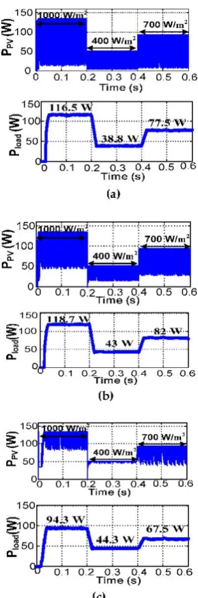
Converters are tested when PV undergoes two step-changes in irradiance from 1000 W/m2 to
400 W/m2 at 0.2 s and from 400 W/m2 to 700 W/m2 at 0.4 s. This is repeated for three different values
of input and output inductances (Li and Lo) of each converter as follows: First case; Li = Lo= 0.5 mH for Δii =20% and Δio = 40%.
Second case; Li = Lo= 1 mH for Δii =10% and Δio = 20%. Third case; Li = Lo= 5 mH for Δii =2% and Δio = 4%.
These inductances are designed according to CUK converter ripple current equation which differs in other converters as they show less ripple input current. Inductance losses are emulated by resistance connected in series to inductor and its value increases with the increase in inductance value. Switches and diodes are considered ideal. For a fair comparison, the three converters are tested for the three inductance cases with link capacitance (C) of 25 uF for Δvc = 12% and switching frequency of 15 kHz.
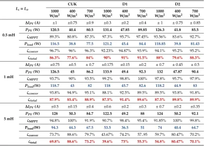
[image:15.595.86.509.170.476.2]Simulation results are shown in Figures 4–6 for CUK, D1, and D2 converters respectively. These results are analyzed, as shown in Table 3, for three different values of each converter input and output inductances (Li and Lo). It is clear that all the converters can successfully track the PV maximum power and transfer it to the load yet with different efficiencies. Increasing the input converter inductances decreases the PV power ripple which increases the average extracted PV power. Meanwhile, the inductance copper losses increase, thus decreasing the power transferred to the load. For CUK converter, its highest overall efficiency is achieved in case of 1 mH inductances. For D2, again its best overall efficiency is achieved at 1 mH while occurs at 0.5 mH in case of D1.
Figure 3.Considered system for simulation: (a) block diagram; (b)I-VandP-Vcurves of the simulated photovoltaic (PV) panel under different irradiance levels; (c) flowchart of the applied modified Inc. Cond. algorithm [9].
Converters are tested when PV undergoes two step-changes in irradiance from 1000 W/m2to 400 W/m2at 0.2 s and from 400 W/m2to 700 W/m2at 0.4 s. This is repeated for three different values of input and output inductances(Liand Lo)of each converter as follows:
First case;Li=Lo=0.5 mH for∆ii=20% and∆io=40%. Second case;Li=Lo=1 mH for∆ii=10% and∆io=20%. Third case;Li=Lo=5 mH for∆ii=2% and∆io=4%.
For CUK converter, its highest overall efficiency is achieved in case of 1 mH inductances. For D2, again its best overall efficiency is achieved at 1 mH while occurs at 0.5 mH in case of D1.
Table 3.Simulation results summary.
Li=Lo
CUK D1 D2
1000 W/m2
400 W/m2
700 W/m2
1000 W/m2
400 W/m2
700 W/m2
1000 W/m2
400 W/m2
700 W/m2
0.5 mH
∆IPV(A) ±1 ±0.75 ±0.9 ±0.3 ±0.2 ±0.4 ±1 ±0.75 ±0.85
PPV(W) 120.5 40.4 80.5 131.4 47.85 89.85 126.3 41.8 85.5
ζMPPT 89.3% 80.8% 87.3% 97.3% 95.7% 97.45% 93.56% 83.6% 92.7%
Pload(W) 116.5 38.8 77.5 121.2 45.4 84.4 118.85 39.8 81.43
ζconver 96.7% 96% 96.3% 92.23% 94.87% 93.9% 94.1% 95.2% 95.2%
ζtotal 86.3% 77.6% 84% 90% 91% 91.5% 88% 79.6% 88.3%
1 mH
∆IPV(A) ±0.75 ±0.5 ±0.7 ±0.175 ±0.15 ±0.2 ±0.7 ±0.45 ±0.5
PPV(W) 126.5 45 86.2 133.9 49.4 92.3 132 47.87 90.4
ζMPPT 93.7% 90% 93.5% 99.2% 98.8% 100% 97.8% 95.7% 97.9%
Pload(W) 118.7 43 82 118 45.7 82.6 118.2 44.9 83
ζconver 93.8% 94.9% 95.1% 88.1% 92.5% 89.5% 89.5% 93.8% 91.8%
ζtotal 87.9% 85.4% 88.9% 87.5% 91.4% 89.6% 87.5% 89.8% 89.9%
5 mH
∆IPV(A) ±0.5 ±0.15 ±0.4 ±0.6 ±0.2 ±0.3 ±0.7 ±0.2 ±0.35
PPV(W) 128 50.3 84.7 122.5 49.2 88 124 50.2 92.1
ζMPPT 94.8% 100% 91.9% 90.7% 98.4% 95.4% 91.85% 100% 99.8%
Pload(W) 94.3 44.3 67.5 53.5 36.5 51 74 40.4 64.7
ζconver 73.7% 88.6% 79.7% 43.67% 74.2% 57..95 59.7% 80.47% 70.2%
ζtotal 69.8% 88.6% 73.2% 39.6% 73% 55.3% 54.8% 80.47% 70.1%
As explained before since the input source experiences PV current and power ripples, the converters’ conversion efficiency is not the sole aspect to compare between their performance. This is vivid when comparing CUK converter performance to others at low inductances (0.5 and 1 mH). Although CUK converter shows better conversion efficiency, it transfers less power to load since it experiences higher PV power ripples (i.e., less tracking efficiency). Hence, a dominant aspect in evaluating the converters’ efficiency is the converter tracking capability to extract maximum PV power with low ripples. Thus a D1 converter with least input PV current ripples shows better overall efficiency and can transfer the highest power to load at least inductance value. However, D1 and D2 performances degrade in the case of high inductances (5 mH) due to their high copper losses. The latter decreases the load power and, meanwhile, affects the converter gain, which is directly related to the converter tracking capability resulting in low tracked PV power.
Figure 5. D1 PV power and average load power for: (a)0.5 mH; (b) 1 mH; (c) 5 mH.
Figure 5.D1 PV power and average load power for: (a) 0.5 mH; (b) 1 mH; (c) 5 mH.
Figure 6. D2 PV power and average load power for: (a) 0.5 mH; (b) 1 mH; (c) 5 mH.
In conclusion, when comparing overall efficiencies of all converters in all cases, the highest one is achieved by D1 topology applying smallest input and output inductances (0.5 mH each) which additionally, decreases system size, weight, cost and fastens system response during transients.
For deeper analysis on the converters’ efficiencies, Figure 7a focuses on the effect of converters’ inductances on tracking, conversion and overall efficiencies at a certain irradiance level (1000 W/m2).
It is clear that the tracking efficiency of D1 converter is the highest among all till 1 mH then a considerable drop occurs at 5 mH due to the high inductance losses affecting the D1 converter tracking process. However, CUK converter shows highest conversion efficiency. When combining both efficiencies, it is noticeable that the overall efficiency is greatly affected by the tracking efficiency pattern till 1 mH then it is affected by the conversion efficiency pattern. D1 converter shows highest overall efficiency at 0.5 mH while it is achieved by CUK at 5 mH. At 1 mH almost similar overall efficiency is acquired by all converters. Figure 7b shows the converters’ three efficiencies for different irradiances and in turn different power levels at the optimal inductance value (0.5 mH). It is clear that D1 converter shows the highest tracking efficiency while CUK converter acquires the highest conversion efficiency for all power levels. However, differences in conversion efficiency among the three converters are relatively very small when compared to converters’ differences in tracking efficiency. Hence, at 0.5 mH, the converters’ tracking efficiencies
Figure 6.D2 PV power and average load power for: (a) 0.5 mH; (b) 1 mH; (c) 5 mH.
Energies 2019, 12, x FOR PEER REVIEW 20 of 28
pattern has dominant effect resulting in converters’ overall efficiencies with the same pattern where the D1 converter shows the highest overall efficiency for all power levels.
40% 60% 80% 100%
0.5 1 5
Conversion Efficieny
35% 55% 75% 95%
0.5 1 5
Overall Efficiency
85% 90% 95% 100%
0.5 1 5
Tracking Efficieny
(a) (b) (c)
70% 80% 90% 100%
1000 700 400
Conversion efficiecny
70% 80% 90% 100%
1000 700 400
Tracking Efficiency
70% 80% 90% 100%
100 700 400
Overall Efficicency
[image:19.595.97.502.517.729.2](d) (e) (f)
Figure 7. Tracking, conversion and overall efficiencies of the three investigated converters for:(a–c) differentinductance values at 1000 W/m2;(d–f) variableirradiance levels at 0.5 mH.
To sum up simulation results, Figure 8 illustrates the load power achieved by the three investigated converters under three irradiance levels and for three inductances values. It is clear that at 1 mH inductances, the three converters achieve almost the same results. However, at 5 mH inductances, the highest load power is achieved by CUK, while at 0.5 mH, it is achieved by D1. Finally, among all cases, highest load power is achieved at 0.5 mH by D1 converter for the three considered irradiances levels.
Figure 8. Converters’ load power under different cases.
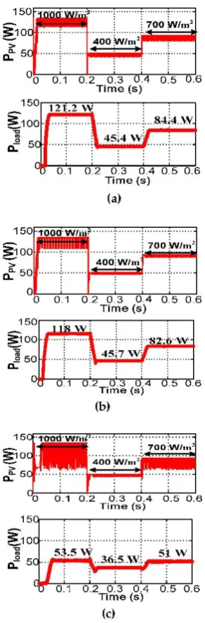
5. Experimental Results
In order to compare the performance of the considered three converters under sudden changes, a step change in irradiance is created. It is impossible to ensure similar conditions for all the investigated converters with roof-mounted PV panels, as their surrounding environmental conditions are uncontrollable. Thus, a PV module simulator can replace the actual PV panel simulating I-V and P-V curves.
A simplified PV simulating circuit is employed, as shown in Figure 9a [9,29]. This circuit emulates the PV source when exposed to sudden step-change in irradiance. It consists of a DC power supply with constant voltage of 30 V and two parallel resistances of 6.667 Ω each to represent Rss. When the switch S is on, the two resistances are in parallel and Rss is about 3.5 Ω and
Energies2019,12, 2208 20 of 27
To sum up simulation results, Figure8illustrates the load power achieved by the three investigated converters under three irradiance levels and for three inductances values. It is clear that at 1 mH inductances, the three converters achieve almost the same results. However, at 5 mH inductances, the highest load power is achieved by CUK, while at 0.5 mH, it is achieved by D1. Finally, among all cases, highest load power is achieved at 0.5 mH by D1 converter for the three considered irradiances levels. pattern has dominant effect resulting in converters’ overall efficiencies with the same pattern where the D1 converter shows the highest overall efficiency for all power levels.
40% 60% 80% 100%
0.5 1 5
Conversion Efficieny
35% 55% 75% 95%
0.5 1 5
Overall Efficiency
85% 90% 95% 100%
0.5 1 5
Tracking Efficieny
(a) (b) (c)
70% 80% 90% 100%
1000 700 400
Conversion efficiecny
70% 80% 90% 100%
1000 700 400
Tracking Efficiency
70% 80% 90% 100%
100 700 400
Overall Efficicency
(d) (e) (f)
Figure 7. Tracking, conversion and overall efficiencies of the three investigated converters for:(a–c) differentinductance values at 1000 W/m2;(d–f) variableirradiance levels at 0.5 mH.
To sum up simulation results, Figure 8 illustrates the load power achieved by the three investigated converters under three irradiance levels and for three inductances values. It is clear that at 1 mH inductances, the three converters achieve almost the same results. However, at 5 mH inductances, the highest load power is achieved by CUK, while at 0.5 mH, it is achieved by D1. Finally, among all cases, highest load power is achieved at 0.5 mH by D1 converter for the three considered irradiances levels.
Figure 8. Converters’ load power under different cases.
5. Experimental Results
In order to compare the performance of the considered three converters under sudden changes, a step change in irradiance is created. It is impossible to ensure similar conditions for all the investigated converters with roof-mounted PV panels, as their surrounding environmental conditions are uncontrollable. Thus, a PV module simulator can replace the actual PV panel simulating I-V and P-V curves.
[image:20.595.189.409.173.308.2]A simplified PV simulating circuit is employed, as shown in Figure 9a [9,29]. This circuit emulates the PV source when exposed to sudden step-change in irradiance. It consists of a DC power supply with constant voltage of 30 V and two parallel resistances of 6.667 Ω each to represent Rss. When the switch S is on, the two resistances are in parallel and Rss is about 3.5 Ω and
Figure 8.Converters’ load power under different cases.
5. Experimental Results
In order to compare the performance of the considered three converters under sudden changes, a step change in irradiance is created. It is impossible to ensure similar conditions for all the investigated converters with roof-mounted PV panels, as their surrounding environmental conditions are uncontrollable. Thus, a PV module simulator can replace the actual PV panel simulatingI-VandP-Vcurves.
A simplified PV simulating circuit is employed, as shown in Figure9a [9,29]. This circuit emulates the PV source when exposed to sudden step-change in irradiance. It consists of a DC power supply with constant voltage of 30 V and two parallel resistances of 6.667Ωeach to representRss. When the switch S is on, the two resistances are in parallel andRssis about 3.5Ωand this gives aP-Vcurve of almost 64.3 W peak power. When S is opened,Rssbecomes 6.667Ωresulting in a step decrease in the currentIproducing a differentP-Vcurve with reduced peak power level (33.75 W) as shown in Figure9b. Figure9c shows the test rig photograph of the considered system.
Each of the three considered buck-boost converters is implemented and its performance is tested at 15 kHz switching frequency and under step change in power level (from 33.75 W to 64.3 W). This is repeated for three values of converters’ input and output inductances (0.7, 1.4, and 2.8 mH).
[image:20.595.94.501.617.692.2]Experimental results of the considered converters are analyzed in all cases, and their tracked PV power and average load power values are computed and compared in Figure10while the converters’ overall efficiencies are computed in Table4.
Table 4.Experimental converters’ overall efficiencies.
Li=Lo
CUK (C3) D1 D2
Low Power High Power Low Power High Power Low Power High Power
0.7 mH ζtotal 73.8% 82.3% 83.5% 82.9% 78% 79.2%
1.4 mH ζtotal 75.6% 81.5% 80 % 77% 76. 7% 77.4%
2.8 mH ζtotal 54.2 % 57.4% 37. 3% 37.6% 42.4% 45.7%
Energies2019,12, 2208 21 of 27
(a) (b)
(c)
Figure 9. Experimental setup:(a) schematic diagram; (b) test rig photography, (c) PV emulator P-V, I-V curves.
[image:21.595.90.505.93.390.2]Each of the three considered buck-boost converters is implemented and its performance is tested at 15 kHz switching frequency and under step change in power level (from 33.75 W to 64.3 W). This is repeated for three values of converters’ input and output inductances (0.7, 1.4, and 2.8 mH).
Table 4. Experimental converters’ overall efficiencies.
Li=Lo
CUK (C3) D1 D2
Low Power High Power Low Power High Power Low Power High Power
0.7 mH ζtotal 73.8% 82.3% 83.5% 82.9% 78% 79.2%
1.4 mH ζtotal 75.6% 81.5% 80 % 77% 76. 7% 77.4%
2.8 mH ζtotal 54.2 % 57.4% 37. 3% 37.6% 42.4% 45.7%
Experimental results of the considered converters are analyzed in all cases, and their tracked PV power and average load power values are computed and compared in Figure 10 while the converters’ overall efficiencies are computed in Table 4.
It is clear from Figure 10 that the three converters can successfully track the PV power during sudden changes, and reasonably transfer the tracked power to the load yet with different levels of accuracy and efficiency. A noticeable decrease in load power occurs at 2.8 mH for all converters due to high inductance losses, yet CUK converter shows higher load power in this case for its higher conversion efficiency.
Figure 9.Experimental setup: (a) schematic diagram; (b) test rig photography, (c) PV emulatorP-V,
I-VEnergies curves.2019, 12, x FOR PEER REVIEW 22 of 28
(a)
(b)
Figure 10. Experimental results analysis: (a) PV power; (b) average load power.
However, among all cases of converters’ inductance values, the D1 converter shows the highest PV tracked power and highest load power, during various power levels, at the lowest inductance value (0.7 mH) and in-turn highest overall efficiency, as shown in Table 4. This is related to the D1 converter’s inherited feature of minimal PV power ripples and highest tracking efficiency, as shown in Figure 11a, resulting in highest tracked PV power and in turn highest load power as clarified in Figure 11b.
Hence, experimental results verify those of the simulation confirming that the converter tracking efficiency has a dominant effect on the converter’s overall efficiency, thus the D1 converter shows highest load power at low size input and output inductances.
[image:21.595.144.452.434.749.2]However, among all cases of converters’ inductance values, the D1 converter shows the highest PV tracked power and highest load power, during various power levels, at the lowest inductance value (0.7 mH) and in-turn highest overall efficiency, as shown in Table4. This is related to the D1 converter’s inherited feature of minimal PV power ripples and highest tracking efficiency, as shown in Figure11a, resulting in highest tracked PV power and in turn highest load power as clarified in Figure11b.
Hence, experimental results verify those of the simulation confirming that the converter tracking efficiency has a dominant effect on the converter’s overall efficiency, thus the D1 converter shows highest load power at low size input and output inductances.Energies 2019, 12, x FOR PEER REVIEW 23 of 28
Figure 11. Experimental results of CUK, D1 and D2 converters at 0.7 mH: (a) PV power; (b) average load power.
6. Discussion
In this subsection, three critical issues need to be clarified to avoid readers’ confusion.
6.1. Why are the Inductance Values Used in the Simulation Different than those Used in the Experimental Verification?
Utilizing the PV emulator is unavoidable and cannot be replaced by a PV panel to ensure consistency of the environmental operating conditions as the main article concern is the performance evaluation of three DC/DC converters.
From the authors’ point of view, the experimental setup should in these circumstances specifically utilizes parameters differ than that of the simulation for the following reasons:
1. The different range of examined PV power, input and output DC voltage at the converter terminals, input and output current across the examined converter, percentage acceptable ripples in the system currents, etc… are all aspects characterizing the fact that both the simulation and experimental analysis are different and hence mandate the utilization of different converter inductances in the experimental setup in order to ensure the CCM and preserve the same acceptable power and current oscillation level. This is in order to achieve fair counterpart DC/DC converters performance assessment as the main factor in selecting the inductor values to ensure CCM is the percentage current ripples which is not the same as in simulation due to the difference in system aspects as mentioned above. The inductance values are selected just above the minimum value that ensure the CCM operation to avoid the added conduction loss that may be exerted when higher values of inductances are selected as their parasitic resistance is proportional to the inductance values.
[image:22.595.91.509.209.462.2]2. Comparative analysis between counterparts can be enhanced by using system parameters in the simulation that differ from that in the experimental assessment. The simulation assessment examines the investigated converters using certain inductance values and operating condition where a conclusion is deducted from this assessment. The authors perform the experimental analysis with different system parameters to emphasise that the conclusions obtained from the
Figure 11.Experimental results of CUK, D1 and D2 converters at 0.7 mH: (a) PV power; (b) average load power.
6. Discussion
In this subsection, three critical issues need to be clarified to avoid readers’ confusion.
6.1. Why are the Inductance Values Used in the Simulation Different than those Used in the Experimental Verification?
Utilizing the PV emulator is unavoidable and cannot be replaced by a PV panel to ensure consistency of the environmental operating conditions as the main article concern is the performance evaluation of three DC/DC converters.
From the authors’ point of view, the experimental setup should in these circumstances specifically utilizes parameters differ than that of the simulation for the following reasons:
in system aspects as mentioned above. The inductance values are selected just above the minimum value that ensure the CCM operation to avoid the added conduction loss that may be exerted when higher values of inductances are selected as their parasitic resistance is proportional to the inductance values.
2. Comparative analysis between counterparts can be enhanced by using system parameters in the simulation that differ from that in the experimental assessment. The simulation assessment examines the investigated converters using certain inductance values and operating condition where a conclusion is deducted from this assessment. The authors perform the experimental analysis with different system parameters to emphasise that the conclusions obtained from the simulation results are still valid even if the system power, voltage/current level, oscillation percentage change. Consequently, the final conclusions are mainly converters’ trend and irrelevant to the selected inductance values. From the authors’ point of view, this way of assessment adds elaborated generalization of the obtained results emphasizing on their uniqueness irrespective from the designer selection of the converter inductances.
6.2. Why are the Investigated Converters Examined at 15 kHz, a Relatively Low Switching Frequency?
The authors prefer to perform the converters assessment at this low switching frequency as this reflects the worst case scenario where the converter loss is comparable with the power loss due to the divergence in the tracking efficiency. Hence, from the authors’ point of view this range of operations is the most confusing to designer selection as the converters’ performance might appear similar if only the conversion efficiency is considered. Hence, adequate assessment incorporating the tracking efficiency is unavoidable.
Technically, the majority of the installed PV systems adopt either central or string converter configuration featuring medium to high power scale converters. These converters by nature utilize low-order switching frequencies (several kHz range) to minimize the massive switching loss that evolve rapidly when the converter switching frequency increases. Hence, the paper focuses its research towards this range of widespread PV converters. The high switching frequency is adopted by low power (up to 300 W) PV converters named AC modules/micro-inverters that acquire a small share in the PV converters’ commercial market, hence being less important to address at this stage.
6.3. Does the Photovoltaic (PV) Generator Affect the Interfacing Converter Dynamics?
Voltage-type sources have dominated as an input source for power electronics converters for a long type. The existence of duality implies that there are also current-type sources. The growing application of renewable energy sources such as wind and solar energy has evidently shown that the current-type input sources exist in reality such as a PV generator or the feedback technique used in controlling the power electronics converters in the renewable energy systems changes the power electronic converters to behaving in this way. Recent research on renewable energy systems has indicated that the current-type input sources are very challenging input sources affecting the dynamics of the interfacing converters profoundly.The dual nature of the PV generator (i.e., the constant-current region (CCR) at the voltage less than the maximum-power-point (MPP) voltage, and the constant-voltage region (CVR) at the voltages higher than the MPP voltage) [12] may imply that the PV non-linear nature heavily influence the interfacing converter dynamics as it cannot be considered as a simple DC voltage source.
the operating point [34], and the change of sign of the control-to-output transfer function, when the operating point travels through the MPP [35]. In some cases, the RHP zero can be removed by the design of the converter power stage as explained in [36], but usually the RHP zero will effectively limit the output-side feedback-loop control bandwidth to rather low frequencies [37].
Consequently, a detailed analysis is unavoidable considering the dynamic PV generator model when a closed loop control system is to be designed. This issue needs more attention especially if the utilized converter will be used in two stage grid feeding/grid forming conversion system. The stability aspect mandates deep analysis of the source-converter dynamic modelling to avoid/manipulate RHP zero creation. The authors clarify that the RES–converter interface, specially when the RES exhibits non-linear nature, must be carefully analyzed. The utilization of the PV system in this paper was for illustration purpose only for the newly addresses aspect, the tracking efficiency. Hence, a converter interfacing an RES was unavoidable. But, the stability and controller design aspects related to the interface of PV non-linear model on the converter dynamics is out of scope of the present manuscript.
7. Conclusions
The paper presents a detailed comparison for three continuous-input/continuous-output current DC/DC converters. Dynamic modeling and small signal analysis of two continuous-input continuous-output current buck-boost converters (D1 and D2) are derived and compared to those of a CUK converter when operated in voltage-fed-mode. Although the CUK converter has the least converter losses, D1 converter was found to have the least input current ripples. The latter greatly affects the converter overall efficiency when if applied as RES interfacing converter as it enhances the MPPT process and maximizes the extracted output power. The converters’ performances are assessed, using simulation and experimental results, when being applied to a PV stand-alone system, as an example, under varying irradiance for three different values of converters’ inductances. Among all cases, the D1 converter transfers the highest power to the load and achieves the most enhanced total efficiency at small size inductances which in turn decreases system weight and cost.
Author Contributions: Conceptualization, A.K.A.; Formal analysis, N.E.Z. and A.K.H.; Investigation, N.E.Z.; Methodology, N.E.Z. and A.K.A.; Project administration, B.W.W.; Supervision, B.W.W.; Validation, A.K.H.; Writing–original draft, N.E.Z.; Writing–review & editing, A.K.A.
Funding:This research receives no external funding.
Conflicts of Interest:The authors declare no conflict of interest.
List of Symbols
Co Converter output capacitor RLi Resistance of converter intput inductor
D Switch duty ratio RLo Resistance of converter output inductor
D’ 1- D T Converter switching period
fsw Converter switching frequency vi Converter input voltage
ic Capacitor current vo Converter output voltage
id Diode current vS Switch voltage
ii Converter input current vc Capacitor voltage
io Converter input current vLi Voltage of converter input inductor
iLi Current of converter input inductor vLo Voltage of converter output inductor
iLo Current of converter output inductor ZC Impedance of converter link capacitor
Li Converter input inductance ZLi Impedance of converter input inductor
Lo Converter output inductance ZLo Impedance of converter output inductor
Pload Load power Zo Converter output impedance
PPV Tracked PV power X Average value of the specified quantity
M Converter conversion ratio ∆x Ripples of the specified quantity