This is a repository copy of Theory of direct and indirect effect of two-photon absorption on nonlinear optical losses in high power semiconductor lasers.
White Rose Research Online URL for this paper: http://eprints.whiterose.ac.uk/113942/
Version: Accepted Version Article:
Avrutin, E. A. orcid.org/0000-0001-5488-3222 and Ryvkin, B. S. (2017) Theory of direct and indirect effect of two-photon absorption on nonlinear optical losses in high power semiconductor lasers. Semiconductor science and technology. 015004. ISSN 0268-1242 https://doi.org/10.1088/1361-6641/32/1/015004
[email protected] https://eprints.whiterose.ac.uk/
Reuse
Items deposited in White Rose Research Online are protected by copyright, with all rights reserved unless indicated otherwise. They may be downloaded and/or printed for private study, or other acts as permitted by national copyright laws. The publisher or other rights holders may allow further reproduction and re-use of the full text version. This is indicated by the licence information on the White Rose Research Online record for the item.
Takedown
If you consider content in White Rose Research Online to be in breach of UK law, please notify us by
- 1 -
Theory of direct and indirect effect of two photon absorption
on nonlinear optical losses in high power semiconductor laser
E.A.Avrutin1 and B.S. Ryvkin2,3.
1
Dept of Electronics, University of York, York YO10 4LE, UK 2
A.F.Ioffe Physico-Technical Institute, St.Petersburg 194021, Russia 3
ITMO University, St.Petersburg 197101, Russia
Abstract: the effect of the transverse laser structure on two-photon absorption (TPA) related
effects in high-power diode lasers is analysed theoretically. The direct effect of TPA is found to
depend significantly on the transverse waveguide structure, and predicted to be weaker in broad and
asymmetric waveguide designs. The indirect effect of TPA, via carrier generation in the waveguide
and free-carrier absorption, is analysed for the case of a symmetric laser waveguide and shown to
be strongly dependent on the active layer position. With the active layer near the mode peak, the
indirect effect is weaker than the direct effect due to the population of TPA-created carriers’ being
efficiently depleted by their diffusion and capture into the active layer, whereas for the active layer
position strongly shifted towards the p-cladding, the indirect effect can become the dominant power
limitation at very high currents. It is shown that for optimizing a laser design for pulsed high power
operation, both TPA related effects and the inhomogeneous carrier accumulation in the waveguide
- 2 -
Introduction.
High power semiconductor lasers find numerous applications including, but not restricted to, optical
communications (e.g. solid state laser and amplifier pumping), manufacturing industry, metrology
and spectroscopy, optical radars, etc. (see e.g. [1] [2] for an overview). Achieving high output
power and high efficiency is of paramount importance for many of these applications; this requires
optimizing the laser structure, which in turn needs detailed understanding of physical phenomena
that affect the laser performance at high power operation.
Since high-power diode lasers typically operate very high above threshold, the most important
parameters for achieving high power output are the slope and injection efficiency of the laser, which
need to be maximized. High slope efficiency, in its turn, requires low internal parasitic losses. All
high-power lasers currently in use comprise a relatively broad Optical Confimenent Layer (OCL),
sandwiched between p- and n- claddings and containing within it a thin (single or two-three
Quantum Wells) Active Layer (AL). Then, the low parasitic losses at low to moderate pumping
currents are ensured primarily by reducing the overlap of the transverse laser mode of the laser
waveguide with the lossy p-cladding. A number of laser designs have been proposed to achieve
this. Historically the first, and still the most widespread at the moment, is the design including a
broadened (OCL thickness h > 1.5-2 m), waveguide, symmetric or approximately symmetric in the
sense that it has equal or similar refractive index steps at the boundaries between the OCL and both
claddings; see for example [3-8]. The AL can be positioned either at or near the centre of the OCL
as in [3-8], or near the p-cladding as in the case of Slab Coupled Optical Waveguide Lasers
(SCOWL; see e.g. [9]). The broad OCL and a substantial refractive index step at the
OCL-p-cladding interface ensure that most of the transverse mode power is contained within the OCL
rather than the claddings, making for low internal losses, at least at low to moderate currents. The
- 3 -
authors, e.g. [2], [10] [11] [12], builds partly on the earlier ideas of [13] and involves a substantially
asymmetric waveguide with a refractive index step between the n-cladding and the OCL
substantially smaller than that between the OCL and the p-cladding. Depending on the OCL
thickness and the exact value of the refractive index steps, such a waveguide can be broad (in the
sense that most of the optical power of the mode is localized in the OCL) or narrow (in the sense
that most of the mode resides in the n-cladding [14]), but in either case the overlap with the
p-cladding is kept low, ensuring low p-cladding-related optical loss. Recently, it was the broader
asymmetric waveguide that found extensive use for both steady state operated [2] and
gain-switched [10, 15] lasers.
It follows from our semi-analytical calculations [16],[17] and has been confirmed numerically and
experimentally [2] that a structure with a strongly asymmetric position of the active layer (very
near to the p-cladding) can be expected to keep its low-loss advantage, not just at low to moderate
operating currents, but at high currents too. This is because such a structure minimizes the effect of
spatially inhomogeneous accumulation of carriers in the OCL (mainly the p-side of it) at high
currents due to the finite time of ambipolar-type carrier diffusion from the claddings across the
OCL to the AL, and hence the free-carrier and intervalence band absorption by the carriers thus
accumulated. Since the characteristic carrier density, which scales the optical loss, is in this case
approximately proportional to the thickness of the p-OCL (the fraction of the OCL between the
active layer and the p-cladding), this source of nonlinear loss is particularly efficiently minimized in
laser designs with the position of the active layer shifted from the mode peak towards the
p-cladding, particularly ones where the refractive index profile is also asymmetric [2, 11, 12] (the
- 4 -
However, some sources of nonlinear loss at high currents clearly exist in any high-power laser
design, symmetric or asymmetric, since even EDAS structures have been shown to exhibit power
saturation at high currents, albeit at somewhat higher powers than symmetric structures [2] [12].
Several nonlinear mechanisms of such loss have been identified. Firstly, there is the relatively well
known effect of free carrier absorption by the homogeneously distributed carrier population
accumulated in the OCL due to the nonzero time of their capture from the OCL to the active layer
and the nonzero rate of their thermal escape in the opposite direction [3] [18] [19]. Secondly,
recently, it has been pointed out that given the high light intensities, the Two-Photon Absorption
(TPA) within the waveguide, originally investigated for semiconductor optical amplifiers [20] [21],
may become important in high-power lasers [22] [23].
The TPA effect, in its turn, involves in fact two effects: (i) the direct effect of nonlinear loss due to
TPA and (ii) the indirect effect of the TPA serving as yet another source of carrier accumulation in
the waveguide (OCL and claddings), adding to the optical losses due to free-carrier and intervalence
band absorption. In [22], the indirect effect of the TPA was estimated as being, at least in some
cases, more important than the direct one. The authors achieved good agreement with experiments
for one particular, broad symmetric waveguide, laser design, using the bulk values of the
Two-Photon Absorption, postulating a recombination time for the TPA-created free carriers in the OCL
of the order of 10 ns (typical for nonradiative and spontaneous recombination in a weakly doped
layer), and neglecting all other high-power loss mechanisms. The question of carrier transport, and
therefore of the carrier distribution across the OCL, was not considered in those papers. It is
therefore of interest to address the issue of the direct and indirect effects of the TPA for different
waveguide structures (with transport taken fully into account), their relative importance compared
to other loss mechanisms and to each other, and their dependence on the laser design. This is the
- 5 -
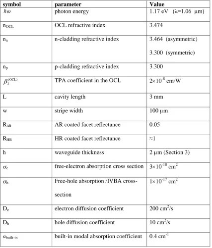
1. The laser designs considered.
We shall consider here representative examples of both of the main high-power laser designs
discussed above. The first is a broadened, symmetric waveguide structure, intended for operation at
=1.06 m. The prototype version of the structure, shown in Figure 1a (solid line) alongside the
corresponding modal power distribution, is a broad symmetric waveguide with h=2 m and the AL
positioned near the centre (slightly shifted towards the p-cladding to aid higher order mode
discrimination [5] [24]); however in the simulations, both the OCL thickness and the AL position
(the extreme case of the AL located near the OCL/p-cladding interface being shown in a dashed line
as case 2 in Figure 1a) could be varied.
For comparison, we also consider a (broad) asymmetric structure, with the refractive index contrast
at the OCL/n-cladding interface reduced to 0.01 and that at the OCL/p-cladding interface kept the
same as in the symmetric structure. Shown in Figure 1b is the case of h=2 m as in Figure 1b,
though in simulations, again, an arbitrary thickness was considered. The main calculation
parameters and their values are listed in Table 1.
2. The direct TPA effect.
The local two-photon absorption at any point in the laser waveguide can be written as
TPA( , )x z
2( ) ( , ),x J x z (1)with 2( )x [cm/W] the two-photon absorption coefficient, characterised by a (relatively weak)
dependence on the transverse (vertical) coordinate x because of its dependence on the material
- 6 - evaluated as J x z( , ) P z( ) 2( ).x
w
Here P(z) is the power at a given longitudinal position z, w is the
laser stripe width (assuming a broad area laser, we consider the light distribution homogeneous in
the lateral coordinate; a 2D generalisation for a single-mode stripe waveguide, along the lines
presented in [21], is straightforward ), and 2 ( )x
is the laser modal intensity profile as shown in
Figure 1 (( )x being the modal electric field distribution), normalised so that that 2( )x dx 1
.The modal TPA coefficient can then be calculated in the usual fashion of calculating waveguide
absorption: TPA(mod)( )z TPA( , )x z2( )x dx
, giving(mod) 4
2 1
( ) ( ) ( ) ( );
TPA z x x dx P z
w
The calculation may be further simplified by noting that the dependence of the TPA coefficient on
the refractive index step in the waveguide is of relatively little importance for both structures of
interest: in the symmetric structure (and to a lesser extent in the asymmetric one as well), this is
because of the relatively weak penetration of the field into the claddings for all important h values,
and in the asymmetric structure, also because the composition, and thus the value of 2( )x , in the
OCL and the n-cladding (which between them contain nearly all the mode intensity) are very
similar. Then, we can evaluate the TPA using the very simple formula
( )
(mod) 2 4 ( )
2 ( ) ; OCL OCL TPA TPA P x dx P
w h w
(2)Here, ( ) 2
OCL
is the TPA coefficient of the OCL (GaAs in our case) at the operating wavelength of
- 7 -
1 4
( ) TPA
h x dx
is the transverse dimension characterising TPA in the waveguide. Eq. (2) is essentially a
broad-area device version of the 2D integral given in [21].
Since in the waveguide structures of Figure 1, the effect of the active layer on the waveguiding is
very weak, we can use the standard expression (see e.g. [25]) for the modal profile ( )x in a
three-layer slab waveguide
0 1
( )x cos( x ) C
, 0<x<h (OCL) (3)a
0 1
( )x cos exp( nx) C
, x<0 (n-cladding) (3b)
0 1
( )x cos( h ) exp p(x h) C
, x> h (p-cladding) (3c)
where 2 nOCL2 n02
is the transverse wave vector of the waveguide mode in the OCL,
2 2 0 2
n n nn
and p 2 n02 n2p
are the decrements of decay into the n- and p-claddings,
and arctan n
. The values of ,n, and pare calculated from the effective refractive
index n0 of the fundamental (TE) mode and the refractive indices nOCL, np, nn of the OCL, p- and
n-cladding layers, respectively; see Appendix 1 for more detail. The normalisation constant is
calculated as
2 eff o
h
C , where eff 1 1
n p
h h
- 8 -
characterises the transverse spread of the mode; for a mode well contained within the OCL, heff≈h.
The magnitude heff/2 is the effective mode size, defined (see e.g. [22]) as the width of a “top-hat”
profile that contains the same total energy as the modal distribution 2( )x given the same
amplitude 2peak. For a thin (da< < h) active layer located at the peak of the mode, heff/2 also
coincides with the ratio da/ ( a 2( )l da abeing the confinement factor, or the overlap of 2
( )x
with the active layer located at x= la ), which is sometimes termed the equivalent spot size of the
mode.
The formulas (3)a-c for ( )x allow an explicit, if somewhat cumbersome, expression (A1.7) to be
obtained for
1 4
( ) TPA
h x dx
; see Appendix 1.The result, obviously, depends on the specific design of a waveguide: nOCL, np, nn, and h.
Given a certain effective mode size heff/2, simple universal (not tied to a particular waveguide
design) approximations for ( )x can be constructed in order to obtain approximate estimates of
waveguide properties, including the TPA parameter hTPA . The first of these is a top-hat profile with
an amplitude of 1 /C0 2 /heff and thus a width of heff/2, which gives an estimate
( )
/ 2 top hat
TPA eff
h h . The second (a one-dimensional equivalent of a two-dimensional approximation
used in [21] for a narrow stripe waveguide with a single transverse and lateral mode) is a Gaussian
profile with the same amplitude (which, given the normalisation 2( )x dx 1
, ensures the same- 9 -
Shown in Figure 2, as functions of h, are the values of the integral 4( )x dx 1/hTPA
,which scalesthe absorption coefficient TPA(mod), for the symmetric (a) and asymmetric (b) waveguide designs,
calculated both accurately and using the top-hat and, in the case of a symmetric waveguide,
Gaussian approximations for the same heff. It is seen from the figure that, whilst for narrow
waveguides the accurate evaluation is desirable, for broader ones (in excess of about a micrometer),
the Gaussian approximation gives a very accurate estimate.
Interestingly, the TPA in a broad symmetric waveguide (with a typical value of h~2 m) can be
expected to be significantly greater than in an asymmetric waveguide at the same power and with a
similar waveguide thickness, because the asymmetric waveguide mode has a larger effective size.
We note that a formalism equivalent but alternative to Eq. (2), used in [21] and [22] to describe the
TPA in a laser or amplifier, is to introduce the effective modal light intensity, or flux, Jmod, and
express the nonlinear loss coefficient in a form formally identical to the bulk expression (1):
(mod) (mod) 2 mod ( )
TPA z J
, with an effective modal TPA coefficient (mod) 2
. However, in this case ne
needs to take some care about the way the effective flux, and thus the effective modal TPA
coefficient, are defined. Using only the waveguide mode parameters, Jmod can be defined as
Jmod=P/Amod as in [21], where Amod is the effective modal cross-section (in the case of a broad-area
slab waveguide, Amod=heffw/2 in our notations; the two-dimensional generalisation for a
single-mode stripe waveguide is given in [21]). With such notations, from (2), 2(mod) 2( ) / (2 ) OCL
eff TPA
h h
,
and in the Gaussian approximation, which, as mentioned above, is very accurate for broad
symmetric waveguides, simply 2(mod) 22(OCL)/ 2. The authors of [22] used a different,
generally speaking, definition of the effective modal flux, performing their calculations, instead of
- 10 - the stimulated recombination rate a a
stim
dN J
g
dt
of carriers in the AL (g being the gain and Na,
the AL carrier density). Note that Ja= Jmod if and only if the AL is located at the mode peak. In
terms of the flux Ja, one can express the absorption coefficient formally as TPA(mod) 2(mod,a)Ja, where
the equivalent modal TPA coefficient is calculated as 2(mod,a)2(OCL)da / (2a TPAh ) and is thus,
generally speaking, a function of the AL position, even though the actual absorption (mod) TPA
is not, if
da< < h. In [22], an approximation TPA(mod) 2(OCL)Ja was used; without knowing the waveguide
structure and the position of the OCL in the waveguide used in [22], one cannot compare this
approximation with the more accurate calculation using (mod,a) 2
. We believe the expression (2) is
thus the most straightforward and unambiguous representation of the nonlinear properties of a laser
waveguide, since it relates the nonlinear absorption to local power, a parameter independent on the
modal structure.
3. The indirect TPA effect: TPA-created carriers.
The TPA-created carriers are generated throughout the OCL and removed, firstly, through radiative
and nonradiative recombination, and, secondly, through transport and subsequent capture into the
active layer. In analysing the transport, we follow the previous work [16, 17, 26] in assuming
detailed quasineutrality. In an undoped or very weakly doped OCL considered here, this means
identical electron and hole densities Ne≈Nh≈N throughout the bulk of the OCL (that is, in the whole
of the OCL with the exception of a narrow region around the active layer). The approximation is in
excellent agreement with numerical simulations in the absence of TPA, and can be confidently
expected to hold in its presence as well, seeing that TPA creates electron-hole pairs at each point.
Note that the second of the approximations made in [16, 17, 26], that of the absence of the electron
current in the entire p-OCL (which is defined as the area la<x<h) and the hole current in the entire
- 11 -
and/or recombination. With quasineutrality postulated, the carrier transport is described by the
standard ambipolar diffusion equation (including z dependence because of the variation of power
along the resonator length):
2
2 ( , ) ( ( , )) 0 a
N
D G x z R N x z
x
(4)
Here, 2 e h a
e h D D D
D D
is the ambipolar diffusion coefficient, De and Dh being the electron and hole
diffusion coefficients in the OCL material, diffusion in the longitudinal direction z is omitted due to
the relatively long distance scales involved, and the generation term is given by the TPA rate:
2 4 2( ) ( )
( , ) x P z ( )
G x z x
w
(5)
The recombination rate R should, in principle, include both the bimolecular radiative and linear
nonradiative recombination terms as in [26]. However, as was shown previously [26], in the
absence of TPA the recombination term is only important with very high (in excess of 1018 cm-3)
OCL carrier densities and/or very broad OCL (~3-4 m). Here we consider somewhat narrower
OCLs, and are primarily concerned with GaAs/AlGaAs materials where Da is a few times greater
than in InGaAsP quaternaries treated in [26], so it can be confidently expected that with TPA
present, transport and subsequent capture should remain a more efficient OCL carrier dissipation
route than recombination. Therefore in this paper we shall only consider transport, not
recombination, and set R=0 in the first approximation. If necessary, it is relatively straightforward
to include recombination in the second approximation using an approximate iterative procedure [26]
having first calculated the carrier distribution with R=0; linear recombination could even be
included exactly from the start but is unlikely to be the dominating recombination mechanism due
- 12 -
The boundary conditions for Eq. (4) are taken to be approximately the same as in the absence of
TPA[16, 17, 26] : at the interfaces with injectors (claddings), the current is carried almost entirely
(entirely, barring current leakage) by electrons at the OCL-n-cladding interface x=0 and by holes at
the OCL-p-cladding interface x= h :
0
; ;
2 2
lh le
x e x h h
j j
N N
x D x D
(6)
Here,
lh
lh( )j and
le le( )j are efficiency coefficients describing the leakage of hole currentinto the n-cladding and of electron current into the p-cladding correspondingly; they can be
estimated as described in [18] [27] and are equal to one in the absence of leakage. Note that the
analysis below is restricted to situations when the leakage is not strong ( lh, le are close to one)
which is nearly all situations of practical interest in GaAs/AlGaAs lasers, particularly for the
strongly guiding structure of Figure 1a.
At the OCL (more accurately, at a very small distance away from it, where the bulk quasineutrality
begins to hold, but this distance is much smaller than h so can be neglected), we have
a a b
x l x l
N N N (7)
, where Nb is the background carrier density determined by the balance of carrier capture from the
OCL into the AL and the thermally activated escape in the opposite direction, as in previous papers.
Strictly speaking, both boundary conditions are slightly affected by the presence of the TPA: the
conditions (6) because
lh and
leare affected by the TPA in the claddings themselves, and theconditions (7) because TPA adds some extra carriers to the balance of capture and escape –
however both effects can be estimated to be rather weak.
In the absence of bimolecular recombination, Eq. (4) is linear in N, so its solution with the boundary
- 13 -
including the spatially homogeneous background Nb and the spatially inhomogeneous part Nj(x)
caused only by current flow and identical in its form to the results of [17] [16], and secondly, the
TPA-dependent part NTPA(x,z) proportional to P2:
( , ) b j( ) TPA( , ) N x z N N x N x z
(8)
With R=0, the current contribution is the same as derived in [16, 17, 26]:
( ) ; 0
2
( ) ;
2 lh
j a a
e
le
j a a
h j
N x l x x l
D
j
N x x l l x h
D
(9)The spatially homogeneous background Nb can be estimated as
b cap bT
a j N N ed
(10)where cap is the characteristic time of carrier capture into the QW AL which for the carrier density values small enough to keep the quasi Fermi levels deep in the well has been calculated (see e.g.
[28]) as cap~ (100-200) fs; da is the AL thickness (taken as 10 nm). The term N describes the bT thermal escape from the AL into the OCL. Under room temperature operation, which is the subject
of this paper, it is usually weak, but can easily become dominant at elevated temperatures which
are characteristic of true CW high power operation.
The TPA-generated carrier density is obtained by integrating the generation term (5) twice with the
boundary conditions 0
0; 0
a a
TPA TPA
TPAx l TPAx l
x x h
N N
N N
x x
The integration itself is trivial if somewhat cumbersome; the explicit resulting expressions are
- 14 -
From the carrier distributions, since both the carrier density accumulation and the waveguide mode
in the laser structures are localised in the OCL (as illustrated in Figure 3) under the conditions
considered here, the corresponding contributions to the internal absorption are calculated as
( ) 2
0
( ) , ( )
h FC
j z e h Nb NbT Nj x z x dx
(11)
and
( ) 2
0
( ) , ( )
h FC
TPA z e h NTPA x z x dx
,(12)
where e, h are the free-electron and free-hole absorption cross-sections, respectively.
Note that in (11), we have included the contributions from both Nj and the current-dependent part
of Nb since both are scaled by the current density j.
The relative magnitudes of Nj and NTPA are somewhat current dependent since Nj is
proportional to the current density j and NTPA, as already noted in [22] [23], to the square of
power and hence depends on j superlinearly, if not exactly quadratically, therefore its relative effect
compared to Njincreases with current.
To calculate the power P(j) needed for evaluation of NTPA, we used a self-consistent procedure
including all the nonlinear loss mechanisms discussed here. Within this procedure, the power P as
function of current i (or current density j= i/wL, recalculated using the cavity length L=3 mm, width
w=100 µm) is determined from a transcendental equation
( )
( , ( ))out
th out in
P i i i
e i P i
(13)
where the output loss 1 ln 1 2
out
HR AR
L R R
was calculated assuming the high-reflectance and
- 15 -
affect the results much, given the range of currents i> > ith. The internal loss was calculated as a
sum of all contributions
in( , ( ))i P i
in(built in)
(FC)j ( )i
TPA(FC)( ( ))P i
TPA(mod)( ( ))P i (14)
In this equation, the constant built-in absorption in(built in) included the effects of cladding doping,
structure imperfections, and free carrier absorption by the thermally escaping OCL carriers (the
NbT term in (10)); the value for it was taken as 0.4 cm-1 [24]. We treat the case of pulsed
(quasi-CW) operation so the thermal roll-over is not considered in the simulations, and the value of NbT
can be approximately taken as constant. For the free-carrier absorption cross-sections, we used
e=310-18 cm2, h=110-17 cm2 as in previous work [17].
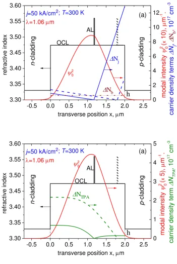
Figure 3 shows the distribution of the different carrier density contributions in the structure of
Figure 1a for both positions of the active layer shown in the figure (with the waveguide structure
and the intensity distribution also repeated for reference) for the value of j=50 kA/cm2, which
towards the upper limit of what is realistically achievable. As the paper addresses the pulsed
operation regime, all the calculations were performed with room-temperature parameters, e.g. we
took De=200 cm2/s; Dh=10 cm2/s. As implied by the form of (13), in this part of the work, to
present a clear physical picture concentrating on the effects of TPA and carrier accumulation, we
used a longitudinally lumped model, not taking into account photon density distribution P(z) along
the cavity and thus longitudinal spatial hole burning (LSHB). We can however note in passing that
even in the case of LSHB present, there would always be a certain cross-section of the laser cavity
(a certain value of z) for which the local value of power, and hence the carrier density distribution,
would correspond to that presented in Figure 3.
It is clear from Figure 3 that, in addition to current, both the form of the carrier density distribution
- 16 -
layer with respect to the p-cladding. If the active layer is positioned near the centre of the OCL, the
slow ambipolar diffusion in the broad p-OCL leads to very significant values of Nj, with
j x h N
reaching values of the order of 1018 cm-3, as already discussed in earlier papers [16, 17, 26].
Conversely, the TPA-created carrier density is in this case efficiently depleted, due to the fact that
the carrier drain due to the capture into the AL is spatially very close to the point of the maximum
TPA generation (the modal peak).
As the AL is shifted towards the p-cladding (la is increased), the p-OCL becomes narrower and the
n-OCL (in which the slope of N xj( ) as described by Eq. (9) is much lower than in the p-OCL
since De> > Dh), correspondingly wider; therefore overall, the effect of Nj in the waveguide is
significantly reduced. Meanwhile, the TPA-created carriers become less efficiently depleted with
an increased la as their generation and drain become increasingly separated in space. This leads to a
substantial increase inNTPA which at the very high current shown in the figure actually exceeds
j N
throughout the n-OCL (in the p-OCL, NTPA conversely becomes very low, but as the p-OCL
is now much narrower than the n-OCL, this has less effect on the absorption). It has to be noted
however that even in the case of the AL near the p-cladding, the effect of the TPA-created carriers
is substantially smaller than that used in the papers [22] [23] where the capture of the TPA-created
carriers into the AL (and thus the nature of their spatial distribution) was ignored, as was the
current-generated carrier population, both uniform and nonuniform, and carrier density was
(implicitly) determined by the carrier recombination time in the OCL.
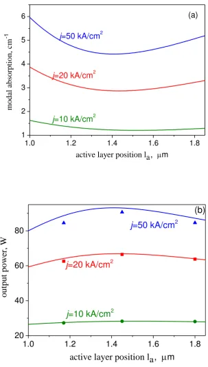
As can be expected, the tendencies discussed above are reflected in the dependence of the various
contributions to the internal loss on the active layer position la, which is shown in Figure 4 for the
current density value of j=50 kA/cm2. As discussed above, (jFC) decreases as the AL is shifted
built-- 17 built--
in losses and the direct TPA contribution) are virtually independent of la (the weak parametric
dependence of (mod) TPA
on la is due to the dependence of the power on la in the self-consistent
calculation). There is thus an optimal AL position that minimises the losses for a given current
density value, though the optimum is neither sharp nor very pronounced – the combination of (jFC)
and (FC) TPA
with their opposite dependence on la leads to the dependence of the total loss on the
active layer position being much weaker than that of either (jFC)or (FC) TPA
on their own.
Figure 5 shows the la dependence of total losses (Figure 5a) and the corresponding power values
(Figure 5b) for three current density values. The minimum of loss (or maximum of power)
discussed above is seen at all current values studied; its position shifts somewhat away from the
p-cladding and towards the centre of the OCL as the current is increased, though only slightly,
because of the sublinear dependence P(j).
As in the case of Figure 3, to calculate P(j) in all subsequent figures we mainly used a
self-consistent procedure including all the nonlinear loss mechanisms discussed here, but using the
lumped approximation (13) ignoring the longitudinal power variation P(z); those are the results
shown as lines. We have verified that for the values of the laser cavity geometry parameters L and
w and antireflection and high-reflection coated facet reflectance coefficients RAR, RHR (often used in
practice, see e.g. [5, 24]) used in the calculations, the lumped model provides good accuracy, not
just qualitatively, but quantitatively as well. As an illustration, Figure 5 includes, in addition to the
lines, also results calculated for the three representative active layer positions (la= 1.17 µm near the
OCL centre and la= 1.8 µm near the p-cladding as in Figure 1a, and in addition la= 1.45 µm near the
optimum) using a distributed model similar to those of [22, 23, 29] ) with power P, and hence TPA(FC)
and (mod) TPA
, calculated locally, as functions of z. These are represented as filled dots in Figure 5b.
- 18 -
slightly modifies the calculated power, the modification is small (about 4% at the highest current)
and does not affect the dependence of power on la , including the position of the optimum. More
detailed analysis, including treating laser structures with longer cavities and/or lower RAR, where
LSHB can be somewhat more important [30], is reserved for further work.
The results imply therefore that there is a design of the laser waveguide (the active layer position la)
that would be near enough to the optimal position for high-power operation in a broad range of
currents.
This is confirmed by Figure 6 which shows calculated losses as function of current with the active
layer position as a parameter; it is seen that the loss value for la=1.45 µm, which is close to optimal
for all values of j, stays below the loss calculated for the two “extreme” positions (near the centre of
the waveguide and near the p-cladding) within the whole range of current densities.
Finally, Figure 7 shows the light-current curves calculated for various active layer positions and
different effects taken into account. The dashed line in all graphs is a linear curve taking into
account only built-in losses. As can be expected from Figures 4-6, for the near-central position of
the active layer (la=1.17 µm, Figure 7a) as well as for la=1.45 µm, (Figure 7b) the main deviation
of the light-current curve from the linear approximation is due to carrier build-up because of current
((jFC)), whereas for the case of the AL near the p-cladding (la=1.8 µm, Figure 7c), the carrier
accumulation due to TPA and the corresponding loss mechanism TPA(FC) are at least as important as
(FC) j
. Also as implied by Figure 6, the power output is the highest, of the three cases presented, for
the near-optimum active layer location (la=1.45 µm).
It has to be noted that Figures 6-7 were calculated assuming that the laser in all cases operates in a
single, fundamental transverse mode at all currents. For the case of la=1.17 µm, this can indeed be
- 19 -
other two positions, reliable single-mode operation cannot be guaranteed and operation in the
second order mode, at least for lower currents, as discussed in [31], cannot be ruled out. In this
case, double asymmetry of the laser structure, with both the active layer position and the refractive
index profile (as in Figure 1b) being asymmetric, is necessary to ensure reliable fundamental mode
operation. Detailed optimisation is reserved for future work, but it can be expected that the
optimum position of the active layer will be not too different from the one obtained for the
symmetric waveguide.
4. Conclusions.
We have developed an efficient semi-analytical approach to analyse the direct ( (mod) TPA
) and indirect
( (FC) TPA
, due to free carrier absorption by TPA-created carriers) TPA contributions to optical losses
in high power laser diodes as functions of laser structure and operating conditions, taking into
account the structure geometry and the effects of carrier transport which we identified as the main
mechanism of drain for TPA-created carriers.
Both of the TPA effects were found to be less important than the optical loss (jFC) due to
current-induced inhomogeneous carrier accumulation for broad waveguides with the active layer positioned
approximately symmetrically in an undoped OCL. We found however that the TPA became more
important for those structures where the AL is located nearer the p-cladding. In this latter case, the
indirect TPA effect was shown to become more important than both the direct one and the effect of
current induced carrier accumulation in determining the output power: TPA(FC)TPA(mod); TPA(FC)(jFC),
which agrees qualitatively with the experimental findings for SCOW amplifiers [20]. Therefore, in
general, both (jFC) and the TPA effects need to be taken into account when optimising the laser
structure for high power pulsed operation. Indeed, the combination of the different dependences of
(FC) TPA
- 20 -
active layer position la, located between the centre of the OCL and the p-cladding and relatively
weakly dependent on current.
In its present form, the analysis is restricted to laser designs where most of the optical mode
intensity resides in the OCL; however, we believe the findings are generic enough to be important
- 21 -
Appendix 1. Expressions for the waveguide mode and the carrier density distribution.
In the simulations, the modal profile ( )x (as shown in figures), and the modal refractive index n0
were obtained for the sake of generality from a multilayer mode solver including the waveguiding
properties of the active layer, but we verified that the results were very close to those obtained in a
simple three-layer slab waveguide model, since da< < h. In that model, the expressions for ( )x
can be taken from Ref. [25] and is given by Eq. (3)a-c in the main text.
The value of n0 is found from the usual transcendental equation
arctan n arctan p
h
(A1.1)
where
, n, pare functions of n0 as described in the main text.This form of ( ) x results in the expression for the TPA parameter 4( )x dx 1/hTPA
in the form
1 2
4 4
1 3 1 1 1 1
sin 2( ) sin sin 4( ) sin 4
2 8 8
cos cos ( )
TPA eff
n p
h h h h
h h
(A1.2)For the TPA-induced carrier distribution, the double integration of the generation term with the zero
boundary conditions as in the main text gives for the n-OCL (0<x<la):
2
2 1 2 2
( ) 3 1 1
( , ) cos 4( ) cos 2( )
8 2 16
TPA n n
a B z
N x z C C x x x x
D
- 22 - with
1
1
8sin 2 sin 4 ; 4
n
C
(A1.4a)
2
2 1 2 2
3 1 1
cos 4( ) cos 2( )
2 16
n a n a a a
C l C l l l
(A1.4b)
For the p-OCL (la <x<h):
2
2 1 2 2
( ) 3 1 1
( , ) cos 4( ) cos 2( )
8 2 16
TPA p p
a B z
N x z C C x x x x
D
(A1.5)
with
1
2 1
3 sin 2( ) sin 4( )
4 p
C h h h
(A1.6a)
2
2 1 2 2
3 1 1
cos 4( ) cos 2( )
2 16
p a p a a a
C l C l l l
, ( A1.6b)
where in all expressions,
2 2
4 ( ) ( )
( )
eff
x P z
B z h w
( A1.7)
- 23 -
Figure captions
Figure 1. Schematic of the structures evaluated and the corresponding intensity distributions in the
(fundamental) waveguide mode: (a) the symmetric waveguide (with two active layer positions
shown approximately indicating the range studied); (b) the asymmetric waveguide
Figure 2. The waveguide (OCL) thickness dependence of the TPA parameter for symmetric (a) and
asymmetric (b) waveguides shown in Figure 1. Solid: exact calculation, dashed - Gaussian
approximation of the transverse mode profile, dash-dotted - top-hat approximation.
Figure 3. Calculated spatial distributions of t contributions to the carrier density in the OCL due to
current (a) and TPA(b). Solid: la=1.17 µm; dashed: la=1.8 µm. The waveguide profile and modal
distribution (for la=1.17 µm) shown for reference.
Figure 4. Dependence of the total modal absorption and its constituent parts on the active layer
position la for the waveguide of Figure 1a and the current density of j= 50 A/cm2 (current i=150 A)
Figure 5. Dependence of the total modal absorption (a) and the corresponding laser output power
(b) on the active layer position la for the waveguide of Figure 1a and three values of carrier density.
Solid lines are calculated in the lumped laser model, dots in a distributed model taking into account
Longitudinal Spatial Hole Burning.
Figure 6. Carrier density dependences of the total modal absorption in the waveguide of Figure 1a
and for the three positions of the active layer shown as dots in Figure 5b. Cavity length L= 3 mm,
stripe width w = 100 µm
Figure 7. Output power vs current curves calculated for a laser of Figure 1a, with the cavity length
L= 3 mm and stripe width w = 100 µm, for the three positions of the active layer shown in Figures
- 24 -
contributions: (1)
in(built in) only; (2)
in(built in)
(FC)j ; (3)
in(built in)
(FC)j
TPA(mod); (4) allnonlinear effects:
in
in(built in)
(FC)j
TPA(FC)
TPA(mod) - 25 -
Table 1. The main source parameters and their values.
symbol parameter Value
photon energy 1.17 eV ( =1.06 µm)
nOCL OCL refractive index 3.474
nn n-cladding refractive index 3.464 (asymmetric)
3.300 (symmetric)
np p-cladding refractive index 3.300
( ) 2
OCL
TPA coefficient in the OCL 210-8 cm/W
L cavity length 3 mm
w stripe width 100 µm
RAR AR coated facet reflectance 0.05
RHR HR coated facet reflectance ≈1
h waveguide thickness 2 µm (Section 3)
e free-electron absorption cross section 310-18 cm2
h Free-hole absorption /IVBA
cross-section
110-17 cm2
De electron diffusion coefficient 200 cm2/s
Dh hole diffusion coefficient 10 cm2/s
- 26 -
Figures.
-0.5 0.0 0.5 1.0 1.5 2.0 2.5
3.25 3.30 3.35 3.40 3.45 3.50 3.55 3.60 0.0 0.2 0.4 0.6 0.8 1.0 (a) mod al in ten si ty
2 , 0
m -1 re fra ct iv e i nd ex
distance x, m
n -c la dd in g p -c la dd in g
Optical confinement layer
active layer positions
1 2
-1.5 -1.0 -0.5 0.0 0.5 1.0 1.5 2.0 2.5 3.25 3.30 3.35 3.40 3.45 3.50 3.55 3.60 0.0 0.2 0.4 0.6 mod al in ten si ty
2 , 0
m -1 re fra ct iv e i nd ex
distance x, m
[image:27.595.148.448.159.622.2]- 27 -
0
1
2
3
4
5
0.0 0.5 1.0 1.5 2.0 2.5 3.0
Symmetric structure
exact Gaussian top-hat TP A par ame ter 1/ h T PA , m -1OCL thickness
h
,
m
0.0 0.5 1.0 1.5 2.0 2.5 3.0
(a)
0 1 2 3 4 5
0.0 0.2 0.4 0.6 0.8 1.0 Asymmetric structure exact top-hat TP A par ame ter 1/ h T PA , m -1
OCL thickness h, m
- 28 -
-0.5 0.0 0.5 1.0 1.5 2.0 2.5
3.30 3.35 3.40 3.45 3.50 3.55 3.60 0 2 4 6 8 10 12
NbAL 2 0 ca rr ie r d en si ty te rms
N j ,
N b , 10 17 cm -3h
mod al in ten si ty
2 ( 0
x 10 ), m -1 . refractive index
transverse position x, m
n -c la dd in g p -c la dd in g OCL
j=50 kA/cm2; T=300 K
N
j(a)
=1.06 m
-0.5 0.0 0.5 1.0 1.5 2.0 2.5
3.30 3.35 3.40 3.45 3.50 3.55 3.60 0 1 2 3 4 5 (a) AL 2 0
NTPAca rr ie r d en si ty te rm
N T PA , 10 17 cm -3h
mod al in ten si ty
2 ( 0
x 5) , m -1 . refractive index
transverse position x, m
n -c la dd in g p -c la dd in g OCL
j=50 kA/cm2; T=300 K
[image:29.595.130.482.91.613.2]=1.06 m
- 29 -
1.0 1.2 1.4 1.6 1.8
0 1 2 3 4 5 6
built-inin
(mod)TPA
(FC)TPA
modal absorption,
cm
-1
active layer position la, m j=50 kA/cm2
total
(FC) [image:30.595.162.420.97.308.2]j
- 30 -
1.0 1.2 1.4 1.6 1.8
1 2 3 4 5 6
j=10 kA/cm2
j=20 kA/cm2
j=50 kA/cm2
m
o
d
al
ab
so
rp
ti
o
n
,
cm
-1
active layer position la, m
(a)
1.0 1.2 1.4 1.6 1.8
20 40 60 80
j=10 kA/cm2
j=20 kA/cm2
j=50 kA/cm2
output power,
W
active layer position la
,
m [image:31.595.146.450.110.644.2](b)
- 31 -
0 10 20 30 40 50
0 1 2 3 4 5
modal absorption,
cm
-1
current density, kA/cm2
[image:32.595.144.435.171.394.2]l
a=1.17 m 1.45 m 1.8 m- 32 -
0 20 40 60 80 100 120 140
20 40 60 80 100 120 140 20 40 60 80 100 120 140
l
a=1.17 m3 2 1 po we r, W
current i, A
4 (b)
0 20 40 60 80 100 120 140
20 40 60 80 100 120 140 20 40 60 80 100 120 140
l
a=1.8 m3 2 1 po we r P , W
current i, A
4 (c)
0 20 40 60 80 100 120 140
20 40 60 80 100 120 140
l
a=1.17 m3 2 1 po we r P , W
current i, A
4
(a)
0 10 20 30 40 50
current density, kA/cm2
- 33 -
References.
[1] I. S. Tarasov, "High-power semiconductor separate-confinement double heterostructure lasers,"
Quantum Electronics, vol. 40, pp. 661-681, 2010 2010.
[2] P. Crump, G. Erbert, H. Wenzel, C. Frevert, C. M. Schultz, K. H. Hasler, et al., "Efficient High-Power
Laser Diodes," IEEE Journal of Selected Topics in Quantum Electronics, vol. 19, Jul-Aug 2013.
[3] M. R. Gokhale, J. C. Dries, P. V. Studenkov, S. R. Forrest, and D. Z. Garbuzov, "High-power
high-efficiency 0.98-mu m wavelength InGaAs-(In)GaAs(P)-InGaP broadened waveguide lasers grown by
gas-source molecular beam epitaxy," Ieee Journal of Quantum Electronics, vol. 33, pp. 2266-2276,
Dec 1997.
[4] A. Al-Muhanna, L. J. Mawst, D. Botez, D. Z. Garbuzov, R. U. Martinelli, and J. C. Connolly,
"High-power (> 10 W) continuous-wave operation from 100-mu m-aperture 0.97-mu m-emitting Al-free
diode lasers," Applied Physics Letters, vol. 73, pp. 1182-1184, Aug 1998.
[5] N. A. Pikhtin, S. O. Slipchenko, Z. N. Sokolova, A. L. Stankevich, D. A. Vinokurov, I. S. Tarasov, et al.,
"16W continuous-wave output power from 100 mu m-aperture laser with quantum well
asymmetric heterostructure," Electronics Letters, vol. 40, pp. 1413-1414, Oct 2004.
[6] D. A. Vinokurov, S. A. Zorina, V. A. Kapitonov, A. V. Murashova, D. N. Nikolaev, A. L. Stankevich, et
al., "High-power laser diodes based on asymmetric separate-confinement heterostructures,"
Semiconductors, vol. 39, pp. 370-373, Mar 2005.
[7] A. Knauer, G. Erbert, R. Staske, B. Sumpf, H. Wenzel, and M. Weyers, "High-power 808 nm lasers
with a super-large optical cavity," Semiconductor Science and Technology, vol. 20, pp. 621-624, Jun
2005.
[8] L. Fan, C. S. Cao, G. Thaler, B. Caliva, I. Ai, S. Das, et al., "Record High-Temperature Long-Pulse
Operation of 8xx-nm Diode Laser Bar with Aluminum-Free Active Region," Ieee Journal of Selected
Topics in Quantum Electronics, vol. 17, pp. 1727-1734, Nov-Dec 2011.
[9] P. W. Juodawlkis, J. J. Plant, W. Loh, L. J. Missaggia, F. J. O'Donnell, D. C. Oakley, et al., "High-Power,
- 34 -
Applications," Ieee Journal of Selected Topics in Quantum Electronics, vol. 17, pp. 1698-1714,
Nov-Dec 2011.
[10] B. Lanz, B. S. Ryvkin, E. A. Avrutin, and J. T. Kostamovaara, "Performance improvement by a
saturable absorber in gain-switched asymmetric-waveguide laser diodes," Optics Express, vol. 21,
pp. 29780-29791, Dec 2013.
[11] Y. Yamagata, Y. Yamada, M. Muto, S. Sato, R. Nogawa, A. Sakamoto, et al., "915nm high power
broad area laser diodes with ultra-small optical confinement based on Asymmetric Decoupled
Confinement Heterostructure (ADCH)," in High-Power Diode Laser Technology and Applications Xiii.
vol. 9348, M. S. Zediker, Ed., ed, 2015.
[12] K. H. Hasler, H. Wenzel, P. Crump, S. Knigge, A. Maasdorf, R. Platz, et al., "Comparative theoretical
and experimental studies of two designs of high-power diode lasers," Semiconductor Science and
Technology, vol. 29, Apr 2014.
[13] M. Buda, T. G. vandeRoer, L. M. F. Kaufmann, G. Iordache, D. Cengher, D. Diaconescu, et al.,
"Analysis of 6-nm AlGaAs SQW low-confinement laser structures for very high-power operation,"
Ieee Journal of Selected Topics in Quantum Electronics, vol. 3, pp. 173-179, Apr 1997.
[14] B. S. Ryvkin, E. A. Avrutin, and J. T. Kostamovaara, "Narrow versus broad asymmetric waveguides
for single-mode high-power laser diodes," Journal of Applied Physics, vol. 114, Jul 2013.
[15] B. Ryvkin, E. A. Avrutin, and J. T. Kostamovaara, "Asymmetric-Waveguide Laser Diode for
High-Power Optical Pulse Generation by Gain Switching," Journal of Lightwave Technology, vol. 27, pp.
2125-2131, Jun 2009.
[16] B. S. Ryvkin and E. A. Avrutin, "Asymmetric, nonbroadened large optical cavity waveguide
structures for high-power long-wavelength semiconductor lasers," Journal of Applied Physics, vol.
97, Jun 2005.
[17] B. Ryvkin and E. Avrutin, "Non-uniform carrier accumulation in optical confinement layer as
ultimate power limitation in ultra-high-power broad-waveguide pulsed InGaAs/GaAs/AlGaAs laser
- 35 -
[18] D. Z. Garbuzov, A. V. Ovchinnikov, N. A. Pikhtin, Z. N. Sokolova, I. S. Tarasov, and V. B. Khalfin,
"Experimental and theoretical investigations of singularities of the threshold and power
characteristics of ingaasp/inp separate-confinement double-heterostructure lasers (lambda = 1.3
mu-m)," Soviet Physics Semiconductors-USSR, vol. 25, pp. 560-564, May 1991.
[19] B. Ryvkin and E. Avrutin, "Heating-induced carrier accumulation in the optical confinement layer
and the output power in broadened symmetric and narrow asymmetric waveguide laser diodes,"
Journal of Applied Physics, vol. 101, Jun 2007.
[20] P. W. Juodawlkis, J. J. Plant, J. P. Donnelly, A. Motamedi, and E. P. Ippen, "Continuous-wave
two-photon absorption in a Watt-class semiconductor optical amplifier," Optics Express, vol. 16, pp.
12387-12396, Aug 2008.
[21] A. R. Motamedi, J. J. Plant, J. P. Donnelly, P. W. Juodawlkis, and E. P. Ippen, "Ultrafast nonlinearities
and gain dynamics in high-power semiconductor amplifiers," Applied Physics Letters, vol. 93, Dec
2008.
[22] M. Dogan, C. P. Michael, Y. Zheng, L. Zhu, and J. H. Jacob, "Two photon absorption in high power
broad area laser diodes," Proceedings of SPIE, vol. 89650P, 2014.
[23] A. Demir, M. Peters, R. Duesterberg, V. Rossin, and E. Zucker, "Semiconductor Laser Power
Enhancement by Control of Gain and Power Profiles," Ieee Photonics Technology Letters, vol. 27,
pp. 2178-2181, Oct 15 2015.
[24] D. A. Veselov, N. A. Pikhtin, A. V. Lyutetskiy, D. N. Nikolaev, S. O. Slipchenko, Z. N. Sokolova, et al.,
"Effect of laser cavity parameters on saturation of light-current characteristics of high-power pulsed
lasers," Quantum Electronics, vol. 45, pp. 597-600, 2015.
[25] H. Kogelnik, "Theory of dielectric waveguides," in Integrated Optics, T. Tamir, Ed., ed Berlin
Heidelberg New York: Springer-Verlag, 1975, pp. 15-79.
[26] B. S. Ryvkin and E. A. Avrutin, "Effect of carrier loss through waveguide layer recombination on the
internal quantum efficiency in large-optical-cavity laser diodes," Journal of Applied Physics, vol. 97,
- 36 -
[27] N. K. Dutta, "Calculated temperaure dependence of threshold current of GaAs-AlXGa1-XAs double
heterostructure lasers," Journal of Applied Physics, vol. 52, pp. 70-73, 1981.
[28] C. Y. Tsai, C. Y. Tsai, Y. H. Lo, R. M. Spencer, and L. F. Eastman, "Nonlinear gain coefficients in
semiconductor quantum-well lasers - effects of carrier diffusion, capture, and escape," IEEE Journal
of Selected Topics in Quantum Electronics, vol. 1, pp. 316-330, Jun 1995.
[29] B. S. Ryvkin and E. A. Avrutin, "Spatial hole burning in high-power edge-emitting lasers: A simple
analytical model and the effect on laser performance," Journal of Applied Physics, vol. 109, Feb
2011.
[30] H. Wenzel, "Basic Aspects of High-Power Semiconductor Laser Simulation," IEEE Journal of Selected
Topics in Quantum Electronics, vol. 19, Sep-Oct 2013.
[31] E. A. Avrutin, B. S. Ryvkin, A. S. Payusov, A. A. Serin, and N. Y. Gordeev, "Fundamental transverse
mode selection and self-stabilization in large optical cavity diode lasers under high injection current