Consideration for Delay-based Power Gating Test
Vasileios Tenentes,
Member
,
IEEE
, Saqib Khursheed,
Member
,
IEEE
, Daniele Rossi,
Member
,
IEEE
,
Sheng Yang,
Member
,
IEEE
, and Bashir M. Al-Hashimi,
Fellow
,
IEEE
Abstract—This paper shows that existing delay-based testing techniques for power gating exhibit both fault coverage and yield loss due to deviations at the charging delay introduced by the distributed nature of the power-distribution-networks (PDNs). To restore this test quality loss, which could reach up to 67.7% of false passes and 25% of false fails due to stuck-open faults, we propose a design-for-testability (DFT) logic that accounts for a distributed PDN. The proposed logic is optimized by an algorithm that also handles uncertainty due to process variations and offers trade-off flexibility between test-application-time and area cost. A calibration process is proposed to bridge model-to-hardware discrepancies and increase test quality when considering systematic variations. Through SPICE simulations, we show complete recovery of the test quality lost due to PDNs. The proposed method is robust sustaining 80.3% to 98.6% of the achieved test quality under high random and systematic process variations. To the best of our knowledge, this paper presents the first analysis of the PDN impact on test quality and offers a unified test solution for both ring and grid power gating styles.
Index Terms—power gating, dft, power-distribution-network, test quality, grid style, ring style, systematic variations
I. INTRODUCTION
Power gating is a low power design technique for integrated circuits (ICs) that assures the viability of high performance and energy efficient electronic devices at sub-100-nm CMOS technologies [1]. It utilizes transistors as power-switches of logic blocks supply voltage to reduce leakage power and power consumption during periods of inactivity. Power switches are susceptible to defects and their high quality testing is crucial for the efficient low power performance of power-gated ICs, for silicon debugging, for yield analysis and for improving subsequent manufacturing cycle [2]–[5]. Design-for-testability (DFT) is a design technique for assuring the quality of testing of ICs for physical defects during their lifetime from the manufacturing to the field. It consists of
fault models that mimic the behavior of physical defects and
DFT logic structures that provide the engineering means to apply the tests and collect back their responses.
Power switches are implemented as header or footer switches in either fine-grain or coarse-grain design styles. A fine-grain style incorporates a power switch within each logic cell simplifying power gating synthesis through existing
V. Tenentes, B. M. Al-Hashimi, D. Rossi and S. Yang are with the Department of Electronics and Computer Science, University of Southamp-ton, Southampton SO17 1BJ, U.K. (e-mails: {V.Tenentes, bmah, D.Rossi, sheng.yang}@ecs.soton.ac.uk)
S. Khursheed is with the Department of Electrical Engineering and Elec-tronics, University of Liverpool, U.K. (e-mail: [email protected])
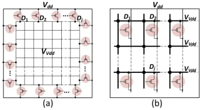
Fig. 1. (a) Ring style and (b) grid style power gating schemes.
EDA tools [6]. However, thecoarse-graindesign style is more popular and the focus of this work, since it requires less silicon and offers higher robustness against process variations.
Coarse grain power gating is implemented in two different design styles by deploying either a ring or a grid network of power switches. Inring style[6], power switches are placed at a ring externally to the power-gated block (Figure 1(a)). Ingrid style [6], [7], power switches are distributed throughout the power-gated region (Figure 1(b)) forming a grid between the power-distribution-networks (PDNs): the supply voltage Vdd
PDN (SPDN) and the virtual voltage VV dd PDN (VPDN). When comparing these two styles [6], the ring is the only option for power gating IP blocks, while the grid style is the only one scalable to large designs and the only option that supports state retention. This paper considers both styles.
Power switches may operate in two low power modes which provide a trade-off between leakage power saving and wake-up time: complete power-off mode (higher leakage power saving) and intermediate power-off mode (lower wake-up time). Recent research has reported a number of DFT solutions to test power switches when considering the stuck-open [8]– [12] and the stuck-short [13], [14] fault models. Stuck-short faults produce a conducting path between Vdd and ground and testing against them is crucial to sustain the low power consumption benefits of power gating. Stuck-shorts impact the steady state current at power-off mode and could be detected by anIDDQbased method. Digital-based DFT for monitoring the voltage level of power switches at intermediate mode steady-state have been recently proposed [13], [14]. Stuck-open faults model a defect where the drain or source of a transistor is disconnected. Their testing is crucial for assuring that the power-gated domain will not suffer from small delays due to power-grid IR-drop. In this paper, we target the
[image:1.612.336.532.189.297.2]Fig. 2. (a) DFT with lumped PDNs [15] and (b) stuck-opens test process.
opens through measuring the power-off to power-on delay. Although previous works have considerably advanced the DFT techniques for power switches, they rely on lumped RC models of the PDNs without considering their distributed nature. It was shown in [16] that, at the grid style power gating, this simplification interacts with the test result and in [17] that could even influence the diagnosis result. In Section II, we consider a distributed model for the RC components of the supply voltage PDN (SPDN), the ground voltage PDN (GPDN) and the virtual voltage PDN (VPDN). We examine both the ring and the grid power gating styles, shown in Figure 1(a) and in Figure 1(b), respectively. Based on this setup, in Section III, we show that the lumped model shortcut used by the state-of-the-art [8], [9], [15] may lead to both fault coverage loss and yield loss that may reach up to 67.7% and 25%, respectively, and we analyze the reasons of this
test quality loss. To tackle this problem, Section IV presents a DFT architecture that considers a distributed PDNs model and restores the test quality (fault coverage and yield) at low cost. Its overhead is optimized by an algorithm that offers trade-off flexibility between test-application-time (TAT) and area cost. In Section V we adapt the proposed DFT design method to handle uncertainty and we propose a calibration method from post-silicon measurements that also handles systematic variations. Section VI evaluates the performance and presents the trade-offs of the proposed method and Section VII concludes the paper.
[image:2.612.52.293.57.287.2]II. STATE-OF-THE-ART& DISTRIBUTEDPDNS Figure 2(a) presents the state-of-the-art DFT architecture for delay-based testing against stuck-open faults on header power switches [8], [9], [15]. The power switches are clustered in m segments-under-test (SUTs) of segment-size L power switches [9]. The test process, shown in Figure 2(b), starts with the initialization phase, during which the control logic fully
Fig. 3. Setup for power gating segmentation: (a) ring style; (b) grid style.
TABLE I
RCELEMENTS FORLUMPED ANDDISTRIBUTEDPDN MODELS
style & model ethernet s38417
ring
style
PDN virtual supply ground virtual supply ground
lump.
R (Ω) 4.9E-08 1.6E-07 3.9E-08 1.4E-07 8.5E-07 9.8E-08 C (F) 9.4E-12 2.2E-12 1.8E-11 2.4E-12 1.9E-13 5.5E-12
distrib
uted
R
count 90859 18741 109339 27540 3136 39255 min 0.001 0.001 0.001 0.001 0.001 0.001 (Ω) max 19.1 150.5 1203.8 6.8 13.8 338.0
C
count 52678 9332 91003 17158 1664 55333 min 5.9E-23 2.3E-20 4.1E-24 2.1E-23 2.0E-19 4.3E-23 (F) max 5.8E-15 3.2E-14 1.8E-14 2.8E-14 2.7E-14 4.8E-14
grid
style
lump.
R (Ω) 6.4E-08 3.2E-08 4.9E-08 2.8E-07 1.4E-07 1.9E-07 C (F) 9.7E-12 1.0E-11 1.7E-11 1.7E-12 1.5E-12 3.7E-12
distrib
uted
R
count 70528 77542 92444 15790 17891 26821 min 0.001 0.001 0.001 0.001 0.001 0.001 (Ω) max 25.9 145.4 760.7 13.9 5.6 294.2
C
count 35294 55307 59457 14239 8720 33578 min 3.7E-22 8.5E-23 3E-22 8.6E-23 1.0E-20 6E-23 (F) max 6.1E-15 1.8E-14 1.2E-14 2.8E-14 2.1E-14 1.6E-14
discharges the VV dd node by using the discharge transistors [8]. During the application phase, a single SUTSiis awakened by the control logic by deasserting the sleepi signal. Upon the capture moment, the NAND gate logic output is captured at the “test result” flip-flop by asserting the test clock [15], the frequency of which depends on the segment size L. The captured value indicates whether the observation point VV dd was sufficiently charged at the capture moment. Test clock frequency is selected based on theobservable charging delay M of theVV ddpoint, hereafter referred to asobservable
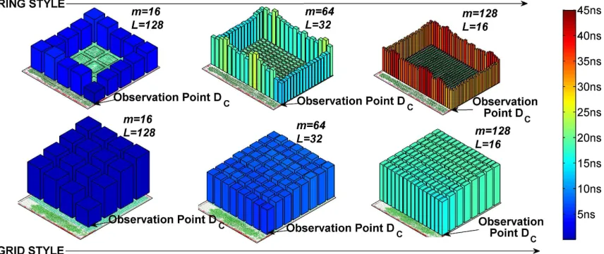
[image:2.612.313.566.64.352.2]Fig. 4. The observable charging delayMiC at observation pointDC(right corner of the power domain marked with an arrow) for every SUTSion ring
and grid power gating styles for three segmentation setups:L×m= 128×16,32×64and16×128.
moment, when the transient voltage at the NAND gate output reaches logic-0 value under the fault-free scenario. The voltage level of ≤ 0.2VV dd is used at the illustrations of the paper. However, this point is within 20%-80% ofVdd [18]. Note that based on the PDNs lumped models shown in Figure 2(a), the observable charging delay is computed the same for all SUTs.
We analyzed a large number of benchmarks from the IWLS’05 benchmark suite [19] and selected three represen-tatives: the ethernet, the s38417 and the s38584 benchmark circuits. These circuit comprises 157.5K, 30.5K and 26.9K gate equivalents, respectively, with a gate equivalent corre-sponding to a two input NAND gate. To generate the RC distributed model of SPDN, GPDN and VPDN, we synthesize the circuits using a 90nm library and operational voltage of
Vdd = 1.2V for both ring and grid power gating styles using header power switches. The constraint set during the physical synthesis of the PDNs is to achieve ≤ 10% IR drop for the ring and 5% for the grid style using 2048 power switches for the ethernet and 512 power switches for the s38417 and s38584 circuits. This leads to similar power rails size for the two styles. Then, using Synopsys STAR-RCXT, we extract a SPICE model for each style, shown in Figure 3(a) for ring and in Figure 3(b) for grid style, that includes both the nets and the power distribution networks of the design. GPDN is omitted from the Figure for clarity. Table I shows the RC elements information for the distributed and lumped models of the ethernet and the s38417 circuits. For the distributed model the number of R and C elements (count) and their range of value ([min, max]) is shown. The R and C values of the lumped model were computed assuming that the elements of the PDNs are connected in parallel (C=C1+C2+. . .+CN and1/R= 1/R1+ 1/R2+. . .+ 1/RN). Note that the high number of distributed RC elements for the distributed PDNs of the ethernet (more than 350 thousands) imply that their spatial effect should be considered for delay measurements. Thus, we cluster the power switches on both ring (Figure 3(a)) and grid (Figure 3(b)) power gating styles into SUTs according to a layout-driven approach: power switches that are closer to each
other are assigned to the same SUT. Finally, we integrate 200 uniformly scattered observation points Dj along the SUTs, shown as dots in Figure 3(a) and 3(b), for monitoring the observable wake-up times during simulations.
In this distributed environment, the wake up time may be measured through any of the observation points Dj on the VPDN (markedDj nodes in Figure 1(a) and in Figure 1(b)), an option not considered by the lumped model where the observation point is unique. In Section III we show that, when the distributed PDN model of Figure 3 is considered, the observable charging delay Mij depends on the observation point Dj and on the SUT Si. The deviations introduced by these factors negatively affect test quality with both fault coverage and yield loss.
III. ANALYSIS OFPDNSIMPACTONTESTQUALITY Through SPICE simulations of the distributed model pre-sented in Section II, we analyze the factors affecting the observable charging delay.
A. Dependence of charging delay on segment size L
Firstly, we consider the observable charging delay through a single observation point DC, located at the corner of the design and highlighted in Figure 3(a) and in Figure 3(b). Next, we simulate the test process for every SUT of each style and we gather the delays through a single observation pointDC. We obtain three sets of results for each style according to the following three segmentation setups of the 2048 power switches of the ethernet circuit: m×L= 16×128,64×32 and128×16. The results are presented in Figure 4 for both the ring (first row) and the grid style (second row), for the three considered segmentation setups. A bar in each graph presents the observable charging delayMiCthrough observation points
TABLE II
OBSERVABLE CHARGING DELAY DEVIATION FOR SYNTHESIZED DESIGNS
ethernet s38417 s38584
setup ring grid setup ring grid ring grid
[image:4.612.52.299.78.246.2]L×m M σ% M σ% L×m M σ% M σ% M σ% M σ% 128×16 5.9 21.2 2.5 23.5128×4 1.4 5.1 0.5 11.2 0.6 5.6 0.6 9.3 64×32 20.1 14.1 9.9 8.2 64×8 2.4 4.2 1 6.7 1.3 3.8 1.1 7.6 16×12835.1 11.9 19.7 4.6 32×164.5 2.7 1.9 4.8 2.34 3.2 2.2 4.1
Fig. 5. Observable charging delay from various observation points for activated SUT: (a) at the corner and (a) at the middle of the design.
of smaller size L delay the wake-up time. Consequently, the observable charging delayMij depends on the segment sizeL. Yet, from Figure 4 we derive that Mij depends on additional factors that are discussed next.
B. Dependence of charging delay on the activated SUTSi
In Figure 4, we observe that the charging delay varies even for a single segmentation setupL×m. For the ethernet circuit and for segmentation setup of L×M = 128×16, theMiC is in the ranges [3.57ns, 8.14ns] and [1.44ns, 3.59ns] for the ring and grid styles, respectively. From these graphs note that the charging delay MiC depends on the distance of the SUT to the observation point, as expected. Particularly, it depends on the RC components between the activated SUTSiand the observation point Dj. The activation of a SUT Si closer to the observation point DC, causes faster observable wake-up time. The same trend is observed for the rest of segmentation configurations. Consequently, the observable charging delay depends on the specific SUT Si.
Table II presents the observable delay variations of the benchmarks for both styles. For each circuit, the first column shows the examined segmentation setupL×m. The observable charging delay is presented with the average valueM between the minimum and maximum values of the range and the relative standard deviation σ. Note that for higher SUT sizes
L, the charging delay variation increases.
C. Dependence of charging delay on observation pointDj
Similarly, the observable charging delay of a SUT Si depends on the observation point through which it is observed. In Figure 5 we present the observable charging delay when two different SUTs are activated for the grid style segmentation setup of L×m = 64 ×32. The ‘x’ and ‘y’ axis are the location coordinates of the corresponding observation point in the die and the ‘z’ axis is the observable charging delay, when a SUT is activated. The first SUT (Figure 5(a)) is located at the corner of the design and exhibits observable charging delays
Fig. 6. Test quality degradation due to observationMijdeviation.
TABLE III
TESTQUALITYRESULTSUSING ASINGLECAPTUREMOMENT AND A
SINGLEOBSERVATIONPOINT
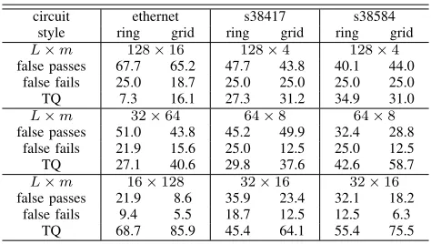
circuit ethernet s38417 s38584 style ring grid ring grid ring grid
L×m 128×16 128×4 128×4
false passes 67.7 65.2 47.7 43.8 40.1 44.0 false fails 25.0 18.7 25.0 25.0 25.0 25.0 TQ 7.3 16.1 27.3 31.2 34.9 31.0
L×m 32×64 64×8 64×8
false passes 51.0 43.8 45.2 49.9 32.4 28.8 false fails 21.9 15.6 25.0 12.5 25.0 12.5 TQ 27.1 40.6 29.8 37.6 42.6 58.7
L×m 16×128 32×16 32×16
false passes 21.9 8.6 35.9 23.4 32.1 18.2 false fails 9.4 5.5 18.7 12.5 12.5 6.3
TQ 68.7 85.9 45.4 64.1 55.4 75.5
in the range [8.3ns, 11.2ns] and the other one at the center (Figure 5(b)) in the range [9.5ns, 10.5ns]. Note, as expected, that when observation points are closer to the activated SUT the observable charging delay is lower.Thus, we conclude that both the choice of the observation pointDj and the activated
SUTSi impact considerably the observable wake-up time.
D. Test quality degradation
[image:4.612.319.556.264.398.2]Fig. 7. DFT design flow of the proposed method.
capture moment. The T Q is higher for small segment sizes, because the sensitivity of those setups (Table II) to observation point selection is lower. Note that as the size of a SUT increases, the sensitivity of the delay to observation point selection (Table II) increases and theT Qdecreases (Table III), rendering previous DFT methods inapplicable for high speed testing of power switches. These results clearly motivate the importance of a DFT architecture that considers the distributed PDNs nature. Therefore, Section IV presents a novel PDN-aware DFT architecture and a method to restore test quality.
IV. PROPOSEDPDN-AWAREDFT ARCHITECTURE
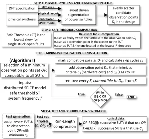
In this section we propose a PDN-aware DFT architecture that offers on-chip control of the parameters that affect the deviations of the observable wake-up time in order to restore test quality (TQ): the observation point Dj that observes that delay and the SUT Si. To avoid the need for multiple clock frequencies, the proposed DFT utilizes clock gating to generate variable capture moments. Practical heuristics are proposed to scale the DFT design method to large circuits and a compression scheme is proposed that reduces both the area cost of the DFT and the test application time (TAT).
A. DFT Design Flow
In Figure 7 we present thedesign flowof the proposed DFT architecture. It consists of four major steps described below.
1) Physical synthesis and segmentation setup: This step requires the power switches physical location, the distributed SPICE netlist and the segmentation setup L×m. Then, the power switches are clustered in SUTs of size L, driven by the layout, as described in Section II and shown in Figure 3. Observation points Dj of the VV dd are injected following layout driven evenly scattered intervals on the VPDN.
Fig. 8. (a) Safe threshold computation through single stuck-open fault injections. (b) Capture edges evaluation using the safe threshold.
2) Safe threshold computation: In Section II the basic scheme for testing power switches was described according to which the observation cell output is captured during capture moment by a flip-flop (Figure 6). Due to the factors that affect an observation, the capture moment will exhibit some deviation from the focal moment for at least some SUTs
Si. Recall from Section II that focal moment is the moment when the output of the NAND gate reaches logic-0. However, not all the deviations are harmful, if they do not affect test quality. Therefore, we introduce thesafe threshold(ST), a time threshold that represents the maximum acceptable deviation between the focal moment for observationMijand the capture moment. If ST is honored, neither false passes on single stuck open faults nor false fails are expected. The graph in Figure 8(a) shows how ST can be identified. The data of this graph correspond to the ethernet circuit and the segmentation setup of L×m = 128×16 of grid style (bottom-left graph of Figure 4). In Figure 8(a) the SUTS1 is observed through the
observation pointDC which is located very close to the SUT
S1 in the layout. The single darked shaded line on the left of
this graph shows the transient voltage at the observation point
DC under fault-free scenario, while the other lines belong to theLsingle-stuck open fault scenarios for every power switch in S1. The results show that the observation of the
[image:5.612.51.296.60.288.2]Fig. 9. Lowest skewLHon grid style of (a) corner SUT; (b) center SUT.
is captured, then it suffers from at least one fault.
It is worth noting that ST, which is the lowest delay skew LH of single stuck-open faults from the fault-free scenario, varies for every SUT Si and observation point selectionDj (STij). For large designs, fault simulating all the SUTs, even for single stuck-open faults, might lead to a formidable number of fault simulations. Therefore, to reduce the number of required fault simulations for the safe threshold ST computation, the following heuristics are proposed:
Heuristic h1: Fault simulate the farthest to the observation point power switch as faulty. From Figure 8(a) derives that the least skewed curve to the left belongs to the scenario where the faulty power switch is far from the observation point. Heuristic h2: Focus only at the observation point which is closer to a SUT Si. In Figure 9 the LH for two SUTs of the ethernet circuit at the grid style segmentation setup
L×m= 32×64 are presented for all possible single stuck open faulty scenarios. One SUT is located at the corner of the design (Figure 9(a)) and the other one is located at the center of the design (Figure 9(b)). The ‘x’ and ‘y’ axes denote the location of the observation point in the layout and the ‘z’ axis the lowest skew. In both cases the lowest skew is observed through the observation points closer to the activated SUT. Heuristic h3: Fault simulate the SUTs at the areas with the lowest IR-drop. Even with the two heuristics h1 and h2
every SUT should be fault simulated. Consider the graphs in Figure 9. The absolute value of the observed skew at the center (Figure 9(b)) SUT is lower compared to the SUT at the corner (Figure 9(a)) for the grid style architecture. The reason is that the SUT at the center is located at an area with lower IR-drop and it is more tolerant on faulty power switches compared to another SUT at an area with higher IR-drop. For the same reason, SUTs at areas with lower IR-drop (Figure 5(b)) exhibit less deviations on the observable charging delay compared to those at areas with higher IR-drop (Figure 5(a)). In our experiments we used this heuristic to obtain a global minimum ST for all SUTs and observation points. Note that this selection is pessimistic and a safe threshold per SUT and observation point STij could be used as an alternative, when fault simulations number is not the issue.
[image:6.612.310.565.62.181.2]Besides, we observe in Figure 9 that the lowest skew is exhibited very close to the SUT. A minimum distance constraint, for example excluding an observation point to be assigned to the SUT it belongs, between the observation point and the selected SUT leads to1.5×to2×larger safe threshold values. This feature benefits the robustness of the proposed method and reduces the observable charging delay deviations due to random noise on the RC parasitics of the PDNs.
Fig. 10. Example for observation points selection criteriaC1andC2.
3) Observation points selection: TheAlgorithm Iin Figure 7 selects a minimum observation points set OP so as for every SUT Si to be at least one OPj, the safe threshold of which is honored. This condition is refered to ascompatibility
and discussed below. The observable charging delay Mij is computed for every pair of SUTSiand candidate observation pointDj through simulations of the distributed model. Also, the TQ is affected by the capture moment. Therefore, the proposed architecture offers control over the selection of the capture moment by using the rising edges of the system clock. Hence, for every pair (Si,Dj) with observable charging delay
Mij, the system clock rising edges are evaluated for honoring the ST. If at least one rising edge honors ST, then the pair (Si,
Dj) is marked ascompatible. The clock edges that honor the ST are denoted as skip cyclescij. Note that minimum set of observation points OP must contain at least one compatible
OPj for every SUT Si to avoid TQ loss. This is guaranteed by iteratively applying the following two criteria that minimize the number of observation points|OP|(and consequently area cost) and TAT:
C1: Select the set of observation points Dj with the most compatible SUTs inS.
C2: Among thoseDj selected by criterionC1, select the one
that requires the minimumaverage number of skip cycles cij for all its compatible SUTs.
Any new observation point selection follows these criteria and its compatible SUTs are dropped from set S. The algorithm terminates when the setS is empty. If the designer has set the
more observation pointsparameter,M OP, to a value greater than the minimum number of observation points |OP|, the algorithm selects M OP number of observation points. This property offers a trade-off between area cost and TAT that will be shown in Section VI.
Example:Figure 10 presents a case of three SUTsS1, S2 and S3and three candidate observation pointsD1,D2andD3. The
clock edges honoring the safe thresholdSTij between a SUT and an observation point are shaded. Applying criterionC1on
this example leads to the selection of both observation points
D1 and D2, since these are compatible with all the SUTs,
while observation pointD3is compatible only withS2. Next,
criterion C2 is applied according to which the observation
Fig. 11. Proposed DFT architecture.
and for D2 is ci2 = (12 + 7 + 24)/3 = 14.3. Consequently, D1 is selected and added at set OP. Next, all compatible to D1 SUTs are dropped from set S. This action results in an
empty set S, since in this exampleD1 is compatible with all
the SUTs. Consequently, the algorithm ends. If the parameter
M OP was set toM OP = 2, an additional observation point would be selected. In this example,D3would also be selected,
since it qualifies for the first criterion on the empty set S
and it requires the less average number of clock cycles per compatible SUTs, since it is ci3 = 2/1 = 2. Now, SUT S2
can be tested spending fewer skip cycles through D3. Thus, M OP offers a trade-off between area cost and TAT. 4) Test and Control Data Generation: After the selection of the set OP, thetest generationprocess assigns every SUT
Si to acompatibleobservation point OPj. Since a SUT may be compatible to more than one observation points from the set OP, it selects the one with the minimum skip cycles cij in order to reduce TAT. In the example of Figure 10 SUTs
S1 andS3 are assigned to observation point OP1 =D1 and
SUT S2 to observation point OP2 = D3. Note that each
triplet of SUT Si, observation pointOPj and skip cycles cij is required to be stored on-chip in order to control the DFT logic. In Section VI-E we show that this area cost can become overwhelming, especially for setups with large SUTs number
m. To limit this overhead, we apply the following process that compresses these data using the Run-Length (RL) compression [20] and requires minimum decompression logic. The basic idea is that many SUTs Si require the activation of the same
OPj sinceOP set is selected to be minimum. We compress this correspondence (pairsSi,OPj) using the RL code and we store it on-chip in a register file OP-REG. Specifically, each entry OP-REG[j] stores the number of successive SUTs that
successive skip cycles. In this example the skip cyclescij= 5 suffice for testing all the SUTs. Therefore, each pair (Si,OPj) is assigned to the compatible skip cycle valuecijwith the most occurrences at all SUTs. In Section VI-E, we show that this action favors the RL compression efficiency. These control data are stored at the register file REG. Each entry C-REG[k] stores the skip cyclescijand the number of successive pairs that require the same skip cycles. In Section VI-E, we demonstrate the compression efficiency of this technique.
An alternative to reduce the compression scheme complex-ity is to omit the compression of the observation points assign-ment (OP-REG) and repeat every test from every observation point with the cost of TAT. However, part of the TAT spend could be restored after the post silicon calibration that is presented in Section V-B by reordering the observation points according to the number of their compatible SUTs.
Note that the above method requires the system clock fre-quency to evaluate and select the observation points. However, it is not affected by after speed-binning clock-frequency selec-tion, because manufacturing testing is conducted before speed binning and the testing is applied using a clock frequency provided by the PLL generator of the die [21].
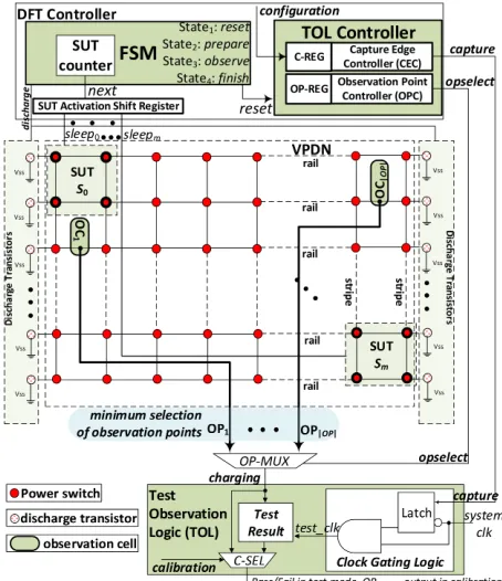
B. Architecture
The proposed DFT architecture is shown in Figure 11. It consists of four major blocks:
Test Observation Logic (TOL): This block generates the
capture edge and activates an observation point OPj out of a set of minimum observation pointsOP. Each SUT requires a different capture edge and OPj for 100% TQ. This unit latches system clock as long as thecapturesignal is zero and the multiplexer OP-MUX selects the appropriate observation pointOPj indicated by the opselect value. A flip-flop stores the test result, whencapture is asserted.
TOL Controller (TOLC): This block is responsible for
generating the control signalsopselectandcapturefor the TOL unit. First, the Observation Point Controller (OPC) generates on-chip theopselectsignal to control the activation of a single observation point for a particular SUT Si. The compressed data for the pairs Si and OPj are stored in a register file (OP-REG). Each register stores the opselect value and the number of successive SUTs that use it. Secondly, the Capture Edge Controller (CEC) generates on-chip the capture signal that controls the clock gating of the system clock. A counter counts down cij clock rising edges, denoted by skip cycles, before asserting capture. The skip cycles cij correspondence for each pair Si andOPj is also stored compressed in a C-REG register file. The C-C-REG contents are serially loaded with the skip cycles recomputed by the post-silicon calibration process, which is presented in Section V.
Observation Cells (OCs): The NAND observation cells,
alternatives like those reported in [22] can be deployed.
Finite State Machine (FSM): An FSM that assures the
stuck-open faults test process coordination, according to the application scheme described in Section II.
V. HANDLINGUNCERTAINTY ANDCALIBRATION
Uncertainty on the observable charging delay of both fault-free and faulty scenarios impacts test quality. Some uncertainty sources, like device process variations, can be considered by the design, while others, like the inadequate analog character-ization of digital technologies [23], [24], are not experienced before the circuit has been manufactured. In this section we propose practical solutions to handle modeled uncertainty during DFT design (Section V-A) and unmodeled uncertainty during manufacturing testing with calibration from post-silicon measurements (Section V-B). We also demonstrate a test quality enhancement method (Section V-C) that considers systematic variations [25]–[27].
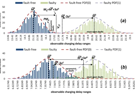
A. Handling uncertainty during DFT
We adapt the safe threshold computation and the observa-tion points selecobserva-tion to handle uncertainty. We assume 20% threshold voltage (Vth) and oxide thickness (tox) variations for all CMOS devices of the circuit. In Figure 12, we present the result of four Monte Carlo simulations with 500 permutations each, considering fault-free and single stuck-open faulty scenarios for two segment sizes L = 8 (Figure 12(a)) and L = 16 (Figure 12(b)) of the s38584 benchmark circuit. The ‘x’-axis is charging delay ranges and the ‘y’-axis reports the number of occurrences (bar) and their probability density functions (PDFs) (lines). The dark-shadedP DF(0) = [M0ij, σ
0
ij] belongs to the fault-free scenarios and the light-shaded P DF(1) = [M1ij, σ
1
ij] to the faulty ones. Note that RC parasitics are considered by the proposed PDN-aware DFT (Section IV) and that process variations could affect both PDN parasitics and the CMOS devices. However, PDN parasitics variations have negligible impact on the charging delay compared to CMOS devices variations, especially when the minimum distance between the SUT and the assigned observation point is constrained.
In Figure 12(a), the P DF(0) of the fault-free scenarios charging delay and the P DF(1) of the faulty scenarios do not overlap. This case is identified by the variations-aware safe threshold VST = (M
1
ij−3×σ
1
ij)−(M
0
ij + 3×σ
0
ij). Since it isVST >0, the overlap of the two PDFs is negligible. Note that a SUT, although it may be free from stuck-opens, it may suffer from parametric faults with charging delay similar to that of a stuck open scenario. However, we target stuck-opens and we consider the variation of the process parameters as fault-free by selecting the fault-free observable charging delay to be Mij = M
0
ij + 3×σ
0
[image:8.612.314.551.57.222.2]ij. Any parametric faults with higher charging delay than Mij are testable by this selection and a lower fault-free charging delay P Mij (shown in Figure 12) could be selected for parametric faults detection. After setting the fault-free charging delayMij, the observation points selection algorithm (Section IV-A3) is applied with
Fig. 12. Variations-aware safe threshold. (a)VST >0; (b)VST<0.
threholdST =VST. Heuristicsh1, h2 and h3 could be used
to identify the combination of observation pointDj and SUT
Si with the maximumσij values forVST computation. In Figure 12(b), the charging delays PDFs of the fault-free and the faulty scenarios overlap. This is also indicated by the negative VST value. The overlapping region belongs to fault-free scenarios, which exhibit high charging delay, due to process variations, that masks single stuck-open faults with low charging delay. A possible ad-hoc solution to avoid the overlapping region is the selection of a smaller segment size. However, a large SUT could be considered tolerant to stuck-open faults, if a faulty switch does not induce a higher charging delay than that of a fault-free SUT. Therefore, the fault-free charging delay is set at Mij = M
0
ij + 3×σ
0
ij. This way yield loss is avoided in exchange for fault coverage loss. However, a lower fault-free charging delay could be assigned for critical SUTs that are spatially closer to the longest paths. Also, since the safe threshold is negative, the observation points selection algorithm (Section IV-A3) is modified to select the clock edge that is closer to the Mij value. Next, we present the proposed calibration method to handle uncertainty due to unmodeled variations (Section V-B) and we present an approach to enhance test quality by handling systematic variations whenVST <0 (Section V-C).
B. Calibration for bridging model-to-silicon gaps
The proposed DFT method relies on SPICE simulations in order to estimate charging delays. However, due to model-to-silicon discrepancies [23], [24], SPICE simulations might be inaccurate compared to actual hardware measurements. Unconsidered PDN parasitics is a possible model-to-silicon discrepancy that could affect the PDN voltage level and the test quality. Therefore, we propose the post-silicon cal-ibration process shown in Figure 13. During this process, the calibration signal (Figure 11) exposes observation points output to the oscilloscope of the Automated Test Equipment (ATE) that collects the charging delay measurements. After the collection of an adequate measurements number, the post-silicon P DF(0) = [M0ij, σ
0
Fig. 13. Calibration method.
configuration (CF), which is the set of skip cyclesvariables
cij(Section IV-A3) for every group of SUTs is recomputed, by deploying the observation points selection algorithm (Section IV-A3) with the available on-chip observation points. The DFT is configured with CF, when it is set at test mode.
C. Handling of systematic variation
A practical approach is presented that increases the test quality of the proposed method under systematic variations (SVs) for large segment sizes withVST <0. Spatial correlated variations on the CMOS devices and parasitics of the PDNs are common between both inter-die and intra-die variability [25]–[27]. Systematic variations are explored by analysis of variance (ANOVA) [26], [27], a random to systematic varia-tion decomposivaria-tion technique by ranking candidate effects as possible sources of variation. For example, the wafer shown in Figure 13 is shaded according to the edge effect and the
center effect [27], two common sources of systematic spatial variability. The flow of this process is shown with dashed lines in Figure 13 together with the calibration flow. The calibration process jointly considers the collected measurements and the systematic variations to evaluate the calibration configuration. The systematic variations are used for clustering the SUTs and a calibration configuration is computed per cluster according to the discrepancies between each cluster’s charging delay mean. An example of this approach on spatial variations is demonstrated in Section VI-B.
Finally, note that the proposed method does not stress the chip at the corner cases of its thermal envelope [28] and temperature variability during testing is expected very low. However, if systematic temperature variations are observed during manufacturing testing by temperature sensors, they can be handled similarly to the case of systematic process variations by conducting clustering of charging delays based on discrepancies between the means of temperature variations.
VI. SIMULATIONRESULTS
In this section, we evaluate, through SPICE simulation, the performance of the proposed DFT architecture (Figure 11). We analyzed a large number of benchmarks from the IWLS’05 benchmark suite [19] and selected three representa-tives to present: theethernet(the largest of the IWLS’05), the
s38417 and the s38584circuits (the largest of the ISCAS’89 benchmarks included in the IWLS’05 suite). We consider
circuit setup |OP| OP-REG C-REG TAT (in ns) TQ
L×m R G R G R G R G
ethernet
16×128 1 1 7 7 110 30 16972 10556
TQ=100%
32×64 2 2 14 14 153 16 4812 2648 64×32 6 10 36 66 114 16 1316 652 128×16 9 9 45 45 30 10 388 172
s38417
8×64 2 2 7 28 48 18 524 498 16×32 4 5 42 42 21 16 174 176 32×16 2 3 10 14 20 8 54 56
64×8 3 1 20 3 12 3 16 8 128×4 2 2 4 4 2 2 4 4
s38584
8×64 4 2 8 14 27 36 572 527 16×32 9 11 77 40 14 14 131 120 32×16 3 8 15 6 12 5 44 32
64×8 3 4 16 3 6 3 12 8 128×4 2 2 4 2 2 2 4 4
the distributed PDNs model (Figure 3 and Table I) for both ring and grid power gating styles and various power switches segmentation setups. Also, for various parameters of the flow (Figure 7), we show the available trade-offs on test-application-time (TAT) and area cost. The operating frequency of all benchmarks was set atf = 1GHz.
A. Test quality and TAT evaluation
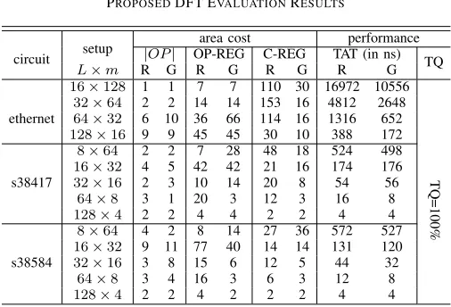
First, we present the results of the proposed method for various segmentation setups L×m for both ring and grid power gating styles for the three examined benchmarks. The parameterM OP (More Observation Points) is set to zero in order to trigger the selection of a minimum set of observation points. In Table IV, we present the area cost, in number of observation points |OP|, the size in flip-flops of the register file OP-REG that stores the observation point selection control data and the size of the register file C-REG that stores the skip cycles control data. The TAT and the TQ performance (without process variations) of the proposed method is also presented. The columns ‘R’ and ‘G’ belong to the ring and grid style, respectively. For the ethernet benchmark, the selected observation points number is in the range [1, 10] and [1, 9] for the grid and ring styles, respectively. The register files size (OP-REG + C-REG) is also very low, in the range [30, 82] and [33, 167] flip-flops for the grid and ring style, respectively. For all benchmarks and segmentation setups, the proposed method restores T Qto 100% when process variations are omitted.
Fig. 14. Fault coverage loss results for random and systematic variations.
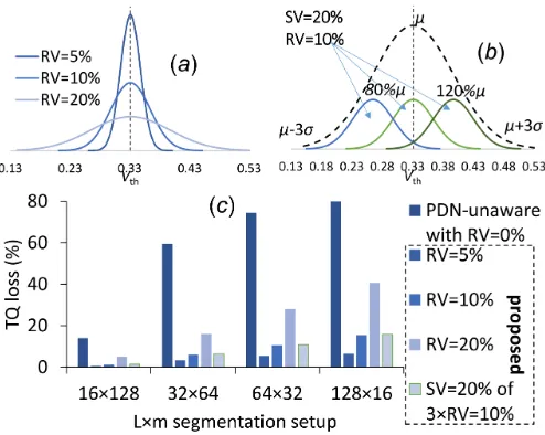
B. Test quality evaluation under process variations
[image:10.612.50.297.57.254.2]Next, we consider 5%, 10% and 20% process variations at the Vth andtox of the CMOS devices and we conduct Monte Carlo simulation of 500 permutations each. The variation for the Vth is shown in Figure 14(a). We also considered a case of systematic variations, shown in Figure 14(b). In that case we assume that the random variations of 20% has been decomposed to three components of systematic varations with 10% random variation each which is a possible outcome of analyzing, using ANOVA variation decomposition methods [26], [27], the spatial edge and center effects of wafer-to-die variability [27]. The wafer-to-dies in the wafer in Figure 13 have been shaded according to these effects. Figure 14(c) depicts the test quality loss ((TQ loss)=(false passes)+(false fails)) of the examined cases after applying the calibration method (Section V) on the ethernet benchmark for the examined segmentation setups L×m = 16×128,32×64,64×32 and 128 ×16. When the impact of PDNs is ignored and the testing is conducted through a random observation point with a constant capture moment for all SUTs and without considering process variations, we obtain the results shown with label “PDN-unaware with RV=0%”. By comparing these results with those of the proposed method that consider process variations, we conclude that the proposed PDN-aware DFT enables to minimize TQ loss even under process variations. Especially, for SUTs with small segment sizeL, the proposed method is tolerant on process variations. However, as expected, while L increases, test quality loss increases as well. For the case of L = 128, the TQ loss reaches 40.5% for 20% process variations. However even in that case, the TQ loss is 51.7% less than the TQ loss of the “PDN-unaware with RV=0%” method (83.9%). We note that the PDN-unaware method is evaluated without considering process variations (RV=0%). The proposed method does not suffer from yield loss due to the efficiency of the calibration method (Section V) under process variations. The yield loss noticed was less than 0.6%. However, it suffers from false passes in the range of
Fig. 15. Storage requirements for DFT control with and without compression.
[5%, 40.5%] whenRV = 20%based on the segment size L. Next we evaluate the ability of the proposed method to handle systematic variations. The results for 20% systematic process variation (case Figure 14(b)) are shown in Figure 14(c) with label “SV=20% of3×RV=10%”. The TQ loss (false passes) for that case drops (from [5%, 40.5%]) to the range of [1.4%, 19.7%], which is attributed to the efficiency of the calibration method to handle systematic variations. The TQ improvement compared to the PDN-unaware testing is in the range of 81.1% to 90% based on the segment size L, even when the PDN-unaware is evaluated with 0% process variations.
Note that the presented results consider process variations also at the NAND observation cells. Omitting the process vari-ations only at the observation cells, decreases the devivari-ations of the charging delays by 50%. Therefore, voltage monitoring alternatives, like those reported in [22], could be deployed as observation cells for more robust measurements.
C. Storage requirements and compression evaluation
Next, we evaluate the selection of RL compression for compressing the tests (tripletsSi,Dj,cij). Figure 15 depicts the storage requirements in number of flip-flops for storing the tests of the ethernet benchmark in uncompressed (triplets
Si, Dj, cij) and compressed (register files size C-REG+OP-REG) form for various setups L×m. Note that although only the SUTs number m is shown on x-axis, the size of a segmentLis given by L= 2048/m. As the SUTs number
m increases from m = 8 to m = 128, the uncompressed storage requirements increase from 80 to 1792 flip-flops. However, when RL compression is used, the compressed storage requirements increase slowly from 30 to 82 flip-flops in the range m = 8 to m = 32. For higher SUTs number m (m = 64 and m = 128), they decrease to 30 and 37 flip-flops, respectively. This is attributed to the higher observable charging delay of smaller SUT sizes L (L = 2048/m) that increases the range of compatible successive skip cycles, introduced in Section IV-A4. Therefore for higher SUTs number m, it is more frequent to select the same skip cyclescij between SUTs, which results to higher compression ratio. The achieved compression ratio of the RL compression
R = (uncompressed storage req.)/(compressed storage req.) is shown in Figure 15. It is alwaysR >1×and increases from
circuit
(ge) area (ge) area (%) area (ge) area (%) ethernet 157.5K 1015 0.64 643 0.41
s38417 30.5K 490 1.61 454 1.49 s38584 26.9K 611 2.27 435 1.62
D. Area cost evaluation
The proposed DFT architecture has the following area cost: area = (storage)+(control logic)+|OP|+|OP| ×1MUX. Table V presents the area cost for both ring and grid styles for the setups of Table IV with the highest hardware cost. Area cost is given in gate equivalents in column “area (ge)”. Column “area (%)” presents the relative area cost compared to the area cost of the circuit which is reported in column “size (ge)”. For example, for the ethernet benchmark of the grid style, the maximum storage requirements after compression (register files size OP-REG+C-REG) is obtained for the setup
L ×m = 64 ×32 and it is 82 flip-flops. Similarly, the highest control logic hardware cost for the ethernet is 280 gate equivalents. Specifically, this cost includes 4 counters for RL-decompression (CEC+OPC blocks), the SUTs counter, the FSM that coordinates the test application and a shift register of size m for asserting the sleepi signal of the SUT. One counter is for addressing the C-REG register file and it is of
log2(C-REG) bits size. The other one is for counting down
the successive SUTs that require the same skip cycles cij and its size is bounded bylog2(m). Similarly, another counter
is required for addressing the OP-REG register file and it is of log2(OP-REG) bits size. The last counter is for counting
down the successive SUTs that require the same observation point OPj and its size is also bounded by log2(m). Finally,
the observation logic requires |OP| observation cells and it is in the range [1, 10] NAND gates for the ethernet circuit. Therefore, for the case of the ethernet, the proposed method leads to 55%-68% area overhead compared to the state-of-the-art [15], which, however, is 0.41% the design size. The worst area overhead is 2.27% for the ring style of the s38584 circuit which is the smaller benchmark. Note that the relative area cost of the proposed method drops as the size of the circuit increases, clearly showing its scalability to large designs. We conclude that the proposed method achieves to restore T Q
with very low hardware overhead.
E. Trade-off between TAT and area cost
Next, Figure 16 presents a trade-off between hardware over-head and TAT for more observation pointsM OP = 3,4, . . .16 for the ethernet grid style setup of L ×m = 32 ×64. These values trigger the selection of more than the minimum
|OP| = 2 observation points. Both the TAT improvement and the hardware overhead are presented compared to the minimum observation points selection |OP| = 2. While the
[image:11.612.80.272.64.136.2]|OP|increases from 2 to 16, the storage requirements fluctuate in the range [30, 44] flip-flops, which is very low. Meanwhile, for M OP = 16, TAT decreases by 17% compared to the case of |OP| = 2, clearly indicating that more observation
Fig. 16. TAT vs. storage requirements by selecting more observation points.
points can be spared for less TAT, a trade-off observed in all simulations. Finally, note in Figure 16, how the value of
M OP = 10 is marked, as a pareto point, that minimizes the TAT with the minimum additional storage requirements.
VII. CONCLUSIONS
We showed that delay-based testing of power switches must consider a distributed model for the PDNs in order to avoid fault coverage loss and yield loss. To tackle this problem, we proposed a new PDN-aware DFT architecture (Figure 11), which is suitable for both ring and grid power gating styles. The DFT design flow (Figure 7) consists of practical heuristics (Section IV-A2) for scaling fault simulation requirements and an algorithm (Section IV-A3) that optimizes multiple objectives: test quality, TAT and area cost. The proposed method handles uncertainty (Section V-A) and can be calibrated (Section V-B) from post-silicon measurements. An approach to improve test quality when systematic variations are considered was also demonstrated (Section V-C). The simulation results show that the test quality which was lost due to PDNs is fully recovered (Table IV) and that 83.3% to 98.6% of the restored test quality is robust under process variations (Figure 14). A trade-off between area cost and TAT (Figure 16) has also been demonstrated. Finally, the proposed DFT requires minimum area cost (Table V) of less than 0.42% percent for a design with 157.5K gate.
ACKNOWLEDGMENTS
This work was supported by the Engineering and Physical Sciences Research Council, U.K., under Grant EP/K000810/1. The work of Dr. S. Khursheed was supported by the De-partment of Electrical Engineering and Electronics, University of Liverpool, U.K. The authors would like to thank Prof. Sudhakar M. Reddy (Iowa University) for his constructive feedback.
REFERENCES
[1] K. Roy, S. Mukhopadhyay, and H. Mahmoodi-Meimand, “Leak-age current mechanisms and leak“Leak-age reduction techniques in deep-submicrometer cmos circuits,” Proceedings of the IEEE, vol. 91, pp. 305–327, Feb 2003.
[2] X. Kavousianos and K. Chakrabarty, “Testing for socs with advanced static and dynamic power-management capabilities,” inProc. ACM/IEEE Des., Autom. & Test in Europe (DATE) Conf., pp. 737–742, March 2013. [3] J. Waicukauski and E. Lindbloom, “Failure diagnosis of structured vlsi,”
Design Test of Computers, IEEE, vol. 6, pp. 49–60, Aug 1989. [4] M. Abramovici, M. Breuer, and A. Friedman,Digital Systems Testing
and Testable Design. Piscataway, NJ, USA: IEEE Press, 1998. [5] S. Khursheed, B. Al-Hashimi, S. Reddy, and P. Harrod, “Diagnosis of
[6] D. Flynn, R. Aitken, A. Gibbons, and K. Shi,Low Power Methodology Manual: For System-on-Chip Design. NY, USA: Springer-Verlag, 2007. [7] C. Long and L. He, “Distributed sleep transistors network for power reduction,” inProc. Design Automation Conf., pp. 181–186, June 2003. [8] S. Khursheed, S. Yang, B. Al-Hashimi, X. Huang, and D. Flynn, “Improved dft for testing power switches,” in Proc. IEEE Eur. Test Symp., pp. 7–12, May 2011.
[9] S. Goel, M. Meijer, and J. de Gyvez, “Testing and diagnosis of power switches in socs,” inProc. Eur. Test Symp., pp. 145–150, May 2006. [10] P. Girard, N. Nicolici, and X. Wen, Power-Aware Testing and Test
Strategies for Low Power Devices. B¨ucher, Springer, 2010.
[11] H.-H. Huang and C.-H. Cheng, “Using clock-vdd to test and diagnose the power-switch in power-gating circuit,” in Proc. IEEE VLSI Test Symp., pp. 110–118, May 2007.
[12] S.-P. Mu, Y.-M. Wang, H.-Y. Yang, M.-T. Chao, S.-H. Chen, C.-M. Tseng, and T.-Y. Tsai, “Testing methods for detecting stuck-open power switches in coarse-grain mtcmos designs,” inProc. Intern. Conf. on Comp-Aid. Des., pp. 155–161, Nov 2010.
[13] Z. Zhang, X. Kavousianos, K. Chakrabarty, and Y. Tsiatouhas, “Static power reduction using variation-tolerant and reconfigurable multi-mode power switches,”IEEE Trans. Very Large Scale Integr. Syst., vol. 22, pp. 13–26, Jan 2014.
[14] R. Wang, Z. Zhang, X. Kavousianos, Y. Tsiatouhas, and K. Chakrabarty, “Built-in self-test, diagnosis, and repair of multimode power switches,”
IEEE Trans. Comput.-Aided Des. Integr. Circuits Syst., vol. 33, pp. 1231–1244, Aug 2014.
[15] S. Khursheed, K. Shi, B. Al-Hashimi, P. Wilson, and K. Chakrabarty, “Delay test for diagnosis of power switches,”IEEE Trans. Very Large Scale Integr. Systems, vol. 22, pp. 197–206, Feb 2014.
[16] V. Tenentes, S. Khursheed, B. Al-Hashimi, S. Zhong, and S. Yang, “High quality testing of grid style power gating,” inProc. IEEE Asian Test Symposium (ATS), pp. 186–191, Nov 2014.
[17] V. Tenentes, D. Rossi, S. Khursheed, and B. M. Al-Hashimi, “Diagnosis of power switches with power-distribution-network consideration,” 2015. [18] S. Zhong, S. Khursheed, and B. Al-Hashimi, “A fast and accurate process variation-aware modeling technique for resistive bridge de-fects,”IEEE Trans. Comput.-Aided Des. Integr. Circuits Syst., vol. 30, pp. 1719–1730, Nov 2011.
[19] IWLS’05 circts., online: http://www.iwls.org/iwls2005/benchmarks.html. [20] K. Chakrabarty, V. Iyengar, and A. Chandra,Test Resource Partitioning
for System-on-a-Chip. Springer US, 2002.
[21] Synopsys, “Dft compiler user guide: Scan,”SynopsysR, 2013. [22] R. Swanson, A. Wong, S. Ethirajan, and A. Majumdar, “Avoiding burnt
probe tips: Practical solutions for testing internally regulated power supplies,” inProc. IEEE Eur. Test Symp., pp. 1–6, May 2014. [23] B. Razavi, “Cmos technology characterization for analog and rf design,”
Solid-State Circuits, IEEE Journal of, vol. 34, pp. 268–276, Mar 1999. [24] A. Gattiker, M. Bhushan, and M. Ketchen, “Data analysis techniques for cmos technology characterization and product impact assessment,” inProc. IEEE Intern. Test Conf. (ITC), pp. 1–10, Oct 2006.
[25] B. Stine, D. Boning, and J. Chung, “Analysis and decomposition of spatial variation in integrated circuit processes and devices,”IEEE Trans. on Semicond. Manufactur., vol. 10, pp. 24–41, Feb 1997.
[26] A. Gattiker, “Unraveling variability for process/product improvement,” inProc. IEEE Intern. Test Conf. (ITC), pp. 1–9, Oct 2008.
[27] W. Zhang, K. Balakrishnan, X. Li, D. Boning, S. Saxena, A. Strojwas, and R. Rutenbar, “Efficient spatial pattern analysis for variation decom-position via robust sparse regression,”IEEE Trans. Comput.-Aided Des. Integr. Circuits Syst., vol. 32, pp. 1072–1085, July 2013.
[28] P. Tadayon, “Thermal challenges during microprocessor testing,”Intel Technology Journal, vol. Q3, pp. 1–8, 2000.
Vasileios Tenentes(M’07) is a Research Fellow at the ECS Department of University of Southampton, UK. In 2003, he received the B.Sc. degree in CS from the University of Piraeus in Greece, and in 2007 the M.Sc. degree in CS from the University of Ioannina in Greece. He worked at the R&D of Helic S.A. on EDA tools for embedded RF that were certified by TSMC. He obtained his Ph.D. in 2013 from the ECS of Ioannina University under an ESF scholarship. He has published 14 technical papers at refereed conferences and transactions of the IEEE.
Saqib Khursheed received his Ph.D. degree in Electronics and Electrical Engineering from Univer-sity of Southampton, Southampton, U.K., in 2010. Currently he is working as a lecturer (Assistant Professor) in the Department of Electrical Engi-neering and Electronics, University of Liverpool, UK. He is interested in all issues related to design, test, reliability and yield improvement of low-power, high-performance, multi-core designs and 3D ICs. He is the General Chair of Friday workshop on 3D Integration (DATE conference; 2013-), special session co-chair of European Test Symposium (ETS 2016-) and member of technical program committee of Asian Test Symposium (ATS 2015-), VLSI-SOC (2015-) and iNIS (2015-).
Daniele Rossi (M’02) received the Laurea degree in electronic engineering and the Ph.D. degree in electronic engineering and computer science from the University of Bologna, Italy, in 2001 and 2005, respectively. He is currently a Senior Research Fel-low at the University of Southampton, UK. His research interests include fault modeling and design for reliability and test, focusing on low power and reliable digital design, robust design for soft error and aging resiliency, and high quality test for low power systems.
Sheng Yang received the B.Eng. degree in Elec-tronic Engineering from University of Southamp-ton, UK, in 2008, and Ph.D. degree in Electronics Engineering from University of Southampton, UK., in 2013. In 2007 he did an internship with NXP modelling a data hub using systemC. In 2011 he held an internship with ARM investigating data integrity of flip-flops. Currently he is working as a post-doc research fellow in the School of Electronics and Computer Science, University of Southampton. His research interests include: low power and fault tolerance techniques for computer system through architectural design and runtime system management.
![Fig. 2. (a) DFT with lumped PDNs [15] and (b) stuck-opens test process.](https://thumb-us.123doks.com/thumbv2/123dok_us/8047730.222653/2.612.52.293.57.287/fig-dft-lumped-pdns-stuck-opens-test-process.webp)