Abstract:This paper proposes an analog-digital converter (ADC) using Single-electron transistor (SET).Single Electron Transistor is Nanodevice having a small quantum dot or island instead of the channel that works on the principle of Coulomb blockadewhich allows one electron tunnelingat a time from source to drain terminal. SET operates at low voltage and consumes lesspower. The proposed Flash ADC consists of SET based priority encoder and comparator circuits. The proposed design offers large input/output voltage swing, ultra-low power, compact circuit block for ADC compared to SET/CMOS hybrid amplifier-based ADC. In this paper, we have designed a 4-bit and 8bitFlash ADC using SET operating at room temperature and the performance estimationwas performed by using the CADENCE VIRTUOSO simulator.
Index Terms – Single Electron Transistor, Coulomb blockade, Analog-Digital Converter, Priority Encode,Comparator.
I. INTRODUCTION
Miniaturization has brought today’s electronic devices close to the size where quantum phenomena will dominate by changing the properties of the device.As CMOS technology nodes are scaling down, power consumption has become a primaryconcern for electronic system designs. Several low-power devices have been proposedto overcome this problem. One of the promising low-power devices is Single-Electron Transistor (SET) that can operate with low voltageat room temperature with only few electrons. These electrons are involved in the switching process, so SET suffers from less transconductance where we cannot achieve more gain [1,2]. The development of Ultra Low Power circuits promotes the analog-digital conversion (ADC) to achieve a directionof highspeed and low power dissipation. This paper is about the applications of the nanoelectronic device, i.e. ‘Single-electron transistor which is capable of controlling the transport of single electron from source to drain terminal and also provide on some essential device characteristics like Coulomb blockade. Single electron transistor exploits the quantum mechanical phenomenon of tunneling and it canperform as a switch or as an amplifier. XiaobinOuet al.[6] proposed two kinds of SET/MOS hybrid ADC and DAC circuits, which consist of SET, MOS transistors, and capacitors simulated using H-Spice simulator. Rathnakannanet al.[7] proposed three methods of Analog to Digital Conversion techniques for Eight-bit operation using Complementary Single Electron Tunneling
Revised Manuscript Received on July 05, 2019
Aarthy M, Department Of Micro & Nano Electronics, SENSE, Vellore Institute of Technology, Vellore -632014, Tamil Nadu, India
SriadibhatlaSridevi, Department Of Micro & Nano ElectronicsSENSE, Vellore Institute of Technology, Vellore -632014, Tamil Nadu, India
Transistor, Periodic Symmetric Function, SET/MOS hybrid using Single ElectronTransistor.
Choong Hyun Leeet al.[8] proposed Complementary single-electron transistor (SET)/CMOS hybrid amplifier based analog-to-digital converter with the combination of the amplification of SET current by MOSFETs and also suppress the Coulomb blockade oscillation current by increasing the island size, gate bias voltage and temperature.The conversion speed of ADC depends on the performance ofthe sample and hold block which could be improved by Hybrid SET a combination of SET and MOSFET, but the drawback is more power consumption [8].
Flash ADC requires a large number of comparatorscompared to other ADCs [9]. Hence, the increase in scaling, power consumption and cost of Flash ADC converters make the maintrade-off for many applications-oriented. Rahul et al.[9] proposed the low power Flash ADC designed with less number of low power consumption comparators. Mizugakiet al.[10] introduced4-bit flash ADC using single-electron signal modulator (SESM) with a capacitive voltage divider (CVD)also analyzed the characteristics of the CVD with stray capacitance. The signals from CVD are detected by SET and processed at quantizers as gray coded digital signals. In this paper,we proposedlow power 4-bit and 8-bit flash ADC using a single gate single electron transistor operating with low voltage at room temperature.
II. BACKGROUND
SET is a metallic-oxide-semiconductor field-effect-transistor (MOSFET), but with a small conducting island between source tunnel junctions and drain tunnel junctions. For the tunnel junctions composing the SET shown inFig. 1, the tunnel conductance is G1 and G2, the source tunnel junction capacitance is CSTJ and drain tunnel junction capacitance CDTJ, front gate capacitance C1 and back gate capacitance is C2 respectively. The drain, source, front gateandback gate voltage are VD, VS, VG1, and VG2, respectively. Both G1and G2 should be much smaller than 1/RQ, for the proper operation of the SET.RQ=h/e2 = 25.8kΩ quantum resistance or quantum conductance (G= 38.74μS).
This tunneling effect can be detected by a tunnel junction formed by two metallic electrodes separated by an insulating barrier. These three terminal switching nano devices can transfer electronsfrom source to drain one by one. Fig1 shows the schematic structure of SET.
A Low Power Flash ADC using Single-Electron
Transistor
Fig1.SET schematic
Fig 2.(a) and (b) shows the I-V Characteristics of the SET.The zero part of the curve indicates coulomb blockade where no electron tunneling takes place and as the bias voltage is applied, the electrons tunnel through the island from the source to the drain terminal.
Fig2.(a)
Fig2.(b)
Fig 2.(a) and (b) VI-Characteristic of single Electron transistor[SET]
In a single electron system, the tunnel junctions behave as a capacitor when an electron does not tunnel through them. Before any electron tunneling takes place, the island potential is given by equation(1) and (2) respectively.
V
island=
V
GS+
V
DS (1)= CG +CSTJ+CDTJ (2)
If weincrease the gate voltage VGS, thenVislandpotential becomes higher than e/2 so one electron can tunnel from the source terminal to the island. As aresult potential of the
island goes down by an amount of e/2 and
consequently,the voltage drop across the drain tunnel junction becomes higher than e/2 . Therefore one electron from the island can now tunnel out to the drain terminal and hence the original value of the island potential is once again
recoveredto enable one more electron to tunnel from the source terminal.
By increasing the channel width and the length of both the front gate and the back gate of SET, the Coulomb blockade region becomes narrower and the oscillation period of the drain current also decreases[3]. Also, by increasing the oxide thickness of both the front gate and the back gate of SET causes the Coulomb blockade region to become broader and increases the oscillation period of the drain current[3].For switching operation, the SET must be biased such that |VDS|
<
and at very high VDS such as when |VDS|
>
then VGS almost loses its control over ID and SET behaves like ordinary resistance.
III. FLASH ADC ARCHITECTURE
Analog to Digital Converters (ADCs) are the most vital devices, which convert analogsignal to digital signal.ADCs are used virtually everywhere, where analog signals have to be processed,storedor transported in digital form as0 and 1 and they are less susceptible to noise.The three fundamental ADC design parameters are speed, resolution and power dissipation. The conversion time is very fast for Flash ADC (or) parallel ADC than other types of ADCs such asSuccessive Approximation ADC, Dual SlopeADC and Sigma-Delta ADC.Flash ADCs consume more power, which could be overcome by using SET and are suitable for applications requiring huge bandwidth.
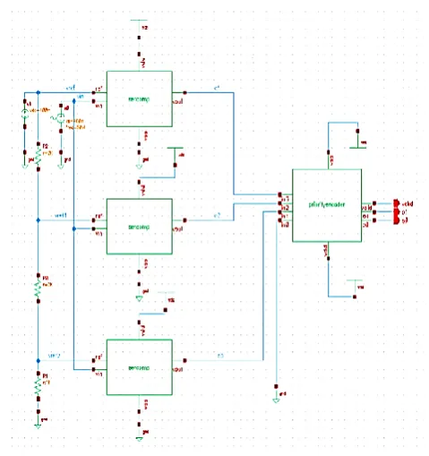
Fig 3 shows the block diagram of 4bit Flash ADC, which consists of 4:2 priority encoder, comparator and resistive ladder network. The analog signal is applied to the comparatorwherein the voltage level is divided by using a 2KΩ resistive ladder. The comparator outputis connected to the priority encoder to obtain the digital output.
Fig 3.Block diagram of 4bit FLASH ADC We designed and simulated the Flash ADC shown in Fig3 using SET based priority encoder and a comparator which operates at room temperature having lower power consumption and small gain error.
A. SET based 4- bit Priority Encoder Design
The priority encoder is used to compress the multiple binary inputs to less number of outputs. The design includes one inverter, one AND gate, three OR gate using single gate SET.Single gate SET works by applying input to gate1 and gate2 is grounded.The parameters used for modeling single gate SET C1=0.23aF, C2=0,
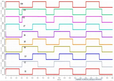
[image:2.595.312.536.464.592.2]simulation waveform is shown in Fig 5. Whenever d3 bit is high and rest other bits d0, d1, and d2 can be either 0or1 the output of priority encoder Out0 Out1 is high 11.
[image:3.595.53.284.97.537.2]Fig 4.SET based 4-bit priority encoder schematic
Fig 5.SET based 4-bit priority encoderoutput waveform
B. SET based 4- bit Flash ADC Design
[image:3.595.309.549.187.442.2]Here we design the priority encoder using single gate SET and a comparator circuit operating at room temperature with a minimum voltage of 0.4Vand improved switching activity because of the Coulombblockade effect. This architecture uses a dual power supply technique of VDD =400mV,VSS=-100mV to obtain the proper logic 0 and logic 1 condition. The comparator output is fed to the priority encoder to achieve the proper digital output.Thecomparator output is C3, C2, C1, and C0. The simulation waveform of the comparator and 4-bit Flash ADC is shown in Fig 7 & 8.
Fig 6. SET based 4-bit Flash ADC schematic
When Vin>Vref then comparator output becomes high (logic 1) else it is low (logic 0).So for supply voltage is 400mV, ifVin is 400mV and Vref is 400mV, so comparator output C3 is high. Finally, the output of the priority encoderO0 O1 is 11.
[image:3.595.55.281.570.747.2]Fig8.SET based 4-bit Flash ADC output waveform Similarly, we implemented 8-bit Flash ADC using single gate SET operating at room temperature. The simulation waveform of 8-bit priority encoder and 8-bit Flash ADC is shown in Fig 9 & 10.
Fig 9.SET based 8-bit priority encoder output waveform
Fig10.8bit Flash ADC output waveform
IV. PERFORMANCE ESTIMATION
ADC output is divided into 2Nuniform steps,each with width Δ. Any variation from the ideal step width is differential non-linearity (DNL)measured vertically (% or LSB).Where 1LSB = Vref/2N= 400mV/22 = 100mV.The measure of how closely the ADC output matchesits ideal response isIntegral non-linearity (INL)measured at each vertical jump (% or LSB).Fig 11 showsthe INL and DNL of the proposed set based ADC,respectively. Themaximum INL obtained is 0.3LSB and DNL is 0.5LSB.Table I shows the verification of proposed SET based Flash ADC with different parameters.
DNL
DIGITAL CODE
0 0.1 0.2 0.3 0.4 0.5 0.6
0 1 2 3 4 5 6 7
E
R
R
O
R
(
L
S
B
)
INL
DIGITAL CODE
-0.4 -0.3 -0.2 -0.1 0 0.1 0.2 0.3 0.4
0 1 2 3 4 5 6 7
INL
E
R
R
O
R
(
L
S
B
[image:4.595.49.292.54.220.2])
Fig.11 INL, DNL Parameters Existing
model[8]
Proposed Model
Resolution 4bit 8bit
Supply voltage 3V 0.4V
Input range 0V-5V 0.2-0.4V
DNL ±0.25LSB ±0.5LSB
INL ±0.25LSB ±0.3LSB
Power dissipation
6.2uW 2.56nW
Gain error 0.5% 0.2%
Temperature 77 K 300 K
Table I. Performance Comparison of various parameters of SET based Flash ADC
V. CONCLUSION
In this paper, we examined Flash ADC design using SET-based priority encoder and comparator. The proposed Flash ADC operates at room temperature which is achieved by adequately utilizing the Coulomb blockade effect of SET, with appropriate selection of
[image:4.595.55.285.289.452.2]circuit design, which exhibits large input-output voltage swing, low power and small gain error. This work could be extended for further optimization in terms of power and speed by using double gate SET and Hybrid SET a combination SET and MOSFET.
REFERENCES
1. K.K. Likharev, “Single-electron devices and their applications,” Proc,IEEE, vol. 87, no. 4, pp. 606 632, Apr.1999.
2. S. Mahapatra, V. Vaish, C. Wasshuber, K. Banerjee, and A. M. Ionescu, "Analytical Modeling of Single Electron Transistor for Hybrid CMOS SET Analog IC Design," IEEE Transaction Electron Devices, vol. 51, no. 11, pp. 1772–1782, Nov.2004.
3. KhadijehFeizi ,Saeed Haji Nasiri, “DC Characteristic Analysis of Single-Electron Transistor Based on MIB Model,”2010International Conference on Nanotechnology and Biosensors IPCBEE vol.2 (2011), Singapore.
4. DaeHwanKim, suk-Kang sung, KyungRokKim, jongduck lee,“single-electron transistors based on gate-induced si islandfor the single-electron logic application,” IEEE transactions on nanotechnology, vol. 1, no. 4, December 2002
5. Hu Chaohong, S.D.Cotofana, “Analog-to-digital converter based on single-electron tunneling transistors,” IEEEtransactions on very large scale integration (VLSI) systems, vol. 12, no. 11, November 2004. 6. XiaobinOu, Nan-Jian Wu, “Analog–digital and digital-analog
converters using single-electron and mos transistors,” IEEE transactions on nanotechnology, vol. 4, no. 6, November 2005.
7. K.Rathnakannan, P. VanajaRanjan, “Performance analysis of nanoelectronic single electron transistor based 8-bit a/d converters,”International Journal of Engineering and Technology, Vol. 5, No.1, 2008.
8. Choong Hyun Lee, Se Woon Kim, Jang Uk Lee, Seung Hwan Seo, Gu-Cheol Kang, Kang Sup Roh,Kwan Young Kim, Soon Young Lee, Dong Myong Kim, and Dae Hwan Kim, “Design of a Robust Analog-to-Digital ConverterBased on Complementary SET/CMOSHybrid Amplifier,”IEEE transactions on nanotechnology, vol. 6, no. 6, November 2007.
9. P.V. Rahul, Anusha A.Kulkarni, Sohail Sankanur, M.Ragavendra, “Reduced comparators for low power flash ADC using tsmc018,” in 2017 International conference on Microelectronic Devices, Circuits and Systems (ICMDCS)', IEEE, pp. 1-5.
10. Mizugaki, Y. & Delsing, P, “Single-electron signal modulator designed for a flash analog-to-digital converter,” Japanese Journal of Applied Physics 40(10R), 6157.
AUTHORS PROFILE
Aarthy Mis currently working as Assistant Professor at VIT University,Vellore.She has completed herM.E in VLSI design from Anna University, Chennai in 2012.She has completed her B.E in Electronics and Communication Engineeringfrom Anna University, Chennai in 2010.Her research interests include Digital IC design, Analog IC design, low power Nano IC design.
![Fig 2.(a) and (b) VI-Characteristic of single Electron transistor[SET]](https://thumb-us.123doks.com/thumbv2/123dok_us/8193728.258758/2.595.312.536.464.592/fig-b-vi-characteristic-single-electron-transistor-set.webp)