Rochester Institute of Technology
RIT Scholar Works
Theses Thesis/Dissertation Collections
11-1-2009
Analysis of a new modulation/ multiplexing
technique using mutually orthogonal chaotic
waveforms
Chaitanya Jidge
Follow this and additional works at:http://scholarworks.rit.edu/theses
This Thesis is brought to you for free and open access by the Thesis/Dissertation Collections at RIT Scholar Works. It has been accepted for inclusion in Theses by an authorized administrator of RIT Scholar Works. For more information, please [email protected].
Recommended Citation
DEPARTMENT OF ELECTRICAL ENGINEERING
KATE GLEASON COLLEGE OF ENGINEERING
ROCHESTER INSTITUTE OF TECHNOLOGY
ANALYSIS OF A NEW MODULATION/ MUTIPLEXING
TECHNIQUE USING MUTUALLY ORTHOGONAL CHAOTIC
WAVEFORMS
BY
CHAITANYA JIDGE
A THESIS
SUBMITTED TO THE DEANSHIP OF GRADUATE STUDIES IN PARTIAL FULFILLMENT OF THE REQUIREMENTS FOR THE DEGREE OF
MASTER OF SCIENCE IN
ELECTRICAL ENGINEERING
2
The people undersigned below read and accept the thesis work submitted.
Advisor:
______________________________
Dr. Chance M. Glenn Associate Dean of Graduate Studies
Rochester Institute of Technology Rochester, NY.
Committee Members:
______________________________
Dr. Andreas Savakis Head of Computer Engineering Department,
Rochester Institute of Technology, Rochester, NY.
______________________________
Dr. Tsouri Gill Electrical Engineering Department,
3
TABLE OF CONTENTS
TABLE OF CONTENTS ... 3
LIST OF TABLES ... 5
LIST OF FIGURES ... 6
ABSTRACT... 8
ACKNOWLEDGEMENT... 9
CHAPTER 1 - INTRODUCTION... 10
1.1 BACKGROUND ... 10
1.2 CHAOTIC PROCESS ... 11
1.3 CHAOTIC WAVEFORMS ... 14
1.4 LITERATURE REVIEW ... 16
1.4.1 QUADRATURE AMPLITUDE MODULATION (QAM)... 16
1.4.2 ORTHOGONAL FREQUENCY DIVISON MULTIPLEXING... 18
1.5 CHAOTIC WAVE MODULATION... 21
1.5.1 CHAOTIC COMMUNICATIONS... 23
1.5.2 SINGLE CHANNEL COMMUNICATION SCHEME BASED ON CHAOS………... 25
CHAPTER 2 - AN APPROACH TO A NEW MODULATION/ MULTIPLEXING TECHNIQUE... 27
2.1 FOURIER SERIES WAVE MODULATION (FSWM)... 27
2.2 MULTIPLEXING OF MUTUALLY ORTHOGONAL CHAOTIC WAVEFORMS (MOC)………. 29
2.2.1 SET OF CHAOTIC WAVEFORMS... 29
2.3 FORMULATION OF MOC COMMUNICATION SYSTEM ... 35
2.4. FORMULAE ... 39
2.4.1. HYBRID-A MOC... 39
2.4.2. FULL MOC ... 39
2.5 ERROR TERM CORRECTION ... 40
2.6 FULL MOC COMMUNICATION SYSTEM... 41
2.7 CONSTELLATION DIAGRAM OF MOC SYSTEM ... 48
4
2.8.1 FSWM... 50
2.8.2 HYBRID-A MOC AND FULL MOC ... 51
2.8 RESULTS ... 56
2.8.1 BER CURVES... 56
2.8.2 POWER SPECTRAL DENSITY ... 57
2.9 ANALYSIS... 60
CHAPTER 3 - CONCLUSION AND FUTURE WORK... 64
3.1 CONCLUSION... 64
3.2 FUTURE WORK... 64
5
LIST OF TABLES
Table 1. Mutually Orthogonal Chaotic Waveform Triplets Described By Their Variables... 31
6
LIST OF FIGURES
Figure 1. Circuit Diagram of Common Base LC Colpitts Oscillator [1]... 11
Figure 2. Plot of Variation in Emitter and Collector Voltages with Change in Inductor Current. ... 12
Figure 3. Plot of Inductor Current, Emitter Voltage and Collector Voltage [2]... 13
Figure 4. Formulation of a CCO Matrix. ... 15
Figure 5. Plot of Chaotic Waveform for the Described Values... 16
Figure 6. Block Diagram of QAM Modulator. ... 17
Figure 7. Block Diagram of QAM Demodulator... 18
Figure 8. Block Diagram of OFDM Communication System Modulator. ... 19
Figure 9. Block Diagram of OFDM Communication System Demodulator. ... 20
Figure 10. Block Diagram of Chaotic Modulation with Feedback [4]. ... 22
Figure 11. Plot of Chaotic Carrier, Auto Correlation Function and Power Spectral Density of CMFB [4]... 23
Figure 12. Block diagram of M-N FSWM Modulator... 28
Figure 13. Block Diagram of M-N FSWM Demodulator... 29
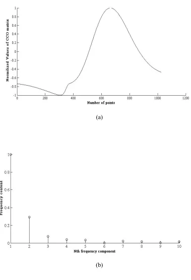
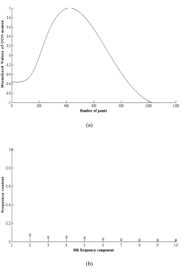
Figure 14. Chaotic Waveform 1(a) and Frequency Content (b) of the Waveform... 32
Figure 15. Chaotic Waveform 2 (a) and Frequency Content (b) of the Waveform... 33
Figure 16. Chaotic Waveform 3 (a) and Frequency Content (b) of the Waveform... 34
Figure 17. Result of Multiplexing Set of Chaotic Waveforms and Corresponding Frequency Content of the Waveform... 36
Figure 18. Block Diagram of Modulator for Hybrid-A MOC Communication System. ... 37
Figure 19. Block Diagram of Demodulator of Hybrid-A MOC Communication System... 38
Figure 20. Chaotic Carrier 1 (a) and Frequency Content (b) of the Chaotic Carrier... 42
Figure 21. Chaotic Carrier 2 (a) and Frequency Content (b) of the Chaotic Carrier... 43
Figure 22. Chaotic Carrier 3 (a) and Frequency Content (b) of the Chaotic Carrier... 44
Figure 23. Block Diagram of FULL MOC Transmitter. ... 46
Figure 24. Block Diagram of FULL MOC Demodulator. ... 47
(a). Transmitted Constellation Diagram. ... 49
(b). Received Constellation Diagram with a SNR=5dB. ... 49
7
Figure 26. FSWM Modulator Implemented Using Simulink. ... 50
Figure 27. FSWM Communication Implemented Using Simulink. ... 51
Figure 28. Implementation of MOC Communication System in Simulink. ... 52
Figure 29. Implementation of MOC Modulator in Simulink... 53
Figure 30. Simulink Implementation of MOC Demodulator... 54
Figure 31. FULL MOC Communication System in Simulink... 55
Figure 32. BER Curve for K=2 MOC Communication System. ... 56
Figure 33. BER Curve for K=3 MOC Communication System. ... 57
Figure 34. PSD Plot for K=2 MOC Communication System... 58
Figure 35. PSD Plot for K=3 MOC Communication System... 58
Figure 36. PSD Plot for K=4 MOC Communication System... 59
Figure 37. PSD Plot for FULL MOC Communication System... 59
Figure 38. BER Curves for MOC K=2, K=3... 60
Figure 39. BER Curve for 64-QAM. ... 61
8
ABSTRACT
A new digital modulation technique proposed [3] by Dr. Chance M. Glenn is presented
and analyzed in this report. The report explains the MOC algorithm as a means of creating
information-bearing baseband signals for modulation in digital communications. The process
uses the natural diversity of chaotic oscillations. An orthogonal triplet of waveforms is extracted
from the oscillations produced by a chaotic process. A simple digital communication system is
built, which uses this triplet as basis waveforms to formulate a baseband waveform.
There is a lot of research work done and still going on to use chaotic oscillations in the
communication system. The previously proposed communication systems have a disadvantage of
not retrieving the data back at the demodulator as the demodulator need to be synchronized with
the modulator, which cannot be implemented in real time.
We propose a new way of using chaotic oscillations. The work done and contribution
toward the thesis includes finding sets of mutually orthogonal chaotic waveforms using the data
collected from the various chaotic oscillations, finding an optimal set of chaotic waveforms that
can be used in the communication system. We demonstrated the implementation of the
communication system using Matlab and Simulink. We simulated and analyzed the
communication system built based on the MOC waveforms. We compared the results yielded
with other modulation schemes like QAM, QPSK. The goal is to show that the system
outperforms other comparable modulation/multiplexing techniques. We’ll use concepts such as
9
ACKNOWLEDGEMENT
During the course of my graduate studies and research, I had interactions with many
extraordinary individuals from whom I gained a lot of knowledge. Foremost, I thank my advisor
Dr. Chance M. Glenn for his guidance and support. His thought process and unique way of
implementing the ideas inspired me a lot.
I would like to thank my thesis committee members Dr. Tsouri Gill and Dr. Andreas
Savakis for being generous and cooperative.
I thank all faculty and staff of Electrical Engineering and Telecommunication
engineering technology Department for being nice and cooperative to me.
I am thankful to my parents and my brother, Krishna Jidge, for their support given to me.
10
CHAPTER 1 -‐ INTRODUCTION
1.1 BACKGROUND
The demand to transmit large chunks of data faster by more effective use of bandwidth is
growing. The wireless industry is shifting the standards from 3G to 4G, but the modulation
schemes for meeting the standards are the same modulation techniques used for 3G. There is a
disadvantage of using them as they require more bandwidth to achieve these standards. The
digital modulation techniques such as Quadrature Amplitude Modulation (QAM) and Quadrature
Phase Shift-Keying (QPSK) does not individually support high data rates transmission [5]. The
most effective methods of signal transmission used are Orthogonal Frequency Division
Multiplexing (OFDM) for its optimal bandwidth usage [21] and Multiple Inputs and Multiple
Outputs (MIMO) for its speed [5]. There has been a great deal of research work done and still
being done to devise a new modulation scheme using chaotic oscillations, but there are
difficulties in building a efficient demodulator as it needs to be synchronized with modulator to
demodulate the received signal and get the data back. We propose a new multiplexing technique,
which uses the inherent waveform shape diversity of chaotic oscillations to find sets of three or
more orthogonal waveforms. The orthogonal waveforms found are used to build a
11
1.2 CHAOTIC PROCESS
Generally, a chaotic process results from the action of a non-linear dynamical system
[10]. In a chaotic process, the state of the system depends on initial conditions. The chaos
process loses its deterministic nature over certain time and becomes undeterministic in nature. A
chaotic process looks similar to a random process, but a stationary random process is
independent of initial conditions while a chaos process is not. Looking at the process, one cannot
determine whether it is a random process, or a chaotic process. Some examples where we can
observe chaos processes are nature, chemical reactions, oscillation of pendulum, and electrical
circuits. The chaotic process has the ability to produce highly diversified waveforms and is
undeterministic in nature. Some examples of a chaotic process are Lorenz equation and Colpitts
oscillator [2].
[image:12.612.212.391.402.664.2]12
Figure 2 shows a common base Colpitts oscillator whose transistor is driven to non-linear
portion to show a chaotic process. The equations below describe the change in current, voltage at
emitter and at collector with respect to ground [2].
= − − +
(1)
= − −
(2)
= + −
(3)
= − −1 (4)
The corresponding plot shows the variation of the three variables , as
defined in the equations.
13
The nature of the plot is observed to be chaotic as a small change in initial conditions
resulted in a different path each time. This can also be explained as a small change in initial
conditions in which the variable takes a different path.
[image:14.612.118.484.184.471.2]14
1.3 CHAOTIC WAVEFORMS
The important characteristics of chaotic waveforms used are that the chaotic waveforms
generated by the chaotic oscillations are diversified in nature. This section deals with putting
together the chaotic processes described in the previous section to generate a huge Combined
Chaotic Oscillations (CCO) matrix. This CCO matrix is formulated from the output values of the
oscillations, which are used to form a chaotic waveform. The CCO matrix is used to search for
Orthogonal Chaotic Waveforms. Suppose we have multiple chaotic oscillators, where each one
may be multi-dimensional systems.
1, 2, 3, 4,…………, (5)
Each oscillation component can be described as
, (6)
where n is the component number. The z component of the Lorenz oscillation above may
be described as 23, .
We generated new sets of chaotic oscillations by combining these standard oscillations
together to create more complex forms
= 11, ,…, 1 , ,…., 1, ,…, , (7)
where nT is a type number. The CCO matrix which has 32 types of oscillations is
generated [2], with each holding 216 points in each type. Figure 4 shows a model CCO matrix.
The dimensions of the CCO matrix are 32 X 216. The process noted above generates a CCO
15
Figure 4. Formulation of a CCO Matrix.
The type (t), starting point (s) and number of points (Nc) are the variables defining the
chaotic waveform. These values of the waveform correspond to the row number, column number
,and number of values to be taken.
If the variable is defined as:
• t (type/row number) = 32;
• s (starting point/column number) = 40641;
• Nc (number of values/points) = 128;
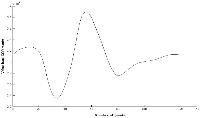
The corresponding chaotic waveform for the given values is plotted as shown in Figure 5.
The horizontal axis is the number of points in the chaotic waveform. The vertical axis is the
value. The values are extracted as 32nd row in CCO matrix, starting value is in column number
16
Figure 5. Plot of Chaotic Waveform for the Described Values.
1.4 LITERATURE REVIEW
This section deals with the research performed to devise a chaotic wave modulation in the
past as well as modulation techniques currently in use; for example, OFDM, QAM. Chaotic
wave modulation is the area of research from more than a decade. Communication systems built
using chaotic wave modulation has a similar disadvantage of not designing the demodulator,
which can be practically realized.
1.4.1 QUADRATURE AMPLITUDE MODULATION (QAM)
QAM is the simple and the most effective digital modulation technique. The name QAM
explains the complete modulation; that is, the amplitude modulation applied on waveforms
which are out of-phase. The communication system using QAM converts the digital data to
analog then placed on the in-phase and on the quadrature carrier and transmitted. The signal
received at the receiver is multiplied by the respective carrier to extract the baseband signal
[image:17.612.130.476.83.286.2]17
a QAM modulator. Figure 7 is the block diagram of QAM demodulator.
Figure 6. Block Diagram of QAM Modulator.
The number of bits encoded per symbol in an 2 -QAM is defined as:
= (8)
Bit-rate of QAM for a given symbol time ( ) is defined as:
=
(9)
Bandwidth efficiency or spectral efficiency of an M-QAM is:
[image:18.612.75.525.114.333.2]18
Figure 7. Block Diagram of QAM Demodulator.
1.4.2 ORTHOGONAL FREQUENCY DIVISON MULTIPLEXING
OFDM technique is the most efficient way of transmitting data. OFDM uses the given
bandwidth more efficiently as it uses multiplexing scheme to generate baseband waveforms.
OFDM takes in the data to be transmitted; converts it to digital data; divides the stream
according to the number of subcarriers; then places each piece of data on the subcarriers. Fourier
transformation is applied on these subcarriers to generate a baseband waveform then placed it on
the carrier and transmitted. The baseband signal is represented by equation (11) is for OFDM
with N subcarriers and M is the number of bits on each subcarrier.
= =0 −1 2 , 0≤ <
(11)
OFDM has edge over QAM, QPSK because of its better bandwidth efficiency. Usage of
multiplexing in modulation makes its advantageous as large data can be sent by using same
19
The output of transmitter is represented by following equation:
= (12)
Where frequency, T – symbol time and .
Figure 8 is the block diagram of OFDM transmitter. The equation (12) is output of the
block diagram. OFDM have an advantage of better bit rate with same bandwidth; that is, better
bandwidth efficiency
20
Figure 6 is OFDM demodulator, which receives the signal. The received signal is
represented by equation below
= + ( ) (13)
where N represents Additive white Gaussian noise (AWGN). The carrier signal
multiplies the received signal, filters it to eliminate the high frequency content, and transforms
the Fourier to obtain the data out from the received signal. The data is arranged to obtain the
transmitted signal back. OFDM can use M-QAM or QPSK or any modulation technique
according to the requirements to generate the baseband waveforms. OFDM is the most reliable
technique used for TV signal transmission under DVB-T standards [19]. OFDM is the most
efficient technique to use the given bandwidth [19].
21
1.5 CHAOTIC WAVE MODULATION
This section deals with some of the previous work performed on chaotic wave
modulation. There are numerous ways proposed to design a communication system using chaotic
wave modulation. The most common procedure for creating a transmitter is by using a
chua chaotic oscillator to generate chaotic waveforms. These are modulated by digital data
converted to analog data or which carry information; these waveforms are used to modulate the
carrier waveforms. Design of demodulator for the process is not perfect because chaotic
waveforms, which carry information, are random in nature making it difficult to design a
demodulator. These communication systems mentioned have an advantage because the
information sent is secure.
The chaotic wave modulation mentioned [4] below is chaotic modulation with feedback
(CMFB) to achieve synchronization. The binary message is multiplied by the chaos signal and
feed to the oscillator and transmitted. Figure 10 show that the receiver is mirror image to the
transmitter. The modulation scheme here has a large class of chaotic systems.
The transmitter is described by the following equations:
+1= + + − (14)
Where = ,
22
Figure 10. Block Diagram of Chaotic Modulation with Feedback [4].
The receiver system is driven by the following equations:
= + where is additive white Gaussian noise (AWGN).
+1= + + − (15)
Where =
The chaotic system was built according to the specifications given below:
=2.8−0.92.6−3.71.1−3.3−4.51.4−4.1, =110, =001
(16)
The results of the simulations are shown in Figure 11. The first graph is the chaotic
carrier; the second is the auto correlation function; and the last one is the power spectral density
[image:23.612.172.434.71.302.2]23
Figure 11. Plot of Chaotic Carrier, Auto Correlation Function and Power Spectral Density of CMFB [4].
There is disadvantage of the chaotic modulation scheme in that the receiver must be
synchronized with the transmitter. As a result, implementing it practically is not possible.
1.5.1
CHAOTIC COMMUNICATIONS
This section deals with various modulation schemes used in chaotic communications. In
traditional communication systems, the analogue sample functions sent through the channel are
weight sums of sinusoid waveforms and are linear [19]. However, in chaotic communication
systems, the samples are segments of chaotic waveforms and are nonlinear. This nonlinear,
unstable and a periodic characteristic of chaotic communication has numerous features that make
it attractive for communication use. It has wideband characteristic, it is resistant against
multi-path fading and it offers a cheaper solution to traditional spread spectrum systems [23]. Some of
the different modulation schemes used in chaotic communications are:
• Chaos shift keying (CSK)
• Differential Chaos shift keying (DCSK)
24
• Multiplicative Chaos Modulation (MCM)
In CSK each set of bits are mapped to different chaotic attractor. The information is
transmitted using attractor. The information received at the receiver contains noise and is
distorted and a decision is estimated from which attractor the waveform is produced and
is directed towards. Each attractor produces a function ( ) and the elements of the
signal set for i is given by equation below
= =1 , =1,2,…, (17)
The figure below is the block diagram of synchronized CSK demodulator.
Figure 12. Block diagram of Coherent Correlation Chaos Shift Keying (CSK) Receiver [23].
The signal ( ) received at the demodulator will try to synchronize all the chaotic
circuits in the receiver [23]. Generalized synchronization and Phase synchronization are the
different ways of synchronizing the chaotic circuits in the receiver.
25
1.5.2 SINGLE CHANNEL COMMUNICATION SCHEME BASED ON CHAOS
The communication system uses sinusoidal signals at different frequencies to put the binary
information to create baseband signals. The chaotic waveforms are used to put baseband signals
on the carrier signal. The mixed signal contains two separate chaotic carriers and two different
messages, serves as the only transmitting signal through the single channel for communication
[24]. This method has two chaotic oscillators at the receiver where one is called master oscillator
and the slave oscillator which is driven by master oscillator. The block diagram below represents
and explains the modulation scheme proposed based dual synchronization of colpitts oscillator.
Figure 13. Single-‐channel featured digital secure communication scheme [24].
The communication system uses OOK modulation scheme and there is no noise added to the
signal. The system is tested using binary data sequence ‘10101100’ and ‘11001010’. The signals
are generated and put it in chaotic carrier. The demodulated signal by the receiver and the
original signal transmitted are compared and shown in figure 15. The figure 14 explains the
[image:26.612.97.560.316.542.2]26
Figure 14. Chaotic Oscillator. (a)(b): at the master; (c)(d): at the slave after ideal channel; (e)(f): at the slave after AWGN channel [24].
[image:27.612.197.413.75.257.2] [image:27.612.227.406.328.537.2]27
CHAPTER 2 -‐ AN APPROACH TO A NEW MODULATION/
MULTIPLEXING TECHNIQUE
2.1 FOURIER SERIES WAVE MODULATION (FSWM)
FSWM is formulated using Fourier series decomposition of a waveform defined as:
= 0+ =1∞ 1 + 1 (18)
Where and are Fourier coefficient. These Fourier coefficients are generated in the
process of creating baseband signals. The general notation is M-N FSWM, where M helps in
defining the number of quantization levels and N is the number parts into which the in-phase data
is broken. The FSWM takes in the signal to be transmitted and divides it into in-phase and
quadrature signals. Then each part of the bit stream is divided into parts as defined by M and N.
The bits of information are used to generate a base band waveform by converting the digital
information to analog values. The analog information acts as coefficients in the equation (17)
and generates baseband waveforms. The generated base band waveforms are placed on the
carrier and transmitted. Figure 12 shows the block diagram of M-N FSWM modulator. The
number of quantization levels is given by the equation:
28
Figure 16. Block diagram of M-‐N FSWM Modulator.
The signal received at the demodulator is convoluted with the carrier and filtered to
extract the baseband signal. The data is extracted from the baseband signals by using the
equations 19 & 20.
=0 2
(20)
And
=0 ( ) 2
(21)
Where - Symbol time
The and are converted to bits of information by quantization. These bits are
arranged accordingly to get the transmitted data back. Figure 13 is the block diagram of M-N
29
Figure 17. Block Diagram of M-‐N FSWM Demodulator.
M-N FSWM works on the similar lines of OFDM. The advantages of multiplexing
orthogonal signals are studied in the process. A new multiplexing technique is proposed, which
uses the advantages of multiplexing to improve bandwidth efficiency and chaotic waveforms for
their resistance in the next section.
2.2 MULTIPLEXING OF MUTUALLY ORTHOGONAL CHAOTIC
WAVEFORMS (MOC)
2.2.1 SET OF CHAOTIC WAVEFORMS
Chaotic waveforms are the result of chaotic processes as explained in the previous
section. The diversified nature of chaotic waveforms is used to find orthogonal waveforms. This
part deals with how the sets of mutually orthogonal chaotic waveforms are formed and the
conditions for orthogonality between each waveform.
The first waveform is selected from the pool of low frequency waveforms having the
lowest second frequency component. The search process begins to find chaotic waveforms
30
The condition for orthogonality used and orthogonality factor (OF) between two
waveforms is represented by equation (21) below:
, =0 ≅0, ≠ (22)
If the orthogonality factor equals zero, then the two waveforms are called orthogonal
waveforms. When OF is approximately zero or near zero then the two waveforms are referred as
pseudo-orthogonal waveforms. Large number of sets of pseudo-orthogonal waveforms is put
together with the best pair of waveforms selected. These have combined lowest second to Nth
frequency content in them. Search for the third waveform is then on the conditions for the third
waveform in that the chaotic waveform is orthogonal to two other waveforms so these three
chaotic waveforms form a set of mutually orthogonal waveforms. The values in matrix are
explained as diagonal elements are dot product of same chaotic waveform by itself:
= . Where n = m (23)
and non-diagonal elements of the orthogonalization matrix are given by:
= . Where ≠ (24)
The orthogonalization matrix is represented by equation below:
= 11⋯ 1 ⋮⋱⋮ 1⋯
31
For the set of three mutually orthogonal chaotic waveforms the orthogonalization matrix
is given as:
= 11000 22000 33
(26)
The search results yielded many sets of mutually orthogonal waveforms.
Table 1. Mutually Orthogonal Chaotic Waveform Triplets Described By Their Variables.
Variables\set# 1 2 3 4 5 6 7 8 9 10 11
t1 16 20 30 1 1 1 3 4 6 6 6 6
s1 34753 18625 30785 6881 19553 57313 9057 64449 6881 8417 19553 32801
Nc1 128 128 128 256 256 256 256 256 256 256 256 256
t2 18 18 18 18 18 18 18 18 18 18 18 18
s2 37313 37313 37313 37313 37313 37313 37313 37313 37313 37313 37313 37313
Nc2 128 128 128 128 128 128 128 128 128 128 128 128
t3 30 30 30 30 30 30 30 30 30 30 30 30
s3 34977 34977 34977 34977 34977 34977 34977 34977 34977 34977 34977 34977
Nc3 128 128 128 128 128 128 128 128 128 128 128 128
The best set of waveforms is selected from the pool of sets of waveforms, which have
combined lowest second to Nth frequency content. The set of waveforms which have lowest
combined nth frequency component is presented below. This set of chaotic waveforms determines
32
(a)
(b)
[image:33.612.109.488.78.634.2]33
(a)
(b)
[image:34.612.114.485.86.630.2]34
(a)
(b)
[image:35.612.124.493.73.634.2]35
The orthogonalization matrix for the set of three chaotic waveforms used in the MOC
communication system is:
=498.7912.7950.1792.795441.4622.2430.1792.243438.928
(27)
If the chaotic waveforms are orthogonal, then the non-diagonal elements should be equal
to zero. The non-diagonal elements, however, are very small compared to the diagonal elements
and are near zero. This orthogonality is called as pseudo orthogonality. This pseudo
orthogonality adds up some errors while retrieving data. We propose an error correction
algorithm, which converge the estimation to the real data point at the demodulator side.
2.3 FORMULATION OF MOC COMMUNICATION SYSTEM
The set of waveforms selected from the previous section are used as basis functions for
the MOC communication system. MOC communication system uses the multiplexing technique
to combine the set of mutually orthogonal chaotic waveforms. The generalized way of
representing combined chaotic waveform of the set of is given by the equation:
= =1 (28)
When plotted below, the plot to the right is the frequency plot of the multiplexed chaotic
36
(a)
(b)
[image:37.612.127.490.86.630.2]37
The set of mutually orthogonal chaotic waveforms found are used as basis waveforms for
the MOC communication system to create baseband waveforms. The data to be transmitted using
MOC is sampled accordingly and converted to analog signal. This analog signal is used to
modulate the basis waveforms, which are multiplexed to form baseband waveform. The
generalized way of representing a baseband waveform is given by the equation below:
= 1 1+ 2 2+ 3 3 (29)
The equation (29) explains multiplexing of set of mutually orthogonal waveforms
1, 2, 3, which describes the function of block of MOC modulator block.
Figure 22. Block Diagram of Modulator for Hybrid-‐A MOC Communication System.
The carrier waveforms modulated by baseband waveforms are used to transmit
information. The in-phase and quadrature carrier are represented by equation (30) & (31):
= .∗ (30)
38
The transmitted signal is represented by equation (32):
= + (32)
The received signal is given by equation (33):
= + ( ) (33)
Where N - Additive White Gaussian Noise (AWGN).
Figure 23. Block Diagram of Demodulator of Hybrid-‐A MOC Communication System.
The baseband waveforms are extracted from carrier waveforms at the receiver. The data
can be extracted from baseband waveform by a standard demultiplexing method:
= 1. 1+ 2. 2+ 3. 3 (34)
1. = 1. 1. 1+ 1. 2. 2+ 1. 3. 3 (35)
The second term and third term of the equation will be equivalent to zero as the Ψ1 and
39
2.4. FORMULAE
2.4.1. HYBRID-‐A MOC
Number of bits per symbol is given by:
=6 (36)
Where K - number of bits on each chaotic waveform.
Bit-rate is number of bits per symbol divided by the symbol time:
= =6 (37)
Representing symbol time in terms of bandwidth:
=2 (38)
So, bandwidth efficiency is given by
= =3
(39)
2.4.2. FULL MOC
Number of bits per symbol is given by:
=9 (40)
40
Bit-rate is number of bits per symbol divided by the symbol time:
= =9 (41)
Representing symbol time in terms of bandwidth:
=2 (42)
So, bandwidth efficiency is given by:
= =4.5
(43)
2.5 ERROR TERM CORRECTION
The non-diagonal elements of orthogonality matrix are non-zero as they are
pseudo-orthogonal waveforms. The error correction algorithm is based on the dot product between any
of the two chaotic waveforms remains constant. In this case, the constant is a known value. This
error correction algorithm shifts the estimation of the data towards the actual data thus
minimizing the bit errors.
The process inside the demodulator is described by equation:
1. = 1. 1. 1+ 1. 2. 2+ 1. 3. 3 (44)
To get 1 back, the equation 39 is dotted with 2 to get 2 and dotted with 3 to get 3.
After getting m1, m2, m3. Then m2 is multiplied by dot product of 1and 2, m3 is multiplied by
dot product 1and 3and divided by 1. 1. The value obtained is subtracted from the m1
41
corrected in the similar way.
1= 1. 1. 1 (45)
12= 1∗ 12 11 (46)
13= 1∗ 13 11 (47)
The corrected m1 is written as:
1= 1− 12− 13 (48)
This reduces by the approximate value added during the process of demodulation. Thus,
the errors in the received data can be reduced.
2.6 FULL MOC COMMUNICATION SYSTEM
The Hybrid-A MOC communication system mentioned above in the previous section
uses the traditional sine and cosine as carriers. The FULL MOC communication system uses set
of mutually orthogonal chaotic waveforms as carriers. The set of mutually orthogonal waveforms
are different from the set of chaotic waveforms used for creating baseband waveform. The set of
waveforms used for carrier are searched through the chaotic waveforms using same procedure,
but made sure that they are orthogonal after the DC component is removed. The set selected has
the combined lowest second frequency component or that occupies less bandwidth. The chaotic
waveforms used as carriers in FULL MOC are mentioned in Figure a, b, and c. These waveforms
42
(a)
(b)
[image:43.612.120.489.75.600.2]43
(a)
(b)
[image:44.612.116.486.84.621.2]44
(a)
(b)
[image:45.612.120.492.81.648.2]45
The Transmitter of FULL MOC communication system receives the data to be
transmitted at the input port which takes number of bits at a time and divide it K bits of data
each which is to be placed on the mutually orthogonal waveforms in Figure 26 a, b & c by using
an digital to analog converter. The baseband waveform is generated by multiplexing the set of
modulated chaotic waveforms.
The general way of representing baseband waveform is given by equation (49).
= 1 1+ 2 2+ 3 3 (49)
Thus, the baseband waveforms are placed on the chaotic carriers, respectively, then
transmits information. The subcarrier is the result of convolution of baseband waveform (45) and
chaotic carrier given by the equation:
46
Figure 27. Block Diagram of FULL MOC Transmitter.
The output of the transmitter is represented as:
= =13 ( ) (51)
The received signal at the input of demodulator is combination of transmitted signal and
noise:
[image:47.612.92.513.72.433.2]47
Figure 28. Block Diagram of FULL MOC Demodulator.
The received signal is convoluted with the chaotic carriers and filtered to extract the
baseband signal. The baseband waveforms extracted at demodulator are represented as:
=∅ .∗ (53)
The baseband signal extracted is dotted with the set of mutually orthogonal chaotic
waveforms. The analog result is then converted to a digital value using a quantization technique.
The generalized way of representing the result is as:
= . (54)
The analog value is mapped to a digital value and un sampled to get the data back. Thus,
[image:48.612.91.511.70.311.2]48
2.7 CONSTELLATION DIAGRAM OF MOC SYSTEM
The signal constellation representation MOC for K=2 is shown in Figure 5. Each
16-point sub-constellation is independent of its neighbors. These 16-points represent the values of the
coefficients of chaotic waveforms. The coefficients from each of the in-phase combine to
generate the baseband waveform, while the in-phase and quadrature components produce two
different baseband waveforms. Each constellation point adds 4-bits of information to the bit
sequence; therefore we have a 12-bit sequence encoded in one symbol time. While the
constellation appears to be equivalent to 16-QAM, it is important to remember that each
sub-constellation is separate, and the voltage quantization levels used to specify the positions are
determined by the voltage range divided by four. For symmetric M-QAM, the voltage
quantization levels are determined by the square-root of M. For example, for 256-QAM, there
are 16 voltage quantization levels. The number of voltage quantization levels is directly related
to the amount of bit errors that will be induced by AWGN. This shows that MOC requires fewer
quantization levels for the same bandwidth efficiency, or that for the same number of
quantization levels MOC achieves higher bandwidth efficiency than QAM. The set of mutually
orthogonal waveforms has three waveforms in it. As a result, the constellation diagram has three
sets of 16-QAM equivalent constellation diagram. This explains it is three times faster than the
49
(a) . Transmitted Constellation Diagram.
(b). Received Constellation Diagram with a SNR=10dB.
[image:50.612.100.514.78.303.2]50
2.8 SIMULINK IMPLEMENTATION
Simulink is the software, which is a part of Math works matlab. Simulink gives a
reference to real time implementation.
2.8.1 FSWM
The FSWM is implemented using Simulink. The basic building blocks implement FSWM
in Simulink. The Bernoulli binary generator generates data to feed it to transmitter. The FSWM
uses blocks such as sine and cosine generators for generating carriers and for multiplexing and
demultiplexing blocks for arranging the data. Summation, product blocks perform addition and
multiplication of the input signals to the block. Low pass filter block is used in demodulator for
extracting baseband from carrier received. This may be controlled by describing the stop band
frequency. The gain block increases the strength of received signal at the demodulator. The
scope observes the output at a certain point.
[image:51.612.91.522.448.659.2]51
Figure 31. FSWM Communication Implemented Using Simulink.
2.8.2 HYBRID-‐A MOC AND FULL MOC
The MOC communication system is implemented using Simulink. Figure 32 shows
implementation of MOC communication system. Simulink has basic built-in blocks, which
function as they do in the real world. These blocks build the MOC system, simulating with
respect to time. Thus, the implementation in Simulink is a reference to implement it in hardware.
The data is generated using a Bernoulli binary generator, which can be set to a fixed bit-rate by
controlling the sample time of the block. The output of the bit generator is divided to two equal
[image:52.612.85.522.80.327.2]52
Figure 32. Implementation of MOC Communication System in Simulink.
Data is then demultiplexed to equal number of parts with each of value of K bits as
specified. The K number of bits is placed on each chaotic waveform of set of mutually
orthogonal waveforms by converting the digital data to analog and multiplying. Thus, the base
baseband waveform represented generally by equation (32) is the output of the MOC modulator
block. The next block is also a demux, which divides the bit stream into three parts of K bits
each. The digital data is converted to analog value by digital to analog converter block. The
chaotic waveforms are generated by block that gives a output matrix of dimensions defined by
Ns. The matrix is multiplied by value given by ADC block. This same procedure is applied to
other two streams with all the three values added by a sum block, which is the baseband
waveform. The baseband waveforms are multiplied by in-phase and quadrature carriers
generated by the sin and cosine generator blocks. The products are added by using a sum block
[image:53.612.88.523.77.362.2]53
Figure 33. Implementation of MOC Modulator in Simulink.
The transmitted signal is given to a block, which feeds to receiver without any physical
connection. The received signal is multiplied by the carrier waveforms generated by sine and
cosine generator blocks. The signal is filter using a low pass filter block defined by pass band,
stop band, attenuation, and max magnitude. The output of filter is the baseband extracted from
carrier at the receiver. The signal is buffered to Ns points, which are dotted by the basis
waveform to get the data where ADC block converts the analog value to digital data. The data is
[image:54.612.96.533.76.310.2]54
Figure 34. Simulink Implementation of MOC Demodulator.
The Full MOC system, which uses chaotic carriers instead of regular in-phase and
quadrature carrier, is implemented in Simulink. The carriers are generated repeatedly to make the
carrier continuous. This carrier is buffered using a buffer block, which buffers specified number
of input terms and gives a two dimensional output of row matrix of specified length. The MOC
modulator block generating baseband signals is the same from the regular MOC communication
[image:55.612.66.539.76.374.2]55
Figure 35. FULL MOC Communication System in Simulink.
[image:56.612.88.521.79.352.2]
56
2.8 RESULTS
2.8.1 BER CURVES
The MOC communication system is built as described using matlab and Simulink with
the results simulated. The BER results presented are simulated using matlab and the PSD plots
are simulated using Simulink. The BER curve is plotted by comparing the input data to the data
extracted; that is, output of the MOC demodulator. The number of errors divided by the total
number of bits gives us bit error ratio. The value of 0 may be observed when the BER curve
at bit error ratio equal to 10-6. The value is given as -10.5dB. The BER curve in figure 32 is for
MOC for value of K=2.
The 0 is given by equation:
0= −10 103 (55)
[image:57.612.112.503.419.672.2]57
The figure 37 is the BER curve for K=3 MOC communication system. The curve crosses
0 axis at -3dB for bit error ratio 10-6. The MOC K=3 is equivalent to 64-QAM in noise
performance from the levels of quantization. The error performance of MOC is better than QAM.
The curve is simulated using matlab and noise is Additive White Gaussian Noise (AWGN).
Figure 37. BER Curve for K=3 MOC Communication System.
2.8.2 POWER SPECTRAL DENSITY
The power spectral density plots are generated using Simulink. The PSD plots are
generated by performing FFT on the transmitted signal then averaged by number of points to
obtain a smooth PSD plot. The horizontal axis represents the frequency while the vertical axis
represents the power (magnitude square) units are dB. The plot in Figure 34 is for k=2 MOC
communication system. The PSD is plotted after the AWGN is added to the signal. The level of
noise in the signal is taken as 5dB. The bandwidth occupied at 2.4GHz center frequency and its
58
Figure 38. PSD Plot for K=2 MOC Communication System.
The plot in Figure 35 is for k=3 MOC communication system. The bandwidth occupied
at 2.4GHz center frequency and bit rate of 421.86Mbps is 600MHz.
[image:59.612.111.498.75.329.2] [image:59.612.89.499.430.652.2]59
The plot in Figure 36 is for k=4 MOC communication system. The bandwidth occupied
at 2.4GHz center frequency and bit rate of 562.48Mbps is 700MHz.
Figure 40. PSD Plot for K=4 MOC Communication System.
The PSD plot in the figure 37 is for FULL MOC communication system. The signal is
transmitted using chaotic carriers. The center frequency of operation is 3.4GHz.
[image:60.612.117.491.424.655.2]60
2.9 ANALYSIS
The results for MOC communication system and FULL MOC communication system are
simulated. This section deals with the comparison of results of MOC to the existing modulation
techniques like QAM. The figure 38 is the plot of BER curves for K=2, K=3 MOC.
Figure 42. BER Curves for MOC K=2, K=3.
The BER curve of QAM is simulated in matlab and the results are provided for
comparison. Table 2 compares the value of 0 at 10-6 BER for the QAM and MOC, which
operates at same bandwidth efficiency. The BER curve for K=2 MOC, which is equivalent to
64-QAM in bandwidth efficiency falls at -10.5dB. For K=3 MOC, the 0 value is -3dB, which
shows MOC has the better resistance to noise and the bit error rate at which K=2 MOC operates
is equivalent to 4096-QAM. The noise performance for K=2 MOC is equivalent to 64-QAM and
61
Figure 43. BER Curve for 64-‐QAM.
The BER curve for K=3 MOC crosses 0 -3dB compared to its equivalent 256-QAM
which has the same bandwidth efficiency crosses 0 at 22dB. The equivalent QAM in the bit
rate is 218-QAM which is very high. This comparison clearly shows the advantages of MOC.
Table 2. MOC Equivalent QAM.
MOC (Nbps) (calc.) (actual) Eb/N0 @
BER = 10-6
QAM*
(noise eq)
Eb/N0 @
BER = 10-6
K=2 (12) 6 ~4.5 -10.5dB 16 8dB
K=3 (18) 9 ~7 -3dB 64 22dB
K=4 (24) 12 ~9 4.5dB 256 35dB
[image:62.612.112.478.93.392.2]62
The K=2 MOC and 4096-QAM operates at 12 bits per symbol. Table 3 gives an
overview of MOC equivalent QAM in noise performance. The K=2 MOC is equivalent to
16-QAM as the from the constellation diagram for K=2 MOC its set of three 16-16-QAM’s. This is
same with the K=3, K=4 MOC. This is one more advantage of having a set of three mutually
orthogonal waveforms.
Consider the PSD plot for K=4 MOC system as shown in the Figure 34. The
specifications for the MOC simulations are given below.
The symbol time is taken as:
=4.2668 −9
Bit rate is calculated as:
=5.6248 9
Bandwidth occupied is given from the PSD plot for K=4:
≅700
The bandwidth efficiency of the system is calculated to be:
= =5.6248 9700 6≅8
The bandwidth efficiency clearly concludes the K=4 MOC operates at very high speeds
and still requires less bandwidth than the corresponding QAM, which needs more bandwidth for
its operations at higher bitrate. Thus, it can be stated that MOC communication system has an
63
[image:64.612.48.512.81.349.2]64
CHAPTER 3 -‐ CONCLUSION AND FUTURE WORK
3.1 CONCLUSION
In this thesis, the MOC communication system presented is designed using the inherent
waveform shapes generated by chaotic oscillations, which are highly diversified in nature. The
set of mutually orthogonal chaotic waveforms are searched for and found. The set of mutually
orthogonal waveforms are the basis waveforms for generating a baseband waveform. The MOC
is implemented using matlab and Simulink. The implemented model is tested with results
presented for K=2, K=3, and K=4 MOC communication system. The bit error rate, power
spectral density, and spectral efficiency of MOC are calculated, presented, then compared to the
present modulation schemes such as QAM.
The analysis of PSD plot presented is for K=4 MOC while the spectral efficiency is
calculated to be 8 then compared to its equivalent QAM. The MOC built using the set of
mutually orthogonal chaotic waveforms is much faster and more efficient than the present
modulation schemes.
3.2 FUTURE WORK
The MOC communication system is implemented in matlab and Simulink. The next step
is to implement MOC communication system using hardware and test it. Real time is then
compared. MOC communication system error performance, spectral efficiency with the existing
modulation techniques QAM. Search for triplet, which have less combined frequency content as
compared to the set of mutually orthogonal waveforms used in the MOC communication system
65
REFERENCES
[1]. C. M. Glenn, M. Eastman, and N. Curtis, “Digital Rights Management and Streaming of Audio, Video, and Image Data Using a New Dynamical Systems Based Compression Algorithm.” IADAT Conference on Telecommunications and Computer Networks, Conference Proceedings, September 2005.
[2]. C. M. Glenn, M. Eastman, and G. Paliwal, “A New Digital Image Compression Algorithm Based on Nonlinear Dynamical Systems”, IADAT International Conference on Multimedia, Image Processing and Computer Vision, Conference Proceedings, March 2005.
[3]. C. M. Glenn, J Chaitanya, “A New Multiplexing Technique Using Mutually Orthogonal Chaotic Waveforms”, (to be submitted) IEEE Transactions on Communications.
[4]. Feki M., Gelle G., Colas M., Robert B., Delaunay G., “Secure digital communication using chaotic modulation with feedback”. IEEE JNL 2005.
[5]. Jason Bellorado, Saeed Ghassemzadeh, Aleksandar Kavcic, “Approaching the Capacity of the MIMO Rayleigh Flat-Fading Channel with QAM Constellations, Independent across Antennas and Dimensions,” IEEE Transactions on Wi
![Figure
1.
Circuit
Diagram
of
Common
Base
LC
Colpitts
Oscillator
[1]](https://thumb-us.123doks.com/thumbv2/123dok_us/115866.11103/12.612.212.391.402.664/figure-circuit-diagram-common-base-lc-colpitts-oscillator.webp)
![Figure
3.
Plot
of
Inductor
Current,
Emitter
Voltage
and
Collector
Voltage
[2]](https://thumb-us.123doks.com/thumbv2/123dok_us/115866.11103/14.612.118.484.184.471/figure-plot-inductor-current-emitter-voltage-collector-voltage.webp)

![Figure
10.
Block
Diagram
of
Chaotic
Modulation
with
Feedback
[4]](https://thumb-us.123doks.com/thumbv2/123dok_us/115866.11103/23.612.172.434.71.302/figure-block-diagram-chaotic-modulation-feedback.webp)
![Figure
13.
Single-‐channel
featured
digital
secure
communication
scheme
[24]](https://thumb-us.123doks.com/thumbv2/123dok_us/115866.11103/26.612.97.560.316.542/figure-single-channel-featured-digital-secure-communication-scheme.webp)
![Figure
14.
Chaotic
Oscillator.
(a)(b):
at
the
master;
(c)(d):
at
the
slave
after
ideal
channel;
(e)(f):
at
the
slave
after
AWGN
channel
[24]](https://thumb-us.123doks.com/thumbv2/123dok_us/115866.11103/27.612.227.406.328.537/figure-chaotic-oscillator-master-slave-ideal-channel-channel.webp)