Keywords: High Voltage Direct Current transmission, Modular Multi-Level modeling, DC faults, voltage source converters
Abstract
At present High Voltage Direct Current (HVDC) Voltage Source Converters (VSC) are susceptible dc faults leading to extreme currents. The fault current cannot be controlled by the converter switching flows in the anti-parallel diodes. Protection devices are, therefore, required to operate with sufficient speed to avoid device failure. A method is introduced to calculate the critical time for protection to operate. Using this method it is then shown how the critical time may be extended by way of optimization of passive system components. In order to perform this optimization a new post-fault (when the converter gating signals are inhibited) model of the Modular Multi-Level (MMC) converter is introduced which drastically reduces simulation time, allowing high resolution parameter sweeps to be performed. The model is validated and is shown to produce fault characteristics similar to that of a conventional switched model.
1
Introduction
he use of voltage source converters (VSC) for HVDC transmission systems are becoming more widespread. They offer independent control of real and reactive power flow, unlike the ‘classic’ Line Commutated Converters (LCC), which is suited to the offshore wind applications, interconnections between weak networks or where rapid power reversal is required [1],[2].
Half bridge MMC, two level and NPC VSCs are all vulnerable to dc faults. When the dc side voltage collapses, the converter is no longer able to control power flow and current is drawn from the ac grid into the fault through its antiparallel freewheeling diodes (FWD). Converters employing full bridge cells such as full bridge MMC or hybrid cascaded two-level may be used to overcome this problem as they can block current in both directions[3]. However, the conduction losses and capital cost of the increased number of semiconductor devices make this approach less attractive[4],[5],[6].
The majority of VSC installations to date have been of the two-level type. This requires many devices to be connected in series in order to achieve the voltage blocking capability required, which is equal to the full DC link voltage.
This presents several problems for operation of the converter from the perspective of static and transient voltage sharing across so many series semiconductor devices(which limits switching frequency), and high dv/dt requires interfacing transformer with additional insulation requirements and electromagnetic shielding[8]. As the dc voltage increases this becomes more problematic and therefore somewhat limits the maximum voltage the two-level converters are able to operate at.
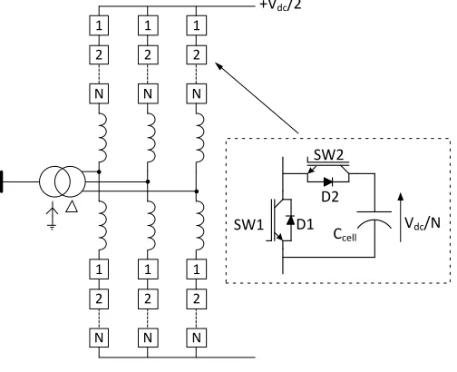
As power levels have increased, Modular Multi-Level Converters (MMC) are becoming more attractive over two-level and NPC converters[9]. The voltage output of each phase is a combination of many smaller steps from individual cells, see Figure 1. With a sufficient number of cells a near sinusoidal voltage output is attained with a low THD[5] eliminating filtering requirements. Switching losses are also reduced as staircase modulation can be used rather than high frequency pulse width modulation (PWM).
N 2 1 N 2 1
N 2 1 N 2 1
N 2 1 N 2 1
+Vdc/2
D1 SW1
D2
Ccell
SW2
[image:1.612.315.567.390.595.2]Vdc/N
Figure 1: Half-bridge MMC
There have been many publications recently investigating multi-terminal grids, HVDC faults, DCCBs and detection and protection strategies[6, 10-13]. However, there has been a lack of analysis on how the converter can be designed to optimize its performance during faults as well as normal operation which this paper attempts to address.
Current systems are constrained to point-to-point operation, with only two converters [7]. These systems rely on ac
DC Fault Parameter Sensitivity Analysis
Frederick Page, Grain Adam, Stephen Finney, Derrick Holliday, Lie Xu
protection in order to clear the fault and limit the damage to the converter and cables. With multi-terminal grids being proposed, much emphasis has been placed on developing a dc circuit breaker (DCCB)[6, 12]. It is equally important to give the same emphasis to adequately design converters that can deal with the fault currents that will be seen by its semiconductor switches, before standard ac protection operates. This is for several reasons:
Given the potential cost of (DCCB), it is likely that they will be used sparingly through a system and not necessarily at all converter terminals.
Although the likelihood is low it is still feasible that there is a bus bar fault that occurs before the dc breaker leaving it superfluous.
2
Point-to-point systems are unlikely to have
dc breakers installed, unless overhead line
(OHL) systems are to be used more
extensively as the likelihood of dc faults is
increased. Converter Parametric Analysis
To investigate the behaviour of an HVDC system when subjected to dc faults, a two terminal point-to-point, symmetrical monopole system is used, see Figure 2. No grounding is used on the DC side, thus, allowing the system to float during single pole-to-ground faults.VSC2 Grid 1
Grid 2
π
π
3Φ DC Line 3Φ
[image:2.612.315.544.205.406.2]DC Line VSC1
Figure 2: Point to point HVDC system
A Summary of the base system parameters used in this paper are given Table 1, which are taken from [14].
Table 1: HVDC System Parameters
Parameter Value
Rated power 1059MVA
Power factor ±0.95
DC Voltage ±320kV
Primary AC voltage 400kV Secondary AC voltage 333kV
DC line length 70km
Xtransformer 18%pu
Xarm 15%pu
Xeff 25.5%pu
Since the fault current through the converter is influenced by sizing of passive components it is therefore desirable to simulate systems being studied for a range of parameter values.
In this study, the ratio of arm to transformer inductance is varied, while the dc voltage, maximum modulation index,
converter PQ envelope, total effective impedance between converter and grid, and the transformer turns radio are kept fixed.
The effective impedance (Xeff) between the converter and the
point of common coupling can be expressed by: . (1)
Where, Xtrm and Xarm represent transformer and arm reactor per
unit impedances.. Figure 3 shows the possible combinations of arm and transformer impedance whilst keeping Xeff fixed at
[image:2.612.51.296.373.445.2]25.5%. Lower limits for the transformer and arm reactors impedances have been set to 10% and 5%..
Figure 3: Effective impedance to grid
Using the impedance constraint in Figure 3, it is possible to establish the correlation between the arm and transformer impedances and the overload semiconductors may experience by simulating combinations of impedances in dc faults. To achieve a reasonable resolution, 27 impedance pairs are defined along the line segment highlighted by the section shown in red in Figure 3.
2.1 DC fault severity Assessment
In MMC HVDC converters, the main components prone to failure during dc faults are the FWDs of the IGBTs that bypass the cell capacitor, when the converter is blocked. Exposure of these FWDs to increased current stresses for extended periods of time during dc faults may lead to device failure. A measure of energy absorbed found in manufacturers’ data sheets, generally referred to as i2t, is given by:
(2) In this paper i2t is used as an indicator of converter failure.
When the measured i2t of a given device exceeds its specified
limit given by the data sheet, converter damage is expected. The estimated time period between the fault initiation and damage occurring can be used as a guideline to set the critical time for protection (ac/dc circuit breakers or otherwise) in order to avoid converter failure. However, the critical fault
0 10 20 30 40 50
-5 0 5 10 15 20 25 30
Xarm [%pu] X trm
[
%
pu
]
[image:2.612.80.266.513.642.2]clearing time must take into broader system prospective such as stability of the both ac systems of the HVDC link.
Through appropriate design of system inductances it may be possible to modify the dc fault profile, reducing stress on the FWDs and increasing the time available for protection systems to operate.
Detailed parametric analysis requires large numbers of simulations to be carried out. Performing such studies using a conventional MMC switching model is processor and time intensive. This paper presents a simplified model of the MMC that can accurately represent the converter post-fault, when gating signals are inhibited.
3
Diode Model Validation
MMC converters generally consist of many hundreds of cells and in conventional models each of these would be modeled at the switch level. As the number of voltage levels increases so does the number of cells, and therefore the complexity of the model. The capacitor voltage measurement of each cell is required in order to carry out capacitor voltage balancing within the arm, and to generate the gating signals that control which cells to be switched ‘on’ within each sampling time. The large number of measurements, control signals, and complexity of the power circuit lead to long simulation times. To address this, several modeling techniques have been proposed already [15-17]. However, the reduction achieved with techniques presented in [15-17] is not sufficient to perform a large number of simulations efficiently. Therefore, the following subsection explains a reduced complexity model of the MMC introduced in this paper to facilitate a large number of simulations efficiently when performing dc fault analysis.
3.1 Diode model
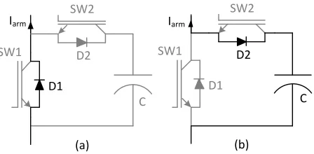
When a dc fault occurs, the current within the cells rises rapidly causing the IGBTs within the cells to be gated off almost immediately. At this point, the IGBTs no longer form part of the current carrying circuit. The only conduction paths are through the FWDs. The current flow from the ac to dc side and vice versa is depicted in Figure 4.
D1
SW1 D2
C SW2
D1
SW1 D2
C
SW2
(a) (b)
Iarm
[image:3.612.313.567.156.290.2]Iarm
Figure 4: Diode model cell equivalent circuit for (a) positive current (b) negative current
When all the IGBTs are gated off and iarm<0, the current in an
individual cell must flow through diode D2 and the cell capacitor. This allows the capacitors of the series cells in each
arm to be combined into a single composite capacitor, with capacitance of (Ccomposite=Ccell/n), and where the components
are scaled accordingly. When iarm>0, current must flow
through diode D1 in each individual cell. The current in all
cells must be in the same direction as the IGBTs are inhibited. The diode model is produced by replacing the string of series cells in each arm with a single cell where IGBTs are replaced with diodes, as shown in Figure 5.
3Φ
L1 L3 L5
L2 L4 L6
D2
C/N D1
Figure 5: Diode Model
The proposed diode model is validated against a switching MMC model, with 21 cells per arm, where all basic HVDC controllers are incorporated. The 21-cell model is initially run up to full power flow conditions, with VSC1 controlling power
flow and VSC2 controlling dc voltage. Power flow is from
VSC1 to VSC2.
When the system has reached steady state condition, a dc fault is initiated at the centre point of the dc line, 35km from either converter. A more detailed analysis of dc faults may be found in [18].
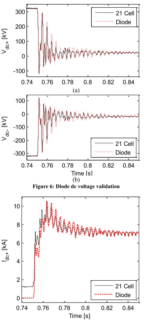
3.2 Model comparison
A pole-to-pole fault is initiated at time t=0.75s, and gating signals are inhibited 1ms after fault initiation within the 21 cell model. The initial dc voltage within the diode model is set using fixed dc voltage sources to pre-charge the line capacitances, until the point at which the fault is applied when they are switched out. Figure 6 shows the positive and negative dc voltage, measured at the terminals of VSC1.
Observe that the diode model closely follows the 21 cell model. The dc voltage rapidly collapses to zero on both the positive and negative poles.
Figure 7 shows the dc current from the positive pole to VSC1
[image:3.612.58.282.540.650.2](a)
[image:4.612.49.283.54.575.2](b)
Figure 6: Diode dc voltage validation
Figure 7: Diode dc current validation
The upper arm currents of VSC1 are given in Figure 8(a) for
the diode and 21 cell model. The 21 cell model clearly shows balanced three phase arm currents prior to the fault at t=0.75s, whereas the current in the diodes model is zero, as expected. When the fault is initiated current rises in the arms (and therefore diodes) as it is drawn in from the grid. The current in the diodes can be seen to correlate well with that of the 21 cell switching model.
The lower arm currents can be seen in Figure 8 (b) show the lower arm current within VSC1. Again the diode and 21 cell
model currents match well. There is a disparity in the first
peak of phase C, in line with the magnitude of current present prior to the fault.
(a)
[image:4.612.314.544.75.438.2](b)
Figure 8: Diode arm current validation
The ac current measured at the converter side of the transformer at VSC1 is shown in Figure 9. The diode and 21
[image:4.612.319.543.505.675.2]cell models again show good correlation once the fault is initiated.
Figure 9: Diode ac current validation
Table 2 summarises the performance differences between the two models. For each model the simulation is left to run for 150ms post-fault in order to capture the resulting waveforms.
0.74 0.76 0.78 0.8 0.82 0.84
-100 0 100 200 300
V dc
+
[
kV
]
21 Cell Diode
0.74 0.76 0.78 0.8 0.82 0.84
-300 -200 -100 0 100
Time [s] V dc
[
kV
]
21 Cell Diode
0.74 0.76 0.78 0.8 0.82 0.84
0 2 4 6 8 10
Time [s] I dc+
[
kA
]
21 Cell Diode
0.74 0.76 0.78 0.8 0.82 0.84
0 2 4 6 8 10
I abc
[
kA
]
0.74 0.76 0.78 0.8 0.82 0.84
0 2 4 6 8 10
Time [s] I abc
[
kA
]
Ia21
Ib21
Ic21
IaD
IbD
IcD
0.74 0.76 0.78 0.8 0.82 0.84
-6 -4 -2 0 2 4 6
Time [s] I abc
[
kA
]
Ia21
Ib21
Ic21
IaD
IbD
Table 2: Model Performance Summary
21 Cell Diode
Time to initiate 0.75s 20ms
Total simulation time 0.90s 170ms
Real time per ms of
simulation time 2.18s 0.013
Real time for single fault case
1967s = 33m 2.0s Real time for 27 case
analysis 53109s = 14h45m 54s
The difference in simulation times clearly demonstrates the models advantage when performing large amounts of simulations. This offers users the ability to perform large sweeps of parameters with high resolution between data points whilst maintaining a high degree of accuracy.
The diode model has been shown to produce simulation results similar to that of the 21 cell switching model. The error within the first cycle is approximately equal in magnitude to the initial current in the 21-cell switching model. The validation plots (Figure 6 - Figure 9) also demonstrate that the main contribution of fault current is independent of initial conditions.
4
Simulation Results
Given the number of simulation cases required to perform a parametric analysis as set out in section 2, the diode model is used for the analysis to produce the following results.
4.1 Calculation of i2t
Table 3 shows the ratings of a range of devices that are suitable for the converter specification. The i2t ratings of three
devices (520kA2s, 720 kA2s and 911 kA2s) are now used to set
the threshold within the simulations.
Table 3: Common IGBT ratings
Manufacturer Nominal rating Vce Surge rating [V] Ic [A] Ipeak [A] ∫i2dt [kA2s]
Semikron[19] 1200 1500 10200 520
ABB[20] 3300 1500 13500 911
ABB[21] 1700 2000 12000 720
Infineon[22] 3300 1500 12080 730 Dynex[23] 3300 1500 12000 720
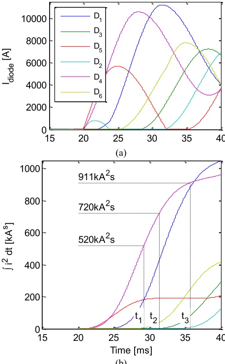
Figure 10 (a) shows the snapshot of the diode currents of all six arms during a pole to pole fault at the terminals of VSC1,
zoomed around the first fundamental cycle following fault initiation.
For each diode the running sum of the trapezoidal integration of i2t is taken. As the current is unevenly in the diodes this
leads to uneven distribution of i2t as can be seen in Figure
10(b). The time to exceed the threshold for each of the three i2t
ratings is measured as shown in Figure 10(b).
In this case t1 =9.22ms, t2 = 11.35ms and t3 = 15.7ms after the
fault is initiated.
(a)
(b)
Figure 10: Calculation of i2t from diode currents
4.2 Parametric analysis
[image:5.612.50.298.53.169.2]The same evaluation is now performed for the 27 impedance pairs. Figure 11 shows the time taken to reach thresholds as the ratio of arm inductance to transformer inductance is altered (where Xeff is fixed).
Figure 11: Variable arm and transformer inductance
15 20 25 30 35 40
0 2000 4000 6000 8000 10000
I diod
e
[
A
]
D1 D3
D5
D2 D4 D6
15 20 25 30 35 40
0 200 400 600 800 1000
i
2 d
t
[k
A
s ]
Time [ms] 520kA2s
720kA2s 911kA2s
t1 t2 t3
0.5 1 1.5 2 2.5 3
10 15 20 25 30
Ratio of Xarm/Xtrm
T
im
e
to
r
ea
ch
i
2 dt
li
m
it
[m
s] 520kA2s
[image:5.612.320.543.506.695.2]The results in Figure 11 demonstrate that placing a larger proportion of Xeff in the arms tends to improve withstand of the
MMC FWDs against pole-to-pole dc faults. Thus, MMC FWDs are expected to survive for longer period compared to the cases when the majority of impedance is placed in transformer. For the range of parameters simulated here an increase of approximately 15ms is gained by letting the transformer reactance go down to its lower limit of 10% and increasing arm reactance to 31%.
5
Conclusions
The diode model has been shown to provide results that are in line with that of a 21cell switching model. The advantage of which is primarily of its increased speed, which lends itself to tasks where a high number of repetitive simulations are required, such as the parametric analysis shown.
There are two ways in which the diode model can provide this increase in speed over its detailed counterpart. Firstly the model takes only a short period to achieve a steady state condition before the dc fault can be applied. The second part is provided by the reduced complexity of the model. The diode model has only six diodes in each converter verses the 126 diodes and 126 switches in the 21cell model. There are also no controllers. This leads to the 21-cell model taking a significantly longer real time to process each ms of simulation time.
The trade-off between placing the system reactance in the transformer or arms shows, for fault performance, it is desirable to favour the arm inductors. A more detailed study is required to assess the impact of this in a more general sense on system performance. Unlike the transformer the arm inductors carry a dc current component which may lead to difficulties in design and manufacturing.
6
References
[1] Z. Lidong, L. Harnefors, and H. P. Nee, "Interconnection of Two Very Weak AC Systems by VSC-HVDC Links Using
Power-Synchronization Control," Power Systems, IEEE
Transactions on, vol. 26, pp. 344-355, 2011.
[2] J. Dorn, M. Pohl, D. Retzmann, and F. Schettler, "Transformation of the Energy System in Germany - Enhancement of System Stability by Integration of
innovative Multilevel HVDC in the AC Grid," in Security in
Critical Infrastructures Today, Proceedings of International ETG-Congress 2013; Symposium 1:, 2013, pp. 1-6.
[3] G. P. Adam, S. J. Finney, and B. W. Williams, "Hybrid converter with ac side cascaded bridge cells against H-bridge alternative arm modular multilevel converter:
steady-state and dynamic performance," Generation, Transmission
& Distribution, IET, vol. 7, pp. 318-328, 2013.
[4] D. Soto-Sanchez and T. C. Green, "Control of a modular multilevel converter-based HVDC transmission system," in Power Electronics and Applications (EPE 2011), Proceedings of the 2011-14th European Conference on, 2011, pp. 1-10.
[5] C. C. Davidson and D. R. Trainer, "Innovative concepts for hybrid multi-level converters for HVDC power
transmission," in AC and DC Power Transmission, 2010.
ACDC. 9th IET International Conference on, 2010, pp. 1-5.
[6] W. Yeqi and R. Marquardt, "Future HVDC-grids employing modular multilevel converters and hybrid DC-breakers," in Power Electronics and Applications (EPE), 2013 15th European Conference on, 2013, pp. 1-8.
[7] C. M. Franck, "HVDC Circuit Breakers: A Review
Identifying Future Research Needs," Power Delivery, IEEE
Transactions on, vol. 26, pp. 998-1007, 2011.
[8] H. Weiwei, P. Palmer, Z. Xueqiang, M. Snook, and W. Zhihan, "IGBT series connection under Active Voltage
Control," in Power Electronics and Applications (EPE
2011), Proceedings of the 2011-14th European Conference
on, 2011, pp. 1-9.
[9] L. G. Franquelo, J. Rodriguez, J. I. Leon, S. Kouro, R. Portillo, and M. A. M. Prats, "The age of multilevel
converters arrives," Industrial Electronics Magazine, IEEE,
vol. 2, pp. 28-39, 2008.
[10] M. Hajian, D. Jovcic, and W. Bin, "Evaluation of Semiconductor Based Methods for Fault Isolation on High
Voltage DC Grids," Smart Grid, IEEE Transactions on, vol.
4, pp. 1171-1179, 2013.
[11] M. K. Bucher and C. M. Franck, "Contribution of Fault Current Sources in Multiterminal HVDC Cable Networks," Power Delivery, IEEE Transactions on, vol. 28, pp. 1796-1803, 2013.
[12] C. Meyer, M. Kowal, and R. W. De Doncker, "Circuit breaker concepts for future high-power DC-applications," in Industry Applications Conference, 2005. Fourtieth IAS Annual Meeting. Conference Record of the 2005, 2005, pp. 860-866 Vol. 2.
[13] T. Lianxiang and O. Boon-Teck, "Locating and Isolating
DC Faults in Multi-Terminal DC Systems," Power Delivery,
IEEE Transactions on, vol. 22, pp. 1877-1884, 2007. [14] J. Peralta, H. Saad, S. Dennetiere, J. Mahseredjian, and S.
Nguefeu, "Detailed and Averaged Models for a 401-Level
MMC–HVDC System," Power Delivery, IEEE
Transactions on, vol. 27, pp. 1501-1508, 2012.
[15] U. N. Gnanarathna, A. M. Gole, and R. P. Jayasinghe, "Efficient Modeling of Modular Multilevel HVDC
Converters (MMC) on Electromagnetic Transient
Simulation Programs," Power Delivery, IEEE Transactions
on, vol. 26, pp. 316-324, 2011.
[16] X. Jianzhong, Z. Chengyong, L. Wenjing, and G. Chunyi, "Accelerated Model of Modular Multilevel Converters in
PSCAD/EMTDC," Power Delivery, IEEE Transactions on,
vol. 28, pp. 129-136, 2013.
[17] H. Saad, J. Peralta, S. Dennetiere, J. Mahseredjian, J.
Jatskevich, J. A. Martinez, et al., "Dynamic Averaged and
Simplified Models for MMC-Based HVDC Transmission
Systems," Power Delivery, IEEE Transactions on, vol. 28,
pp. 1723-1730, 2013.
[18] Y. Jin, J. E. Fletcher, and J. O'Reilly, "Short-Circuit and Ground Fault Analyses and Location in VSC-Based DC
Network Cables," Industrial Electronics, IEEE Transactions
on, vol. 59, pp. 3827-3837, 2012.
[19] Semikron, "SKiiP 1513 GB172-3DFW V3 Datasheet," Semikron, 2012.
[20] ABB, 5SNA 1500E330305 Datasheet, 2013.