Rochester Institute of Technology
RIT Scholar Works
Theses Thesis/Dissertation Collections
6-1-2009
High-performance subthreshold standard cell
design and cell placement optimization
Sumanth Amarchinta
Follow this and additional works at:http://scholarworks.rit.edu/theses
Recommended Citation
High-Performance Subthreshold Standard Cell Design and
Cell Placement Optimization
by
Sumanth Amarchinta
A Thesis Submitted in Partial Fulfillment of the Requirements for the Degree of Master of Science in Computer Engineering
Supervised by
Dr. Dhireesha Kudithipudi Department of Computer Engineering
Kate Gleason College of Engineering Rochester Institute of Technology
Rochester, New York June 2009
Approved By:
Dr. Dhireesha Kudithipudi
Assistant Professor, Department of Computer Engineering Primary Advisor
Dr. James Moon
Associate Professor, Department of Electrical Engineering
Dr. Ken Hsu
Dedication
Acknowledgments
I sincerely thank my advisor Dr Dhireesha Kudithipudi for her constant support through out my stay at RIT which made this work possible. She helped me in every possible way to attain my goal. I have learned a lot from Dr Kudithipudi specially the way she manages
a large research group. I am grateful to my thesis committee member Dr Moon and Dr Hsu for their support and ideas which helped me in my thesis. I would like to thank Dr.
Contents
Dedication. . . . ii
Acknowledgments . . . . iii
Abstract . . . . xiii
1 Subthreshold Circuits . . . . 1
1.1 Introduction . . . 1
1.2 MOS Transistor Characteristics . . . 3
1.3 Summary . . . 8
2 Motivation and Supporting Work . . . . 9
2.1 Supporting Work . . . 9
2.2 Motivation . . . 12
2.3 Thesis Objectives . . . 12
2.4 Summary . . . 13
3 Performance Enhancement of Subthreshold Circuits . . . . 14
3.1 Overview . . . 14
3.2 Substrate Biasing . . . 14
3.3 Charge Boosting . . . 23
3.4 Summary . . . 25
4.2 Optimization Algorithm . . . 27
4.2.1 Computation of Early Event Time . . . 29
4.2.2 Computation of Late Event Time . . . 30
4.2.3 Total Float . . . 31
4.3 Optimization Flow for Implementing CPM . . . 32
4.4 Summary . . . 33
5 Results and Analysis . . . . 35
5.1 Simulation Setup . . . 35
5.2 Performance Enhanced Standard Cell Library . . . 36
5.2.1 Inverter . . . 37
5.2.2 AND . . . 44
5.2.3 NAND . . . 52
5.2.4 OR . . . 60
5.2.5 NOR . . . 67
5.2.6 XOR and XNOR . . . 74
5.2.7 AND-OR and AND-OR-INVERT . . . 78
5.2.8 OR-AND and OR-AND-INVERT . . . 91
5.2.9 NOR0211 . . . 96
5.2.10 Summary of Performance-Enhanced Standard Cell Library . . . 97
5.3 Implementation of CPM algorithm on Benchmark Circuits . . . 104
6 Conclusions and Future Work . . . . 112
6.1 Conclusions . . . 112
6.2 Future Work . . . 113
Bibliography . . . . 115
List of Tables
3.1 Delay and power values for AND02 withVdd= 0.3 V. . . 22
4.1 List of all nodes, their successors and predecessors. . . 29
4.2 List of all arcs, corresponding standard cells and their delays. . . 29
4.3 Early event time and latest event time for all nodes. . . 31
4.4 List of all arcs and their respective total float. . . 32
5.1 Delay and energy values of an inverter at 0.3 V for IBM 65 nm technology. 37 5.2 Delay values for inverter at 0.3 V for IBM 65 nm technology across FF, FS, FS and SF corners. . . 44
5.3 Delay and energy values for AND02 at 0.3 V for IBM 65 nm technology. . 44
5.4 Delay and energy values for AND03 at 0.3 V for IBM 65 nm technology. . 47
5.5 Delay and energy values for AND04 at 0.3 V for IBM 65 nm technology. . 48
5.6 Delay and energy values for NAND02 at 0.3 V for IBM 65 nm technology. 53 5.7 Delay and energy values for NAND03 at 0.3 V for IBM 65 nm technology. 55 5.8 Delay and energy values for NAND04 at 0.3 V for IBM 65 nm technology. 56 5.9 Delay and energy values for OR02 at 0.3 V for IBM 65 nm technology. . . 60
5.10 Delay and energy values for OR03 at 0.3 V for IBM 65 nm technology. . . 62
5.11 Delay and energy values for OR04 at 0.3 V for IBM 65 nm technology. . . 63
5.12 Delay and energy values for NOR02 at 0.3 V for IBM 65 nm technology. . 67
5.13 Delay and energy values for NOR03 at 0.3 V for IBM 65 nm technology. . 69
5.14 Delay and energy values for NOR04 at 0.3 V for IBM 65 nm technology. . 70
5.17 Delay and energy values for AO21 at 0.3 V for IBM 65 nm technology. . . 79
5.18 Delay and energy values for AOI21 at 0.3 V for IBM 65 nm technology. . . 79
5.19 Delay and energy values for AO22 at 0.3 V for IBM 65 nm technology. . . 82
5.20 Delay and energy values for AOI22 at 0.3 V for IBM 65 nm technology. . . 82
5.21 Delay and energy values for AO221 at 0.3 V for IBM 65 nm technology. . . 84
5.22 Delay and energy values for AOI221 at 0.3 V for IBM 65 nm technology. . 84
5.23 Delay and energy values for AO32 at 0.3 V for IBM 65 nm technology. . . 87
5.24 Delay and energy values for AOI32 at 0.3 V for IBM 65 nm technology. . . 87
5.25 Delay and energy values for AO321 at 0.3 V for IBM 65 nm technology. . . 89
5.26 Delay and energy values for AOI321 at 0.3 V for IBM 65 nm technology. . 89
5.27 Delay and energy values for OA21 at 0.3 V for IBM 65 nm technology. . . 92
5.28 Delay and energy values for OAI21 at 0.3 V for IBM 65 nm technology. . . 92
5.29 Delay and energy values for OA32 at 0.3 V for IBM 65 nm technology. . . 94
5.30 Delay and energy values for OAI32 at 0.3 V for IBM 65 nm technology. . . 94
5.31 Delay and energy values for NOR0211 at 0.3 V for IBM 65 nm technology. 97
5.32 Design choice of a standard cell for delay, energy and energy-delay product
as metrics. . . 99
5.33 Delay, power and energy values for Gate-Gate standard cell library at 0.3
V and 125◦C. . . 100
5.34 Delay, power and energy values for Drain-Drain standard cell library at 0.3
V and 125◦C. . . 101
5.35 Delay, power and energy values for Supply-Ground standard cell library at
0.3V and 125◦C. . . 102
5.36 Delay, power and energy values for charge-boosting standard cell library at
0.3V and 125◦C. . . 103
5.37 Delay values for the Benchmark circuits simulated at 0.3 V in IBM 65 nm
5.38 Un-optimized energy values for benchmark circuits at 0.3 V in IBM 65 nm
technology. . . 107
5.39 Optimized energy values for benchmark circuits at 0.3 V in IBM 65 nm
technology. . . 109
5.40 Number of performance-enhanced cells inserted in benchmark circuits through
CPM algorithm. . . 109
5.41 Un-optimized energy-delay product for benchmark circuits at 0.3 V. . . 110
5.42 Optimized energy-delay product for benchmark circuits at 0.3 V. . . 110
1 Delay, power and energy values for Gate-Gate standard cell library at 0.3
V and 25◦C. . . 118
2 Delay, power and energy values for Drain-Drain standard cell library at 0.3
V and 25◦C. . . 119
3 Delay, power and energy values for Supply-Ground standard cell library at
0.3 V and 25◦C. . . 120
4 Delay, power and energy values for charge-boosting standard cell library at
List of Figures
1.1 Idvs. Vgs characteristics for IBM 65 nm technology atVdd = 1 V. . . 4
1.2 Id vs. Vds characteristics for IBM 65 nm technology (a) Subthreshold (b) Superthreshold. . . 5
1.3 Inverter frequency characteristics for IBM 65 nm technology andVdd= 0.1 V to 0.9 V. . . 7
1.4 Inverter power characteristics for IBM 65 nm technology andVdd = 0.1 V to 0.9 V. . . 7
3.1 Inverter with various biasing schemes (a) Gate-Gate biasing (b) Drain-Drain biasing (c) Supply-Ground biasing. . . 15
3.2 Graphical representation of SNM for Gate-Gate biased inverter. . . 16
3.3 Graphical representation of SNM for Drain-Drain biased inverter. . . 16
3.4 Graphical representation of SNM for Supply-Ground biased inverter. . . 17
3.5 Frequency vs. Vdd of an inverter for IBM 65 nm technology and various biasing schemes (a) Gate-Gate biasing (b) Drain-Drain biasing (c) Supply-Ground biasing. . . 18
3.6 Power vs.Vddof an inverter for IBM 65 nm technology and various biasing schemes (a) Gate-Gate biasing (b) Drain-Drain biasing (c) Supply-Ground biasing. . . 19
3.7 Buffer circuit designed to amplify an input signal of 0.3 V by a factor of 2. . 23
4.1 Network model of a CMOS circuit. . . 27
4.2 Predecessors of node A. . . 28
4.3 Successors of node A. . . 28
4.4 Optimization flow for implementing CPM on benchmark circuits. . . 34
5.1 Substrate biasing applied to a standard cell withVdd =0.3 V. . . 36
5.2 Charge boosting buffer providing higher Vgs to a standard cell with Vdd =0.3 V. . . 36
5.3 Inverter delay characteristics with varyingVddin IBM 65 nm technology. . 39
5.4 Inverter energy characteristics with varyingVdd in IBM 65 nm technology. . 40
5.5 Inverter energy-delay product with varyingVdd in IBM 65 nm technology. . 43
5.6 AND02 delay characteristics with varyingVddin IBM 65 nm technology. . 46
5.7 AND02 energy characteristics with varyingVdd in IBM 65 nm technology. . 46
5.8 AND02 energy-delay product with varyingVdd in IBM 65 nm technology. . 47
5.9 AND03 delay characteristics with varyingVddin IBM 65 nm technology. . 49
5.10 AND03 energy characteristics with varyingVdd in IBM 65 nm technology. . 50
5.11 AND03 energy-delay product with varyingVdd in IBM 65 nm technology. . 50
5.12 AND04 delay characteristics with varyingVddin IBM 65 nm technology. . 51
5.13 AND04 energy characteristics with varyingVdd in IBM 65 nm technology. . 51
5.14 AND04 energy-delay product with varyingVdd in IBM 65 nm technology. . 52
5.15 NAND02 delay characteristics with varyingVddin IBM 65 nm technology. 54
5.16 NAND02 energy characteristics with varyingVddin IBM 65 nm technology. 54
5.17 NAND02 energy-delay product with varyingVddin IBM 65 nm technology. 55
5.18 NAND03 delay characteristics with varyingVddin IBM 65 nm technology. 57
5.19 NAND03 energy characteristics with varyingVddin IBM 65 nm technology. 57
5.20 NAND03 energy-delay product with varyingVddin IBM 65 nm technology. 58
5.21 NAND04 delay characteristics with varyingVddin IBM 65 nm technology. 58
5.24 OR02 delay characteristics with varyingVddin IBM 65 nm technology. . . 61
5.25 OR02 energy characteristics with varyingVdd in IBM 65 nm technology. . . 61
5.26 OR02 energy-delay product with varyingVdd in IBM 65 nm technology. . . 62
5.27 OR03 delay characteristics with varyingVddin IBM 65 nm technology. . . 64
5.28 OR03 energy characteristics with varyingVdd in IBM 65 nm technology. . . 64
5.29 OR03 energy-delay product with varyingVdd in IBM 65 nm technology. . . 65
5.30 OR04 delay characteristics with varyingVddin IBM 65 nm technology. . . 65
5.31 OR04 energy characteristics with varyingVdd in IBM 65 nm technology. . . 66
5.32 OR04 energy-delay product with varyingVdd in IBM 65 nm technology. . . 66
5.33 NOR02 delay characteristics with varyingVddin IBM 65 nm technology. . 68
5.34 NOR02 energy characteristics with varyingVdd in IBM 65 nm technology. . 68
5.35 NOR02 energy-delay product with varyingVdd in IBM 65 nm technology. . 69
5.36 NOR03 delay characteristics with varyingVddin IBM 65 nm technology. . 71
5.37 NOR03 energy characteristics with varyingVdd in IBM 65 nm technology. . 71
5.38 NOR03 energy-delay product with varyingVdd in IBM 65 nm technology. . 72
5.39 NOR04 delay characteristics with varyingVddin IBM 65 nm technology. . 72
5.40 NOR04 energy characteristics with varyingVdd in IBM 65 nm technology. . 73
5.41 NOR04 energy-delay product with varyingVdd in IBM 65 nm technology. . 73
5.42 XOR delay characteristics with varyingVddin IBM 65 nm technology. . . . 75
5.43 XOR energy characteristics with varyingVdd in IBM 65 nm technology. . . 76
5.44 XOR energy-delay product with varyingVdd in IBM 65 nm technology. . . 76
5.45 XNOR delay characteristics with varyingVddin IBM 65 nm technology. . . 77
5.46 XNOR energy characteristics with varyingVdd in IBM 65 nm technology. . 77
5.47 XNOR energy-delay product with varyingVdd in IBM 65 nm technology. . 78
5.48 AO21 energy-delay product with varyingVdd in IBM 65 nm technology. . . 80
5.49 AOI21 energy-delay product with varyingVdd in IBM 65 nm technology. . 81
5.50 AO22 energy-delay product with varyingVdd in IBM 65 nm technology. . . 83
5.52 AO221 energy-delay product with varyingVdd in IBM 65 nm technology. . 85
5.53 AOI221 energy-delay product with varyingVdd in IBM 65 nm technology. . 86
5.54 AO32 energy-delay product with varyingVdd in IBM 65 nm technology. . . 88
5.55 AOI32 energy-delay product with varyingVdd in IBM 65 nm technology. . 88
5.56 AO321 energy-delay product with varyingVdd in IBM 65 nm technology. . 90
5.57 AOI321 energy-delay product with varyingVdd in IBM 65 nm technology. . 91
5.58 OA21 energy-delay product with varyingVddin IBM 65 nm technology. . . 93
5.59 OAI21 energy-delay product with varyingVddin IBM 65 nm technology. . 93
5.60 OA32 energy-delay product with varyingVddin IBM 65 nm technology. . . 95
5.61 OAI32 energy-delay product with varyingVddin IBM 65 nm technology. . 96
Abstract
Digital subthreshold Complementary Metal-Oxide-Semiconductor (CMOS) circuits are
gaining importance because of their ability to serve as an ideal low-power solution.
Sub-threshold circuits can potentially replace superSub-threshold circuits in portable devices which
execute non-performance-critical tasks, thereby increasing the battery life. The drawback
of subthreshold circuits is their low operating speeds. By enhancing the speed of
subthresh-old circuits their application spectrum can be expanded.
Operating frequency is primarily dependent on the ON current (Ion) of the transistor.
IncreasingIon would improve the frequency of subthreshold circuits. Ion is dependent on
various parameters such as transistor threshold voltage (Vth), gate-source voltage (Vgs) and
supply voltage (Vdd). Ion can be increased either by boosting the Vgs or by lowering the
Vthof the MOS transistors through substrate biasing. This thesis presents a new approach
to substrate biasing and compares the results with two existing biasing techniques. A new
performance enhancement technique using charge boosting buffers to boost theVgs of the
transistors is presented. A performance-enhanced subthreshold standard cell library was
built by implementing these techniques on a regular cell library for IBM 65 nm
technol-ogy. The performance-enhanced cell library when implemented on the ISCAS benchmark
circuits yielded a 10 times improvement in the frequency with approximately 2 times
in-crease in the energy-delay product (EDP). The optimization problem for minimizing the
overhead in the energy consumption without affecting the frequency is formulated as an
integer linear program (ILP). The optimization algorithm yielded a 50 % reduction in the
1. Subthreshold Circuits
This chapter discusses the behavior of a MOS transistor and provides analytical
expres-sions for drain current and energy consumption in subthreshold. The different MOS
tran-sistor regions of operation and analytical expressions for subthreshold current and energy
consumption are presented in Section 1.1. Behavior of drain current with variation in
sup-ply voltage and gate voltage is explained in Section 1.2. Frequency and power
charac-teristics of an inverter operating in both subthreshold and superthreshold are presented in
Section 1.2. The key points discussed in this chapter are summarized in Section 1.3.
1.1 Introduction
A MOS transistor can operate in three regions namely, strong inversion, moderate
inver-sion and weak inverinver-sion region. These regions of operation can be described as follows:
(a) Weak inversion region, also known as subthreshold region, occurs when theVdd is less
than theVth; (b) As theVddincreases beyondVth, the region of operation shifts to moderate
inversion; (c) Strong inversion region occurs when the Vdd is sufficiently higher than Vth
and the substrate beneath the gate is strongly inverted.
Since this research focuses on subthreshold region1, the rest of this document
concen-trates on this region of operation. In weak inversion region of operation the surface potential
(φS) of the transistor falls betweenφF and 2φF, whereφF is the Fermi potential of extrinsic
silicon [22]. Surface potential is defined as the total potential drop between the surface to a
neutral point in bulk. φSadds up to voltage of external source, the gate-body potential (Vgb)
along with oxide potential (φox) and the sum of several contact potentials (ψM S), shown in
Equation (1.1) [22].
Vgb=φox+φS +ψM S (1.1)
In subthreshold operationON current is determined by the flow of charge through
dif-fusion. The drain current in subthreshold can be modeled as shown in Equation (1.2) [7].
ID = W
Lef f
µef fCox(m−1)VT2exp
Vgs−Vth
mVT
(1−exp−Vds
VT
) (1.2)
where, W is the width of the transistor,Lef f is the effective length, µef f is the effective
mobility,m is the subthreshold slope,Vth is the transistor threshold voltage, andVT is the
thermal voltage,VT = (KTq ).
Besides the subthreshold drain current, several leakage currents exist in subthreshold
that contribute to the total ON current. Among them the key leakage currents are gate
tunneling leakage current and gate-induced drain leakage (GIDL). Gate tunneling leakage
current is caused due to the tunneling of carriers through the oxide layer. The high electric
fields present across the oxide layer are responsible for such tunneling of carriers. As
tech-nology is being scaled down, oxide thickness is greatly reduced resulting in higher electric
fields across the oxide layer, indicating higher amounts of gate tunneling leakage current.
However, gate tunneling leakage current can be considered negligible when compared with
subthreshold drain current [2]. GIDL is a leakage current that appears with a condition
ofVgs values and high drain-source voltage (Vds) values. In subthreshold operationGIDL
can be considered negligible due to lowVdsvalues. As the drain current dominates over the
other leakage currents, current in the subthreshold region can be equated to the
subthresh-old drain current.
static energy (EL), as given by Equation (1.3).
ET =EDY N +EL (1.3)
Energy due to short circuit current can be considered negligible for subthreshold operation
[7]. Dynamic energy is the energy due to charging and discharging of load capacitances,
and is given by Equation (1.4) [2].
EDY N =Cef fVdd2 (1.4)
where, Cef f is the averaged total switched capacitance, and VDD is the supply voltage.
Dynamic energy holds a quadratic relation with Vdd, as seen from Equation (1.4). As the
Vdddecreases, dynamic energy reduces quadratically. Static energyELis the energy due to
the leakage current, and is given by Equation (1.5) [2].
EL =IleakVddtd=Wef fIoexp
−Vth
mVT
VddtdLDP (1.5)
where, Wef f is the average total width, Io is the drain current whenVgs = Vth, Vth is the
transistor threshold voltage, m is the subthreshold slope, td is the delay of the circuit,
and LDP is the depth of critical path. Static energy is linearly dependent on the delaytd,
as observed from Equation (1.5). Static energy is very high for a subthreshold operation
because of high delay. Hence static energy dominates over dynamic energy in subthreshold.
As the supply voltage increases, the delay reduces and dynamic energy would dominate
over static energy for superthreshold operation.
1.2 MOS Transistor Characteristics
The supply voltage and current flowing through the transistors affect the design
im-Vgs,Vthand temperature.
(a)Idvs. Vgs
0.1 0.2 0.3 0.4 0.5 0.6 0.7 0.8 0.9
10−11 10−10 10−9 10−8 10−7 10−6 10−5 10−4
Vgs (V)
[image:18.595.149.463.182.432.2]log (Id) in A
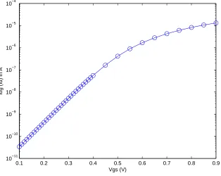
Figure 1.1:Idvs. Vgscharacteristics for IBM 65 nm technology atVdd= 1 V.
The behavior ofIdwith increasingVgs is shown in Figure 1.1. Idbehaves exponentially
in weak inversion region and holds a linear relationship in strong inversion region. Idvs
Vgs graph is used to extrapolate the threshold voltage of the MOSFET by looking at the
point where the graph deviates from its original exponential trajectory [2].
(b)Idvs. Vds
Behavior ofIdwith increasingVds in subthreshold and superthreshold regions are shown
in Figure 1.2 (a) and 1.2 (b), respectively. As observed from the Figure 1.2, Id holds
behaves linearly for higher values of Vds. It can be observed that the current flattens by
further increasing theVdsvalues and the current becomes roughly independent ofVdswhich
is called the saturation region.
0 0.2 0.4 0.6 0.8 1 0 0.5 1 1.5 2 2.5 3 3.5 4 4.5x 10
−9
Vds (V)
Id (A)
0 0.2 0.4 0.6 0.8 1 0 0.2 0.4 0.6 0.8 1 1.2 1.4 1.6 1.8x 10
−5
Vds (V)
Id (A)
Vgs = 0.7 V Vgs = 0.8 V
Vgs = 0.9 V
Vgs = 0.3 V
Vgs = 0.2 V
Figure 1.2: Id vs. Vds characteristics for IBM 65 nm technology (a) Subthreshold (b) Superthreshold.
(c) Dependence ofIdon Temperature andVth
Id is effected by Vth and temperature variations. Id increases exponentially with
de-creasing Vth, shown in Equation (1.2). Hence the circuit performance is higher with low
Vthtransistors. Temperature has an impact on parameters such as carrier mobility,
thresh-old voltage and junction leakage which vary theON current in a MOS transistor. Carrier
mobility decreases with an increase in temperature. An approximate relation of carrier
mobility with temperature is shown in Equation (1.6) [23].
µ(T) = µ(Tr)
µ T Tr
¶−kµ
(1.6)
where,T is the absolute temperature,Tris the room temperature, andkµis a fitting
param-eter generally in the range of 1.2-2.0. Vthreduces linearly with increase in temperature and
Vth(T) =Vth(Tr)−kvth(T −Tr) (1.7)
where,kvthis a constant and is in range of 0.5 to 3.0 mV/K. Junction leakage also increases
as the temperature is increased [23]. The overall effect of temperature on Id is different
for subthreshold and superthreshold operation. For subthreshold operation Id increases
with increasing temperature, and for superthreshold operation Id decreases with increase
in temperature [23]. Therefore, the circuit performance is best at high temperatures in
subthreshold, and worst at high temperatures for superthreshold operation. To improve
circuit performance of superthreshold circuits generally additional cooling mechanisms
such as heat sinks, water cooling, and liquid nitrogen are used which are not required for
subthreshold circuits.
To understand the behavior of circuits in subthreshold and superthreshold an inverter
is simulated using IBM 65 nm technology. Frequency and power characteristics of an
inverter operating in both subthreshold and superthreshold regions are shown in Figure
1.3 and 1.4, respectively. Power and frequency vary exponentially in subthreshold region.
Power consumption of an inverter operating at 0.3 V was 3.3 pW compared to 46.3 pW
at 1.0 V supply. The power consumption in subthreshold region is an order of magnitude
less when compared to strong inversion inversion. The reason for this is lowerVddvalue in
case of subthreshold operation. The delay of an inverter operating at 0.3 V was 29.56 ns
compared to 57.2 ps. The delay in subthreshold region is three orders of magnitude greater
compared to strong inversion operation. The reason for this is due to lowerON current in
0.1 0.2 0.3 0.4 0.5 0.6 0.7 0.8 0.9 1 105
106 107 108 109 1010 1011
Vdd (V)
log (Frequency) in Hz
Figure 1.3: Inverter frequency characteristics for IBM 65 nm technology and Vdd = 0.1 V to 0.9 V.
0.1 0.2 0.3 0.4 0.5 0.6 0.7 0.8 0.9 1
10−13 10−12 10−11 10−10
Vdd (V)
1.3 Summary
The operation of a MOS transistor in subthreshold has been discussed. Equations for drain
current and total energy in subthreshold have been presented in this chapter. The
exponen-tial dependence ofIdonVddandVgs in subthreshold region has been shown. The variation
in Id with varying temperature is discussed. Frequency and power characteristics of an
2. Motivation and Supporting Work
This chapter presents the related work supporting this research and provides the research
objectives. The research work related to subthreshold design is presented in Section 2.1.
The motivation for the proposed research is explained in Section 2.2. The formulated
thesis objectives are presented in Section 2.3. The summary of the key points discussed is
presented in the last section.
2.1 Supporting Work
Digital subthreshold design is gaining importance, especially for applications where
leakage power dissipation is the primary design metric and speed is not a criterion.
Leak-age power dissipation in CMOS circuits is increasing exponentially as the technology is
being scaled down [23]. Subthreshold design which utilizes the leakage current to
per-form useful computations is evolving as an ideal low power solution [2]. Subthreshold
designs suffer from a drawback of low operating speeds when compared to superthreshold
designs [9]. Research related to reducing the performance gap between subthreshold and
superthreshold circuits is gaining momentum.
The operation of digital circuits in the subthreshold region was considered as early as
1970, in which theoretical limits on supply voltage scaling were derived for a CMOS
inverter [19]. This limit is important to determine the minimum operating frequency of
CMOS circuits. The minimum energy operation of a CMOS circuit occurs in the
sub-threshold region [1]. This suggests that subsub-threshold operation can serve as a low energy
en-were derived [1][3][4]. The minimum energy point calculation is essential in designing
subthreshold circuits.
As the channel length reduces, several short channel effects (SCE) such as drain-induced
barrier lowering (DIBL) and electron/hole tunneling become important in CMOS circuits
[20]. These short channel effects have been examined in depth for subthreshold CMOS
operation, and an analytical model for channel current as a function of feature size has been
derived [20][21]. The effect of DIBL in subthreshold is lower compared to superthreshold
operation because of low drain voltages. Therefore, the need for high channel doping can
be eliminated in case of subthreshold circuits, which is otherwise required to overcome the
SCE in superthreshold circuits.
Subthreshold circuits are more sensitive to process, supply voltage and temperature
vari-ations compared to superthreshold circuits [8]. This higher sensitivity may cause
sub-threshold circuits to fail to function properly. To reduce the sensitivity to process, supply
voltage and temperature variations, newer logic families such as dualVT logic [8], variable
threshold voltage CMOS (VTCMOS) [18], and dynamic threshold voltage MOS (DTMOS)
[16] were proposed. Since DTMOS logic involves biasing the substrate with the input gate
signal, it can only be implemented in triple well technology. The increase in the process
complexity of DTMOS logic is compensated by its higher operating frequency.
The application spectrum of subthreshold circuits could be expanded by improving their
performance. Traditional logic families such as pseudo NMOS [15] and domino style [17]
have been implemented in subthreshold to achieve higher speeds. Pseudo NMOS offers
high operating speed in subthreshold region but is less desirable as it dissipates excess
static power when integrated in large scale. Dynamic circuits provide high speed operation
for subthreshold circuits but are less desirable due to additional overhead of charge keeper
transistors, which are needed to hold the value at dynamic output nodes. Dynamic output
desirable for subthreshold operation.
A logic family based on body biasing has been realized in [16] to improve the
subthresh-old operating frequency. Several models based on body biasing have been suggested in
[11][16]. Models suggested in [11][16] have either the gate or drain of the transistors tied
to the substrate. The substrate voltage increases with the input gate voltage reducing the
Vth, thereby increasing the speed. The advantage of using substrate biasing in subthreshold
circuits compared to superthreshold circuits is that it does not require additional limiter
transistors due to low operating voltages. Limiter transistors are required in superthreshold
circuits to limit the body potential to be less than 0.7 V to prevent CMOS latchup.
A circuit design approach to enhance the performance of subthreshold circuits was
sug-gested in [9]. In [9], asynchronous micro-pipelining of levelized network of PLAs was
used. A method to increase the speed of subthreshold interconnects has been suggested
in [10][14]. In [10][14], the voltage of the global interconnects was boosted through
addi-tional boosting circuitry. Subthreshold circuit performance could be improved by providing
higher gate voltage, while maintaining the supply voltage at a constant level. This approach
of boosting the gate voltage of transistors to improve the circuit performance has not yet
been considered.
Boosting the gate voltage of each and every transistor in a circuit is not required to
enhance the performance of subthreshold circuits. Transistors along the critical path
deter-mine the speed of the circuit. Boosting the gate voltage of the transistors along the critical
path can change the critical path itself. Hence, an optimal solution for the placement of
boosting circuitry is required. An optimization solution for leakage power minimization
is discussed in [12]. In [12], the optimization problem is formulated as an integer linear
program (ILP). Delay optimization of CMOS circuits by transistor reordering is suggested
The analysis suggests that the performance of subthreshold circuits can be improved
either by substrate biasing or by charge boosting. Substrate biasing is biasing the body of
the MOS transistor. The Vth of the transistors can be lowered through substrate biasing,
which increases theON current and thus improves the frequency of subthreshold circuits.
Charge boosting is boosting the Vgs of the transistors which leads to higher ON current.
The methods to improve the frequency of subthreshold circuits based on substrate biasing
and charge boosting are proposed in this research.
2.2 Motivation
The minimum energy operation of CMOS circuits occurs in subthreshold region of
op-eration. Therefore, subthreshold CMOS circuits can serve as an ideal low-energy solution.
However, subthreshold circuits suffer from a drawback of low operating speed. The
ap-plication spectrum of subthreshold circuits can be expanded by enhancing their frequency.
The frequency can be enhanced either by substrate biasing or charge boosting. The
ex-ponential dependence of Vth on ON current in subthreshold makes substrate biasing an
effective method to improve the frequency of subthreshold circuits. Charge boosting
en-hances the performance by increasing the Vgs of the transistors, which does not cause a
large overhead in the energy consumption making it effective for subthreshold operation.
The motivation for this research has led to the goal of enhancing the performance of
sub-threshold circuits. The objectives of this thesis are discussed in the next section.
2.3 Thesis Objectives
The goal of this thesis is to design methods which enhance the performance of subthreshold
circuits. To achieve this goal the following objectives are formulated.
• Design of standard cell libraries by implementing performance enhancement meth-ods and characterization of the delay and energy variations with Vdd for standard
cells.
• Placement of standard cells for optimal delay and power through integer linear pro-gramming (ILP) and implementation of standard cell library on the benchmark
cir-cuits.
2.4 Summary
The subthreshold circuit performance can be improved by increasing the ON current
flowing through the MOS transistors. TheON current can be increased either by substrate
biasing or charge boosting. Substrate biasing lowers theVthof the transistors, thereby
in-creasing theON current. Charge boosting enhances the frequency of subthreshold circuits
3. Performance Enhancement of
Sub-threshold Circuits
This chapter proposes two performance enhancement methods and presents analysis on
each method proposed. An overview of performance enhancement is discussed in Section
3.1. Section 3.2 presents two existing biasing techniques. A new approach to substrate
bi-asing is also discussed. A new performance enhancement technique using charge boosting
buffers is presented in Section 3.3. The key points discussed are summarized in Section
3.4.
3.1 Overview
The performance of a subthreshold circuit, is dependent on the ON current flowing
through the channel of MOS transistors. TheON current of a MOS transistor is dependent
on theVthand theVgs. Performance of subthreshold circuits can be improved by reducing
theVthand by increasing theVgs. The two existing biasing methods and a new approach to
substrate biasing involve reducing theVth of the CMOS devices. A new performance
en-hancement technique proposed increases theVgsof the transistors by using charge boosting
buffers.
3.2 Substrate Biasing
Substrate biasing is providing a bias voltage to the body of a MOS transistor. By
pro-viding a positive voltage to the body of an NMOS transistor relative to the source,Vth can
charging and discharging of the load capacitances, reducing the delay of the circuit and
thus improving the performance of subthreshold circuits. The threshold voltage of a four
terminal MOS transistor (Vth) is given by Equation (3.1) [22].
Vth=Vth0+γ( p
φ0+Vsb−
p
φ0) (3.1)
where,Vth0 is the threshold voltage with zero bias,γ is the body effect parameter,φ0is the
surface potential of MOS transistor and the source to body substrate bias (Vsb). As seen
from Equation (3.1), threshold voltage can be varied by varyingVsb. Vthreduces whenVsb
assumes negative values. Vsb becomes negative when the substrate of the device is forward
biased. Thus, the Vth of the device can be reduced by forward biasing the substrate of a
MOS transistor.
0 0.05 0.1 0.15 0.2 0.25 0.3 0.35 0
0.05 0.1 0.15 0.2 0.25 0.3 0.35
Vin (V)
Vout (V)
OH
OL IL V = 0.19IH V = 0.294
V = 0.12 V = 0.02193
Figure 3.2: Graphical representation of SNM for Gate-Gate biased inverter.
0 0.05 0.1 0.15 0.2 0.25 0.3 0.35 0
0.05 0.1 0.15 0.2 0.25 0.3 0.35
Vin (V)
Vout (V)
OH
OL
IH IL
V = 0.2 V = 0.2808
V = 0.0448 V = 0.1
0 0.05 0.1 0.15 0.2 0.25 0.3 0.35 0
0.05 0.1 0.15 0.2 0.25 0.3 0.35
Vin (V)
Vout (V)
OH
OL
IH IL
V = 0.1
V = 0.21 V = 0.0449
V = 0.2738
Figure 3.4: Graphical representation of SNM for Supply-Ground biased inverter.
Based on substrate biasing a method to improve the subthreshold circuit performance has
been designed. The two existing biasing methods and a new approach to substrate biasing
were applied to a CMOS inverter, and are shown in Figure 3.1 (a),(b) and (c), respectively.
The corresponding static noise margins for the three biased inverters are shown in 3.2, 3.3
and 3.4, respectively. The noise margin high is calculated asVOH -VIH and noise margin
low as VIL - VOL. The noise margin high and noise margin low for the circuit shown in
Figure 3.1(a) are 0.104 and 0.098, for circuit in Figure 3.1(b) are 0.808 and 0.055 and for
circuit shown in Figure 3.1(c) are 0.064 and 0.055 respectively. The biasing mechanism
shown in Figure 3.1(a) is termed Gate-Gate biasing [16], in which the substrates of PMOS
and NMOS are biased using a connection between respective gates and substrates. The
biasing mechanism shown in Figure 3.1(b) [11] is termed Drain-Drain biasing using a
connection between the respective drains and substrates. The proposed biasing mechanism
shown in Figure 3.1(c) is termed Supply-Ground biasing, in which the substrate of NMOS
0.1 0.15 0.2 0.25 0.3 0.35 0.4 0.45 105
106 107 108 109 1010
Vdd (V)
log (Frequency) in Hz
Gate−Gate Drain−Drain Supply−Ground
Figure 3.5: Frequency vs. Vddof an inverter for IBM 65 nm technology and various biasing schemes (a) Gate-Gate biasing (b) Drain-Drain biasing (c) Supply-Ground biasing.
The circuits shown in Figure 3.1 were simulated in subthreshold for IBM 65nm
technol-ogy and the corresponding power and delay characteristics with varying supply voltage are
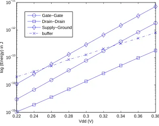
plotted, Figure 3.5 and 3.6. Frequency and power increase exponentially with supply
volt-age as observed from Figure 3.5 and 3.6 . It can also be observed that frequency and power
values are higher for the proposed Supply-Ground biasing compared to existing methods
(Gate-Gate and Drain-Drain biasing). This is because both NMOS and PMOS are biased
at all times in Supply-Ground biasing which is not the case with Gate-Gate biasing and
Drain-Drain biasing. In Gate-Gate biasing either NMOS or PMOS is biased depending
on input logic level of ’1’ and ’0’, respectively. In Drain-Drain biasing either NMOS or
PMOS is biased depending on output logic level of ’1’ and ’0’, respectively. Further, it can
be observed from Figure 3.5 and 3.6 that frequency and power values are higher in case of
Gate-Gate biasing compared to Drain-Drain biasing. The reason for this behavior is due
0.1 0.15 0.2 0.25 0.3 0.35 0.4 0.45 10−13
10−12 10−11 10−10 10−9 10−8 10−7
Vdd (V)
log (Power) in W
Gate−Gate Drain−Drain Supply−Ground
Figure 3.6: Power vs. Vdd of an inverter for IBM 65 nm technology and various biasing schemes (a) Gate-Gate biasing (b) Drain-Drain biasing (c) Supply-Ground biasing.
the input voltage is a step signal, the transistors are biased instantaneously when the input
signal is applied. In case of Drain-Drain biasing, the output voltage gradually changes and
would take the time equal to the delay of the circuit, to make a transition from one logic
level to another. Thus the substrate bias applied changes gradually from 0 to Vsbtd in 0 to
tdseconds (wheretdis the delay of the gate andVsbtd is the substrate bias voltage after the
time td). The substrate bias voltage for Drain-Drain biasing as a function of time can be
modelled as shown in Equation (3.2).
Vsb(t) =Vsbtd
µ t td
(3.2)
where, Vsbtd is the substrate bias voltage at timet =td. Substituting the value ofVsb(t)in
Equation (3.1) results in variation of threshold voltage for Drain-Drain biasing as a function
Vth(t) = Vth0+γ( s
φ0+Vsbtd
µ t td
−pφ0) (3.3)
The expression forONcurrent in subthreshold as given in Equation (2.2) can be simplified
as shown below in Equation (3.4).
ION =A1exp(A2−A3Vth) (3.4)
where,
A1 =
W Lef f
µef fCox(m−1)VT2(1−exp
−Vds
VT )
A2 =
Vgs
mVT
A3 =
1
mVT
Substituting the expression forVth(t)from Equation (3.3) into Equation (3.4) gives the
expression forION as a function of time as shown in Equation (3.5).
ION =A1exp(A2−A3(Vth0+γ( s
φ0+Vsbtd
µ t td
−pφ0))) (3.5)
Equation (3.5) can be simplified as shown in Equation (3.6).
ION =A1exp Ã
A2−A4−γA3 s
φ0+Vsbtd
µ t T ¶! (3.6) where,
A4 =A3Vth0−γA3 p
φ0
The averageON current can be obtained by integrating Equation (3.6) with limits on
Iavg = 1
td
Z td
0
IONdt (3.7)
Iavg =
2A1exp(A2 −A4)
Vsbtdγ2A23 ³
(γA3 q
φ0+Vsbtd + 1) exp(−γA3 q
φ0+Vsbtd)
−(γA3 p
φ0+ 1) exp(−γA3 p
φ0) ´
(3.8)
The expression forON current in Gate-Gate biasing is shown in Equation (3.9)
IGate−Gate =A1exp ³
A2 −A4−γA3 q
φ0+Vsbtd
´
(3.9)
Iavg can be written as shown below
Iavg = I1−I2 (3.10)
where,
I1 = IGate−Gate
2¡γA3 p
φ0+Vsbtd + 1
¢
Vsbtdγ2A23
(3.11)
I2 = IGate−Gate
2¡γA3 p
φ0+Vsbtd + 1
¢
exp(−γA3
√
φ0)
Vsbtdγ2A23exp(−γA3 p
φ0 +Vsbtd)
(3.12)
To calculate the values ofI1 andI2 we needγ,φ0, Vsbtd andA3. The value ofA3 can
be calculated as shown below.
A3 =
1
mVT
= 1
60∗10−3∗26∗10−3 = 641.025
Substituting the approximate values for γ as 0.504 [22] andφ0 as 0.975 [22], VsbT = -Vdd
I2we get
I1 = 0.0375IGate−Gate
I2 ≈ 0
Iavg = I1−I2 = 0.0375IGate−Gate (3.13)
It can be observed that theON current in case of Gate-Gate biasing is 26 times that of
theON current in case of Drain-Drain biasing. This difference in theON current affects
the delay and power of the standard cells. The delay and power values for AND02 with
Gate-Gate and Drain-Drain biasing are shown in Table 3.1. It can be observed that the
delay in case of Gate-Gate biasing is 75.28 ns which is considerably less when compared
with 125.9 ns in case of Drain-Drain biasing. The power consumption in case of Gate-Gate
biasing is 1.467 nW which is four times higher when compared with 0.337 nW in case of
Drain-Drain biasing.
Table 3.1: Delay and power values for AND02 withVdd= 0.3 V.
Biasing Delay Power
Gate-Gate 75.28 ns 1.467 nW
Drain-Drain 125.9 ns 0.337 nW
In CMOS circuits typically the substrate of NMOS is tied to ground and substrate of
PMOS is tied to Vdd. This is done to avoid the possibility of CMOS latch up. CMOS
latch up occurs when the body potential is typically greater than 0.7 V. Substrate biasing in
superthreshold circuits can cause CMOS latch up. However, due to low operating voltages
in case of subthreshold operation substrate biasing would not cause any latchup. Further, in
case of Drain-Drain biasing the output noise can cause some variation in delay and power
values when compared to Gate-Gate and Supply-Ground biasing, and would have no effect
3.3 Charge Boosting
A new performance enhancement technique, namely charge boosting, improves the
sub-threshold circuit performance by increasing theVgsof the transistors using charge boosting
buffers. The boostedVgs provided to the transistors would increase the ON current. The
ON current of a transistor is exponentially dependent onVgsin subthreshold region, as seen
in Figure 1.1. Therefore, a slight increase in Vgs would cause an exponential increase in
ON current, which causes the load capacitors to charge and discharge in short time. Hence
the delay of the circuit is reduced and the performance is enhanced.
The Vgs of the transistors can be increased by the use of charge boosting buffers. The
charge boosting buffer circuit which is designed to increase the Vgs is shown in Figure
3.7. The charge boosting buffer circuit is designed to amplify a step signal from 0 V to
0.3 V into a step signal from -0.1 V to 0.5 V, with -0.1 V as the voltage of sink and 0.5
V as the supply voltage of the buffer circuit. These buffers can be integrated into normal
standard cells to form a standard cell library with higher operating frequency. An inverter
integrated with a buffer is shown in Figure 3.8. The simulation of the buffer circuit with
output characteristics is shown in Figure 3.9.
Figure 3.8: Charge boosting buffer providing higherVgsto an inverter withVdd= 0.3 V.
Figure 3.9: Transient input-output characteristics of charge boosting buffer simulated in
3.4 Summary
Two existing biasing methods and a new approach to substrate biasing have been
pre-sented, namely Gate-Gate biasing, Drain-Drain biasing and Supply-Ground biasing
respec-tively. A new performance enhancement technique using charge boosting buffers has been
proposed. An analytical expression comparing the ON current for the case of Gate-Gate
and Drain-Drain biasing has been derived. The equation derived indicates thatON current
in case of Gate-Gate biasing is 26 times that of the ON current in case of Drain-Drain
biasing. This higher ON current leads to lower delay and higher energy consumption in
case of Gate-Gate biasing when compared to Drain-Drain biasing. Each performance
en-hancement method comes with a cost of higher energy consumption. Hence, it is essential
to optimize the placement of the performance enhanced standard cells so as to achieve the
best performance with minimal additional overhead of energy consumption. An
4. Cell Placement Optimization for
Min-imizing Energy Consumption
This chapter presents an algorithm and a methodology to optimize the placement of
stan-dard cells for optimal delay and energy. An overview of optimization is discussed in
Sec-tion 4.1. An algorithm useful to find an optimal soluSec-tion for placement of cells in CMOS
circuits is presented in Section 4.2. An optimization flow for implementing the
optimiza-tion algorithm is presented in Secoptimiza-tion 4.3. The key points discussed are summarized in the
summary section.
4.1 Overview
As discussed in Chapter 3, each design methodology improves the performance of the
subthreshold circuit by increasing theONcurrent flowing through the transistor. However,
due to an increase in the ON current the power consumption increases. Hence, it is
es-sential to optimize the placement of the high performance cells so as to achieve the best
performance with minimal additional cost of power consumption. The performance of a
large circuit is determined by the path with the longest delay, the critical path. Placing the
high performance cells along the critical path would change the original critical path in the
modified circuit. Hence an algorithm and methodology is required for the placement of the
cells to achieve the best performance with constraints of having the least additional power
consumption, and the original critical path remaining unchanged. The methodology and
4.2 Optimization Algorithm
CMOS circuits can be represented in the form of a network. Network models can be
used as an aid in solving several optimization problems. The algorithm that is used to solve
the optimization problem is called Critical Path Method (CPM) [24]. CPM can be used to
determine the critical path of the circuit, and also to determine how long each activity can
be delayed without affecting the total performance of the circuit. An activity is defined as
the transition of inputs into outputs for any given standard cell in the circuit. A complete list
of all the activities that comprise the operation of the circuit is required to apply CPM. To
understand the algorithm with ease an exemplary network is considered, shown in Figure
4.1. To apply CPM the network has to be directed-acyclic graph. Acyclic graph indicates
absence of feed back loops in the circuit.
Figure 4.1: Network model of a CMOS circuit.
Each node in the network shown in Figure 4.1 represents a signal and each arc in the
network represents a standard cell. The time consumed for a signal to travel from one
node to the next adjacent node is given by the delay of standard cell that represents an arc
between the nodes. The arcs between start node and the input nodes are represented by
dummy cells with 0 seconds delay time. Similarly the arcs between the output nodes and
the end node are represented by dummy cells as shown in Figure 4.1. Each node in the
A are as shown in Figure 4.2. Successors for any node X are defined as the neighboring
nodes that are dependent on node X for their production. The successors for node A are as
shown in Figure 4.3.
Figure 4.2: Predecessors of node A.
Figure 4.3: Successors of node A.
A list of all the nodes, their successors and predecessors, along with duration of all
activities or arcs, is required to apply CPM. A table representing the list of nodes, their
successors and predecessors is shown in Table 4.1 and the list of all arcs and their duration
is shown in Table 4.2.
The two key building blocks in CPM are the concepts of early event time (ET) and late
event time (LT) for a node. The early event time for a node i, represented by ET(i), is
defined as the earliest time at which the nodeican be produced. The late event for a node
i, represented by LT(i), is the defined as the latest time at which the nodeican be produced.
Table 4.1: List of all nodes, their successors and predecessors.
Node Successors Predecessors
Start IN1, IN2, IN3
-IN1 A Start
IN2 A, B Start
IN3 B Start
A OUT1, OUT2 IN1, IN2
B OUT2 IN2, IN3
OUT1 END A
OUT2 END A, B
END - OUT1, OUT2
Table 4.2: List of all arcs, corresponding standard cells and their delays.
Arc Standard cell Delay
Start→IN1 Dummy 0 ns
Start→IN2 Dummy 0 ns
Start→IN3 Dummy 0 ns
IN1→A AND02 177.1 ns
IN2→A AND02 177.1 ns
IN2→B XOR02 83.47 ns
IN3→B XOR02 83.47 ns
A→OUT1 INV02 29.56 ns
A→OUT2 OR02 208.2 ns
B→OUT2 OR02 208.2 ns
OUT1→END Dummy 0 ns
OUT2→END Dummy 0 ns
required to produce the signal at that node. The early event time for the output nodes will
be equal to the delay of the circuit.
4.2.1 Computation of Early Event Time
The computation of early event time for each node begins with the start node. Represent
the start node as node 1 and assign numbers to each node. Early event time for node 1
is assumed to be 0, ET(1) = 0. Then compute ET(2), ET(3), etc. and stop when ET(end
are required. Thus, computation of ET is in a particular order from start node to end node.
Referring to the network shown in Figure 4.1, and Figure 4.2 the predecessors of node A,
the early event time of node A is calculated as shown below [24].
ET(A) =max
ET(IN1) + delay of AND gate
ET(IN2) + delay of AND gate
From the above example it is clear that computation of ET(i) requires the knowledge of
ET(1), ET(2), ..., ET(i-1). Computation of early event time for any general nodeican be
summarized as follows:
STEP 1: Find all the predecessors of nodei.
STEP 2: To the ET for each predecessor of node i add the delay of the gate or arc
connecting the predecessor to nodei.
STEP 3: ET(i) equals the maximum of the sums computed in Step 2.
4.2.2 Computation of Late Event Time
The computation of late event time for each node begins with the end node. To compute
the latest event time for each node, work backwards in descending order until LT(1) is
reached. Assume that LT(end) is equal to ET(end). Referring to the network shown in
Figure 4.1, and Figure 4.3 the successors of node A, the latest event time of node A is
calculated as shown below [24].
LT(A) =min
LT(OUT1)− delay of INVERTER
LT(OUT2)− delay of OR gate
Computation of latest event time for any general nodeican be summarized as follows:
STEP 1: Find all the successors of nodei
STEP 2: To the LT for each successor of nodei subtract the delay of the gate or arc
STEP 3: LT(i) is the smallest of the differences determined in step 2.
The early event time and latest event time computed for all the nodes in the network are
shown in Table 4.3
Table 4.3: Early event time and latest event time for all nodes.
Node Early event time Latest event time
Start 0 ns 0 ns
IN1 0 ns 0 ns
IN2 0 ns 0 ns
IN3 0 ns 93.63 ns
A 177.1 ns 177.1 ns
B 83.47 ns 177.1 ns
OUT1 206.66 ns 385.3 ns
OUT2 385.3 ns 385.3 ns
END 385.3 ns 385.3 ns
4.2.3 Total Float
For any arc joining the nodes i and j, the total float, represented by TF(i,j), of the
standard cell or arc (i,j) is the amount of time by which the delay of the standard cell can
be extended without affecting the circuit performance and also without affecting the critical
path. The total float of the standard cells across the critical path is 0. The total float for any
arc (i,j) can computed as shown in Equation (4.1).
T F(i, j) =LT(j)−ET(i)−tij (4.1)
wheretij is the delay of the standard cell represented by the arc (i,j).
The value of total float computed for all the arcs is shown in Table 4.4.
Since the arcs with total float equal to 0 fall on the critical path, by joining all such arcs
the critical path can be formed. The critical paths formed by joining such arcs from Table
4.4 are Start → IN1→ A →OUT2 → END and Start→ IN2 →A → OUT2→ END.
Table 4.4: List of all arcs and their respective total float.
Arc Total float
Start→IN1 0 ns
Start→IN2 0 ns
Start→IN3 93.63 ns
IN1→A 0 ns
IN2→A 0 ns
IN2→B 93.63 ns
IN3→B 93.63 ns
A→OUT1 178.64 ns
A→OUT2 0 ns
B→OUT2 93.63 ns
OUT1→END 178.64 ns
OUT2→END 0 ns
can be delayed by 93.63 ns without affecting the overall performance and the critical path.
Similarly the arc A→OUT1 represented by INV02 can be delayed by 178.64 ns. Hence by replacing the XOR02 and INV02 with modified cells of the same functionality which
have lower power consumption and higher delay depending on the total float will not affect
the performance of circuit.
4.3 Optimization Flow for Implementing CPM
As discussed in Section 4.1, the purpose of optimization is to find an optimal solution for
placement of high performance cells in the circuit with constraints of having the least
addi-tional power consumption, and the original critical path remaining unchanged. To achieve
this, first replace all the standard cells in the circuit with high performance cells. Apply
the CPM algorithm to determine total float of each cell present in the circuit. If the total
float of any particular high performance cell is greater than the difference of the delay of a
standard cell and its corresponding high performance cell, then replace that particular high
performance cell with a normal cell. Thus, by replacing all possible high performance cells
A flow chart representing the methodology is shown in Figure 4.4.
4.4 Summary
A CPM algorithm has been discussed which is used to find the critical path of the circuit.
CPM is also used to determine how long the delay of each cell can be extended without
affecting the circuit performance and critical path. An optimization flow for implementing
the CPM algorithm to determine the placement of the performance-enhanced standard cells
has been presented. Placement of these high-performance cells is such that total power
con-sumption is minimized while the critical path remains unchanged and the best performance
enhanced normal cell − delay is required
No modification NO YES
cell, if total float > (delay of
cell)
with a corresponding regular cell
Replace the perform− For each
enhanced cells
Replace all the standard cells
enhanced cell in the netlist Apply CPM and compute total
circuit
netlist of a benchmark
placement with optimal cell benchmark circuit Transistor level SPICE
in the netlist with performance−
float for each performance−
of performance−
ance−enhanced cell
SPICE netlist of a
5. Results and Analysis
This chapter presents the results, analysis, delay and energy characteristics obtained from
the simulations on each standard cell. The simulation setup is explained in Section 5.1. The
results obtained from the simulations for each standard cell are presented in Section 5.2.
The delay and energy variations are characterized and the analysis is presented for each
standard cell library in Section 5.2. The summary of the performance-enhanced standard
cell library is presented in Section 5.2. The implementation of the performance-enhanced
cell library designed on the benchmark circuits and the effectiveness of the optimization
algorithm are presented in Section 5.3.
5.1 Simulation Setup
An IBM 65 nm technology file is used to perform all the simulation for this thesis. The
transient analysis for the standard cells is performed using HSPICE. PERL scripts are used
to automate the simulation runs for standard cells withVddranging from 0.2 V to 0.4 V. To
account for the process variations the simulations are performed for performance corners
(FF, SS), transistor mismatch corners (FS, SF) and the nominal corner (TT). The
simu-lations are performed for worst case temperature of 125◦ C, best case temperature of 0◦
C, and nominal temperate of 25◦ C to account for the temperature variations. The
de-signed standard cell library is implemented on the ISCAS 85 benchmark circuits and these
benchmark circuits are chosen because they form a network of directed acyclic graphs [6].
A general setup used for the simulations on substrate-biased and charge-boosted standard
Vout
Vsb
0.3 V
Standard Cell
Biasing Substrate
in V
Figure 5.1: Substrate biasing applied to a standard cell withVdd =0.3 V.
0.5 V
−0.1 V
V V
Buffer
Charge Boosting Standard
Cell
0.3 V
in out
Figure 5.2: Charge boosting buffer providing higherVgs to a standard cell withVdd=0.3 V.
5.2 Performance Enhanced Standard Cell Library
The delay and energy characteristics along with the analysis for each standard cell are
presented in this section. A performance-enhanced standard cell library is built by
example, Drain-Drain biasing when applied on a regular standard cell library results in
Drain-Drain standard cell library. The results obtained by implementing the four
perfor-mance enhancement methods on standard cells such as Inverter, AND, NAND, OR, NOR,
AND-OR gate, OR-AND gate, XOR and XNOR are discussed below.
5.2.1 Inverter
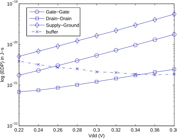
The regular inverter cell has a delay of 29.56 ns and an energy consumption of 0.08 fJ
at 0.3 V. Performance enhancement methods discussed earlier increase the ON current of
the transistors either by substrate biasing or charge boosting. This leads to faster charging
and discharging of load capacitances, reducing the delay. The higherON current leads to
higher energy consumption. Thus the delay of performance-enhanced inverter is lower and
energy consumption is higher compared to regular inverter cell.
The delay and energy values for a regular inverter cell and the performance enhanced
inverter operating at 0.3 V supply are shown in Table 5.1. The analysis for the difference
in behavior of delay and energy observed in the case of Gate-Gate biasing, Drain-Drain
biasing, Supply-Ground biasing and charge boosting is presented below.
Table 5.1: Delay and energy values of an inverter at 0.3 V for IBM 65 nm technology.
Methodology Delay (s) Energy (J)
Regular 2.956e-08 7.927e-17
Gate-Gate 1.314e-08 9.966e-15
Drain-Drain 1.394e-08 6.475e-15
Supply-Ground 8.740e-09 2.960e-14 Charge boosted 7.062e-09 1.320e-14
(a) Delay
The delay value is least in the case of charge boosting, followed by Supply-Ground biasing,
lower delay in the case of charge boosting compared to substrate biasing is the higherIon
in the case of charge boosting. Ionis exponentially related to Vgs -Vth. Hence an increase
in the Vgs and an equivalent decrease in the Vth change the Ion by the same value. The
increase inVgsin case of charge boosting for a 0.3 VVddis 0.2 V. The reduction inVthdue
to substrate biasing can be calculated from Equation (3.1) as shown in Equation (5.1).
∆Vth=γ(
p
φ0+Vsb−
p
φ0) = 0.504(
√
0.975−0.3−√0.975) = 0.083V (5.1)
Since∆Vgsis higher than∆Vth, theIonin case of charge boosting is higher than substrate
biasing, leading to higher performance. The delay in case of charge boosting is
approxi-mately 4 times smaller compared to the regular inverter due to the 0.2 V boost in Vgs as
observed from Table 5.1. The limit of the boosted voltage for a charge boosting buffer with
a 0.3 VVddis 0.29 V with a valid functionality. But with a boosted voltage of 0.29 V any
noise in the input signal will result in a functionality error of the charge boosting buffer.
Thus, to maintain at least 0.1 V as a noise margin for a 0.3 VVdd, the charge boosting buffer
was designed to have a boosted voltage of 0.2 V. The boosted voltage can be expressed as
0.66∗Vdd. The boosted voltage decreases with scaling down of the technology node. Since theVthdecreases with technology scaling, the operatingVddfor the subthreshold operation
would decrease, resulting in lower boosted voltage..
The delay in case of Supply-Ground biasing is lowest among the three biasing methods.
This is because in case of Supply-Ground biasing the substrates of PMOS and NMOS are
biased at all times and do not change dynamically which is the case with the other two.
In case of Gate-Gate biasing and Drain-Drain biasing the substrate of PMOS and NMOS
are biased with respective input and output transitions. Gate-Gate biasing has lower delay
compared to Drain-Drain biasing because of approximately 26 times higherIon as shown
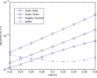
in Equation (3.13). The delay variation for the four performance enhancement methods in
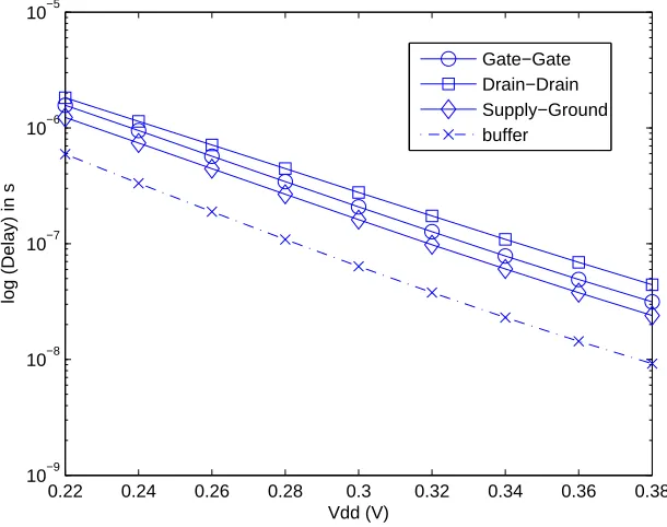
case of an inverter with varyingVddis shown in Figure 5.3. The delay of all the performance
delay reduces. Further, the reduction in delay with increasingVdd is exponential in nature
because of the exponential dependence ofIononVgs andVthas observed from Figure 5.3.
0.22 0.24 0.26 0.28 0.3 0.32 0.34 0.36 0.38 10−9
10−8 10−7 10−6
Vdd (V)
log10 (Delay) s
Gate−Gate
Drain−Drain
Supply−Ground
buffer
Figure 5.3: Inverter delay characteristics with varyingVddin IBM 65 nm technology.
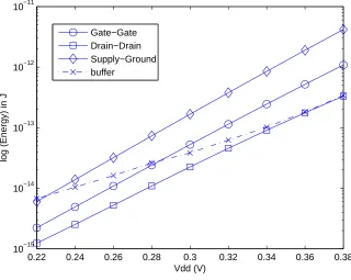
(b) Energy
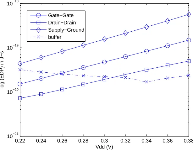
The energy due to leakage is the main component of energy consumption in
subthresh-old. The dependence of leakage energy onVth,Vddandtdfrom Equation (1.5) is shown in
Equation (5.2).
EL∝(e−Vth)Vddtd (5.2)
TheVth reduces with substrate biasing and the energy increases exponentially with the
re-duction in Vth. The ∆Vth is highest for Supply-Ground biasing, followed by Gate-Gate
biasing and Drain-Drain biasing as discussed earlier, due to which the energy consumption
is lowest in case of Drain-Drain biasing followed by Gate-Gate biasing and Supply-Ground
in-0.22 0.24 0.26 0.28 0.3 0.32 0.34 0.36 0.38 10−16
10−15 10−14 10−13 10−12
Vdd (V)
log (Energy) in J
Gate−Gate Drain−Drain Supply−Ground buffer
Figure 5.4: Inverter energy characteristics with varyingVdd in IBM 65 nm technology.
creases exponentially with increasingVddin case of substrate biasing, shown in Figure 5.4.
AsVddincreases the substrate bias voltageVsbassumes more negative values. This leads to
a decrease in the value ofVth. AsVthreduces the energy consumption increases, shown in
Equation (5.2). The energy variation in case of charge boosting is different from substrate
biasing. In case of charge boosting theVthremains the same as regular inverter cell. Hence
the energy consumption is dependent onVddand the energy consumed by the buffer. As the
supply voltage increases the increase in energy consumption is not exponential which is the
case with substrate biasing, shown in Equation (5.2). Due to the linear dependence onVdd,
charge boosting consumes less energy compared to substrate biasing at higher values of
Vdd. The Drain-Drain biasing has the lowest energy among the four methods u