Design of Low Power High Performance 32-bit
RCA and CSA with Proposed Adder Cell
K. Venkata Ramanaiah
Head, Department of ECE, Y.S.R. Engineering College of Yogi Vemana University, Proddatur, Y.S.R (Dt.) A.P., India
ABSTRACT: In this work 32-bit RCA and CSA have been proposed based on one bit Full Adder with Ten transistors. The Two different circuits have been simulated by using Microwind3.1 VLSI CAD Tool. Simulation for the designed circuits were carried out with 4-bit, 16-bit and 32-bit ripple carry adders and Carry Skip adders. Various parameters such as delay, power dissipation, PDP have been determined from adder layout of feature size 90nm and 65nm technologies. The adder circuits have been analyzed using BSIM 4 parameter analyzer. Finally the simulation analysis were compared with conventional and proposed Adders in terms of total power consumption, delay, area and power delay product.
KEYWORDS:CMOS; Conventional Logic; Full Adder; Low Power design; 4-bit RCA/CSA; 16-bit RCA/CSA; 32-bit RCA/CSA; RCA: Ripple Carry Adder; CSA: Carry Skip Adder;
I.INTRODUCTION
Full adder circuit is functional building block and most critical component of complex arithmetic circuits like microprocessors, digital signal processors or any ALUs. Almost every complex computational circuit requires full adder circuitry. The entire computational block power consumption can be reduced by implementing low power techniques or by less transistor count. Scaling improves transistor density and functionality on a chip. Scaling helps to increase speed and frequency of operation and hence higher performance. As voltages scale downward with the geometries threshold voltages must also decrease to gain the performance advantages of the new technology but leakage current increases exponentially. Delay is reduced and efficiency is improved compared to Ref.[1]. Among all Adders carry select adder is the fastest adder hence it can be designed by using Proposed ripple carry adder.
Low-power design techniques minimize active leakage power in nano scale CMOS very large scale integration (VLSI) systems. Developers of battery powered devices often have the challenge to offer high levels of functionality and performance while simultaneously maximizing battery life. In some cases, developers are also challenged to develop next generation products with no battery at all, requiring energy harvesting from environmental sources such as heat, vibration and light. Furthermore, as the demand for longer battery life and smaller batteries increases in more applications, users continue to demand more functionality and higher performance in their products. To maximize functionality and battery life, developers of these battery-powered applications must consider many factors in their system architecture and design. In these applications, the microcontroller is a primary power consumer and developers must carefully consider the way energy is used.
In current CMOS technologies, the sub threshold leakage current is much larger than the other leakage current components. This current can be calculated by using the following equation.
IDS=K(1-℮VDS/VT)℮(VGS-VT +αVDS/αVT).
Where K and α are functions of the technology and α is the drain-induced barrier lowering coefficient. Even in current generation technology, sub threshold leakage power dissipation is comparable to the dynamic power dissipation, and the fraction of the leakage power will increase significantly in the near future.[2],[3].
II. CONVENTIONAL FULL ADDER
Fig .1 Logic Circuit of Conventional Full adder.
Fig .2 Transistor Level Circuit of Conventional Full adder.
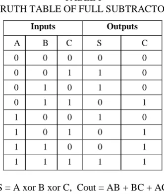
The two outputs S and Cout represent sum and carry, respectively. The logic circuit and transistor level schematic of full adder is shown in Fig.1 & Fig 2. and truth table in Table I.
TABLE I
TRUTH TABLE OF FULL SUBTRACTOR
Inputs Outputs
A B C S C
0 0 0 0 0
0 0 1 1 0
0 1 0 1 0
0 1 1 0 1
1 0 0 1 0
1 0 1 0 1
1 1 0 0 1
1 1 1 1 1
S = A xor B xor C, Cout = AB + BC + AC Where A, B, Cin inputs and S, Cout are outputs.
III. DESIGN OF 4-BIT, 16-BIT AND 32-BIT RCA AND CSA WITH CONVENTIONAL FULL ADDER
to be implemented in digital computers using basic gates like AND, OR and universal gates like NOR, NAND etc. Among all the arithmetic operations if we can implement addition then it is easy to perform multiplication (by repeated addition), subtraction (by negating one operand) or division (repeated subtraction).[5],[6].
Half Adders can be used to add two one bit binary numbers. It is also possible to create a logical circuit using multiple full adders to add N-bit binary numbers. Each full adder inputs a Cin, which is the Cout of the previous adder. This kind of adder is a Ripple Carry Adder, since each carry bit "ripples" to the next full adder.[7]. The block diagram of 4-bit Ripple Carry Adder is shown here below.
Fig .3. 4-Bit RCA with Conventional Full adder.
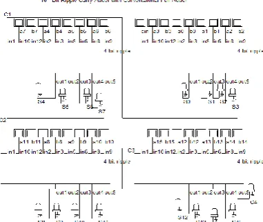
Fig .4. 16-Bit RCA with Conventional Full adder.
Fig .5. 32-Bit RCA with Conventional Full adder.
stages [10]. • If each Ai # Bi in a group, then we do not need to compute the new value of Ci+1 for that block; the carry-in of the block can be propagated directly to the next block. • If Ai = Bi = 1 for some i in the group, a carry is generated which may be propagated up to the output of that group. • If Ai = Bi = 0, a carry, will not be propagated by that bit location. The basic idea of a carry-skip adder is to detect if in each group all Ai # Bi and enable the block„s carry-in to skip the block when this happens as shown in figure1. In general a block-skip delay can be different from the delay due to the propagation of a carry to the next bit position [9],[11]. With carry skip adders, the linear growth of carry chain delay with the size of the input operands is improved by allowing carries to skip across blocks of bits, rather than rippling through them. Fig 6 represents 4-bit carry skip adder with conventional full adder.
Fig .6. 4-Bit CSA with Conventional Full adder.
Fig .7. 16-Bit CSA with Conventional Full adder.
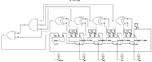
IV. DESIGN OF PROPOSED FULL ADDER CELL
The Circuit diagram of proposed Full Adder with ten transistors is shown in Fig 5. and the designed circuit is used for implementing four bit, sixteen bit and thirty two bit ripple carry and carry skip adders for analyzing the performance of proposed adder cell in terms of delay, power, area and power delay product.[1].
Table II, and III represents performance analysis of conventioanl and Proposed Ripple Carry Adders with 4, 16, and 32-bits at 90nm and 65nm technologies, Table IV, and V represents performance analysis of conventioanl and Proposed Carry Skip Adders with 4, 16, and 32-bits at 90nm and 65nm technologies, Table VI shows no. of transistots required for implementing Conventional and Proposed one bit Full Adder, Table VII shows no. of Full Adder cells required for implementing 4, 16, and bit RCA/CSA`s, where as Fig 3., Fig 4. and Fig 5. Shows 4-bit, 16-bit and 32-bit RCA`s by Conventional Full Adder, and Fig 6., Fig 7 and Fig 8. Shows 4-32-bit, 16-32-bit and 32-32-bit CSA`s by Conventional Full Adder, Fig 9. Represents Proposed Full Adder with ten transistors, Fig 10, Fig 11. and Fig 12. Shows 4-bit, 16-bit and 32-bit RCA`s by Proposed Full Adder, and Fig 13, Fig 14 and Fig 15. Shows 4-bit, 16-bit and 32-bit CSA`s by Proposed Full Adder.
Fig .9. Full adder cell with ten transistors.
Fig .10. 4-bit Rippple Carry Adder with proposed adder cell.
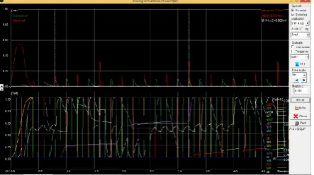
Fig.12. 32-bit Rippple Carry Adder cell proposed adder cell.
Fig .13. 4-bit CSA with proposed adder cell.
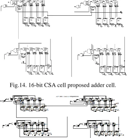
Fig.14. 16-bit CSA cell proposed adder cell.
V. SIMULATION RESULTS
Performance analysis of 4-bit, 16-bit and 32-bit RCA and CSA`s with Conventional and proposed Adder cell is analyzed in Microwind 3.1 CAD tool in 90nm and 65 nm technologies. Comparison is done in terms of power, delay, area and power delay product in 90nm and 65nm technologies at room temperature.[12].
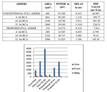
Fig. 16& Fig. 17. represents Waveform of 32-bit RCA & CSA with Proposed Adder Cell at 65nm (V vs I).
Fig. 16. Waveform of 32-bit RCA with Proposed Adder Cell at 65nm (V vs I).
Fig.17. Waveform of 32-bit CSA with Proposed Adder Cell at 65nm (V vs I).
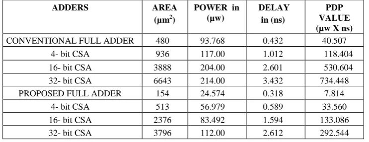
Fig. 18, Fig. 19, Fig. 20& Fig. 21 represents Graphical analysis of the results tabulated in Tables II, III, IV and V in terms of Area, Power, Delay and Power Delay.
TABLE II
SIMULATION RESULTS OF CONVENTIONAL AND PROPOSED CIRCUITS IN 90NM/27OC
ADDERS AREA
(µm2)
POWER in (µw)
DELAY in (ns)
PDP VALUE (µw X ns) CONVENTIONAL FULL ADDER 770 205.00 0.480 98.40
4- bit RCA 1380 252.00 2.295 578.34 16- bit RCA 3588 433.00 12.05 5217.6 32- bit RCA 6348 464.00 23.67 10982.8 PROPOSED FULL ADDER 252 48.849 0.345 16.852
Fig. 18. Graphical Analysis of the results tabulated in Table II.
TABLEIII
SIMULATIONRESULTS OFCONVENTIONALANDPROPOSEDCIRCUITSIN65NM/27OC
ADDERS AREA
(µm2)
POWER in (µw)
DELAY in (ns)
PDP VALUE (µw X ns) CONVENTIONAL FULL ADDER 480 93.768 0.432 40.507
4- bit RCA 864 98.185 1.118 109.77 16- bit RCA 2160 167.00 5.912 987.30 32- bit RCA 3888 195.00 11.610 2263.9 PROPOSED FULL ADDER 154 24.574 0.318 7.814
4- bit RCA 280 14.945 0.455 6.799 16- bit RCA 1224 30.737 2.486 76.41 32- bit RCA 2088 31.025 3.396 105.36
TABLEIV
SIMULATIONRESULTS OFCONVENTIONALANDPROPOSEDCIRCUITSIN90NM/27OC
ADDERS AREA
(µm2)
POWER in (µw)
DELAY in (ns)
PDP VALUE (µw X ns) CONVENTIONAL FULL ADDER 770 205.00 0.480 98.40
4- bit CSA 1564 304.00 2.085 633.84
16- bit CSA 6348 475.00 5.060 2403.5 32- bit CSA 10998 478.00 6.800 3250.4 PROPOSED FULL ADDER 252 48.849 0.345 16.852 4- bit CSA 814 151.00 1.205 181.955 16- bit CSA 3864 199.00 3.280 652.72 32- bit CSA 6392 260.00 5.380 1398.8
Fig. 20. Graphical Analysis of the results tabulated in Table IV.
TABLEV
SIMULATIONRESULTS OFCONVENTIONALANDPROPOSEDCIRCUITSIN65NM/27OC
ADDERS AREA
(µm2)
POWER in (µw)
DELAY in (ns)
PDP VALUE (µw X ns) CONVENTIONAL FULL ADDER 480 93.768 0.432 40.507
4- bit CSA 936 117.00 1.012 118.404 16- bit CSA 3888 204.00 2.601 530.604 32- bit CSA 6643 214.00 3.432 734.448 PROPOSED FULL ADDER 154 24.574 0.318 7.814
Fig.21. Graphical Analysis of the results tabulated in TableV.
TABLEVI
NO.OFTRANSISTORSREQUIREDFORIMPLEMENTINGADDERCELL
No. of Transistors Pmos Nmos
Conventional 14 14
Proposed 5 5
TABLEVII
NO.OFFULLADDERCELLS REQUIREDFORIMPLEMENTING4-16&32-BITRCA
RCA/CSA 1-bit Full Adder Cells
4- bit RCA/CSA 4 16- bit RCA/CSA 16 32- bit RCA/CSA 32
VI.CONCLUSION
In this work 32-bit RCA and 32-bit CSA have been proposed. The Proposed adder cells consists of 320 transistors for 32 bit RCA and 480 transistors for 32 bit CSA compare to conventional CMOS logic. The proposed circuit simulated using Microwind/DSCH 3.1 tool in 90nm and 65nm technologies with BSIM4 analyzer. Finally observed that 32-bit Ripple Carry Adder with Proposed Adder cell is Energy Efficient one as the power delay product value is less compared to other 32-bit architectures. By using proposed adder cell32-bit CSLA is designed in future.
REFERENCES
[1] G. Karthik Reddy, “Low Power-Area designs of 1- bit full adder in cadence virtuoso platform”, International Journal of VLSI design & Communication Systems (VLSICS) Vol.4, No.4, pp.:55-64, August 2013.
[2] Neil Weste and D. Harris, “CMOS VLSI Design: A Circuit and System Perspective,” Pearson Addition Wesley, third Edition, 2005. [3] CMOS Digital Integrated Circuits Analysis and Design Third Edition2003, By Sung-Mo Kang, Yusuf Leblebici.
[4] DeepaSinha, Tripti Sharma, k.G.Sharma, Prof.B.P.Singh, “Design and Analysis of low Power 1-bit Full Adder Cell”,IEEE, 2011.
[5] Pudi. V, Sridhara. K, “Low Complexity Design of Ripple Carry and Brent Kung Adders in QCA”, Nanotechnology, IEEE transactions on, Vol.11, Issue.1, pp.105-119, 2012.
[6] G.Shyam Kishore, “A Novel Full Adder with High Speed Low Area”, 2nd National Conference on Information and Communication Technology (NCICT) 2011 Proceedings published in International Journal of Computer Applications® (IJCA).
[7] Nabihah Ahmad, RezaulHasan, “A new Design of XOR-XNOR gates for Low Power application”, International Conference on Electronic Devices,Systems and Applications(ICEDSA) ,2011.
[8] Guyot Alain, Hochet Bertrand, and Muller Jean-Michel. ―A Way to Build Efficient Carry-Skip Adders,‖ IEEE Transactions on Computers C, vol.30, October, 2010, pp.1144-1151.
[9] SantanuMaity, Bishnu Prasad De, Aditya Kr. Singh “Design and Implementation of Low-Power High-Performance Carry Skip Adder” International Journal of Engineering and Advanced Technology (IJEAT) ISSN: 2249 – 8958, Volume-1, Issue-4, April 2012
[10] A.Gupta. ―Design Explorations of VLSI Arithmetic Circuits,‖ Ph.D. Thesis, BITS, Pilani, India, 2003. [11] Microwind and Dsch v3.1 – Lite User‟s Manual – Etienne Sicard.