NEW BACK-TO-BACK CURRENT SOURCE CONVERTER
WITH SOFT START-UP AND SHUTDOWN CAPABILITIES
I. Abdelsalam, G.P. Adam, D. Holliday and B.W. Williams
University of Strathclyde, Glasgow, UK [email protected]
Keywords: current source converter, medium voltage, wind energy conversion systems, buck-boost converter, zero current switching.
Abstract
Back-to-back voltage source and current source converters are key components of many power conversion systems. Various topologies have evolved around these conventional voltage and current source converters in an attempt to meet different design and reliability constraints. This paper proposes a new back-to-back current source converter that avoids the problem of excessive voltage stresses on the switching devices associated with the traditional current source converter. Its main features are reduced power circuit and control complexity, and sinusoidal ac currents with high power factor achieved at both ac sides at reduced switching frequency. Basic relationships that govern steady-state converter operation are established, and filter design is included. PSCAD/EMTDC simulations and experimentation are used to demonstrate the practicality of the proposed power conversion system, and results show that the converter has good dynamic performance, with near unity input power factor over an extended operating range.
1 Introduction
Back-to-back (BTB) converters are used in many power conversion applications, such as machine drives, wind energy systems, uninterruptible power supplies and HVDC transmission systems. Various topologies have evolved around voltage source converters (VSC) and current source converters (CSC) in an attempt to meet various design and reliability constraints [1]. The conventional BTB converter consists of a rectifier and an inverter connected via an energy storage element such as a capacitor for a VSC or an inductor for a CSC [2].
The VSC based BTB has a faster dynamic response and higher efficiency than the BTB CSC [3, 4], whilst the CSC in a BTB arrangement has higher reliability and inherent current limiting capability during dc faults [5-7].
A new CSC based BTB power conversion system that is suitable for a wide range of medium-voltage applications is presented. It addresses the main limitations of conventional CSC based power converters, such as the over-voltage frequently experienced by switches during commutation. Additionally, it offers improved ac side waveforms, reduced
semiconductor power loss, and soft start-up and shutdown by exploiting its buck and boost capability.
2 Proposed back-to-back converter
2.1 Operating principle
Figure 1 shows the proposed BTB converter. It consists of a three-phase bridge rectifier and associated ac filters (Ls and
Cs) at the source side, and a three-phase current source
inverter (CSI) with its ac filter capacitor Ci at the load side.
Series switch Sr is placed between the rectifier bridge and the
dc-link inductor Ldc to adjust the output current by controlling
the average current flow in the link inductor and, hence, the power flow between the source and three-phase load.
The switching period, T=t1+t2, of switch Sr is dividedinto two
operating modes. The first mode is the dc-link inductor (Ldc)
charging mode where switch Sr is turned on during the
interval 0≤t≤t1. In this mode, dc-link inductor current IL rises
to equal switch current Is, whilst the input current, Ii, to the
CSI is equal to zero. The second mode is where switch Sr is
turned offduring the period t1≤t≤t2. In this mode, the the
dc-link inductor current IL gradually decreases as the energy
stored in Ldc during the first mode is transferred to the load, so
that IL=Ii and Is=0. The relationships between the average
dc-link inductor currentIL, average switch currentIsand
average CSI input current Iican be summarised as shown in Equations (1) and (2):
(1 )
i L
I G I (1)
s L
I GI (2) where δ=t1/T is the switch on-state duty cycle such that
0≤δ≤1.
The proposed BTB converter is operated such that it controls the load power by modulating average input dc-link current
i
I . Although Ii is discontinuous, its average value over the
fundamental period is constant. For minimum switching losses, the CSI is controlled using selective harmonic elimination (SHE) PWM, with three notches per quarter cycle to adjust fundamental current and eliminate the 5th harmonic
current. The switching frequency fsr of switch Sr is 2.4kHz
and the required output frequency fop is 50Hz. To ensure zero
switching losses in the CSI, the switching instants of the CSI devices must coincide with zero input dc link current Ii, which
ૈ
6 5π
6
7ૈ
6 11π
6
π 2π
ir
IഥL
[image:2.595.42.290.81.201.2]ωt one carrier cycle
[image:2.595.312.552.149.256.2]Figure 1: Proposed BTB converter 2.2 Circuit analysis
Figure 2 shows a simplified representation of the proposed BTB converter. By applying the current divider method to the load side, the relationship between fundamental per-phase rms CSI output current |ii| and fundamental per-phase rms
load current |iL| is:
1 1
L i
op i L
i i
jZ C Z
(3) where ωop is the output frequency in rad/s and ZL is load
impedance.
SHE PWM is used to eliminate the 5th harmonic from the CSI
output current. At modulation index equal to 1, the peak fundamental CSI output current equals the average CSI input current, i.e. Iഥi= ξ2|ii|. From Equation (1), Equation (3) can be rewritten in terms of the dc-link inductor current as:
12 1 L L
op i L I i
j C Z
G Z
(4) To facilitate analysis of the rectifier input current, the dc side inductance Ldc is assumed sufficiently large so that the dc side
inductor current is constant (ripple free) and equals IതതതL. Figure 3 shows rectifier input current during one fundamental cycle. The spectrum of the rectifier input current ir can be obtained
using the double Fourier series in complex form [8]:
5 11
6 6
7
6 6
( ) ( )
_ 2
1 2
j mx ny j mx ny
r mn L L
i I e dxdy I e dxdy
S S
S S
GS GS
GS GS
S
ª º
« »
« »
¬
³ ³
³ ³
¼ (5)where y=ω0t and x=ωct, ω0 and ωc respectively represent the
fundamental and carrier frequencies in rad/s, and where m and n respectively are the orders of the carrier and baseband component harmonics.
The baseband harmonics of the rectifier input current ir are
computed by setting m=0 in Equation (5), yielding:
_
0 0 0
2 3
_ L
r n n n
j I
i A jB
n
G S
(6) Equation (6) is valid for all n that represent odd and non-triplen harmonics, otherwise ir_0n=0 so that A0n=0 and
B0n=ଶξଷఋூಽ
തതത
గ . The peak value of the rectifier input fundamental
component ir_p is obtained with n=1, so that:
_
2 3 L r p
I
i G
S (7) The rms value of the rectifier input fundamental current component |ir| is:
6 L r
I
i
G
S
(8) [image:2.595.54.292.544.581.2]Figure 2: Simplified representation of the proposed converter
Figure 3: Rectifier input current during one carrier cycle Assuming lossless conversion, power balance dictates that input power to the converter equals the output power:
2
3i vr cs 3iL RL (9) where |vcsȁ isthe rms fundamental phase voltage across the rectifier side capacitors, and RL is the per-phase load
resistance. By substituting Equation (8) into Equation (9):
2
6
cs L L
L
v i R
I
S
G (10) The corresponding rms fundamental supply current |is| can be
expressed as:
2 cs n s
s s
v v
i
f L
S
(11) where fs is the supply frequency.
2.3 Supply side filter design
The phase current conduction period of the source side converter is ⅔π radians per half-cycle, making its filter design more challenging. Equation (6) has shown that the converter input current ir contains all odd and non-triplen harmonics:
dominantly the 5th and the 7th. To attenuate these dominant
harmonics, the ac side filter cut-off frequency is initially selected to be 2.5 times the supply frequency fs. Input filter
capacitance CS=0.33pu is adopted, which is within the normal
range for a high-power, low switching frequency PWM CSC [9]. Simulation results for different operating conditions show, however, that for acceptable supply current THD, the ac filter cut-off frequency must be 2.4fs. The ac side filter
inductor LS is therefore designed using Equations (12) and
1 2.4 B
s s
L C
Z
(12)
2
1 5.76 s
B s L
C
Z (13) where ωB is the base frequency in rad/s, base capacitance
CB=ω1
BZB, base inductance LB=
ZB
ωB and ZB is the base
impedance [10]. Therefore:
Ls=
1 5.76ωB2ቀω0.33
BZBቁ
= ZB
1.9ωB=0.53LB (14)
Equations (15) and (16) express the ac side filter parameters in terms of the rated line-to-line voltage VLL and rated input
power P for star configuration, while Equation (17) specifies the filter capacitance Cs for the delta configuration.
2
0.53 2
LL s
V L
f P
S
(15)2
0.33 2 s
LL P C
f V
S (16)
2
0.11 2 s
LL
P C
fV
[image:3.595.281.551.84.136.2]S
(17) Based on simulations and experimentation, it has been shown that with the filter values calculated based on Equations (15) and (16), the input power factor profileof theproposed BTB converter varies with the input power as shown in Figure 4. The figure shows that the input power factor exceeds 0.8 between 0.4pu and 1pu rated load.Figure 4: Supply current power factor profile 2.5 Controller design
Since the proposed BTB power conversion system supplies an isolated three-phase load, the strategy shown in Figure 5 is adopted for switch control. The outer loop regulates the voltage magnitude across the load and sets the reference average dc link inductor current IതതതതതതL_ref. A current limiter stage is used to protect the power electronic components from over-current. The inner current control loop regulates IഥL and estimates modulation index δ for the active switch Sr.
Figure 5: Control loop
3 Simulations
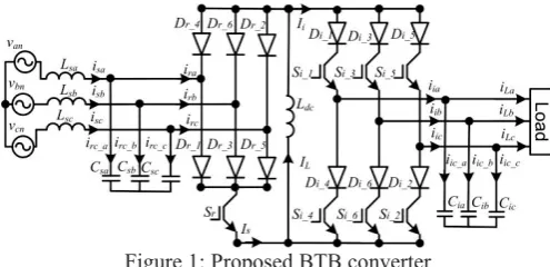
[image:3.595.129.288.303.392.2]The proposed BTB converter having the parameters listed in Table 1 is simulated. To demonstrate system soft start-up, the reference voltage at the load terminals is increased gradually from zero to rated voltage. To test the dynamic performance of the proposed BTB system, a load step change is applied at time t=1s by connecting an additional parallel resistive load of 18Ω. The results of these tests are shown in Figure 6 to Figure 10. Figure 6 shows that the voltage across the load is maintained constant at 311Vpk (220Vrms) as the load is varied.
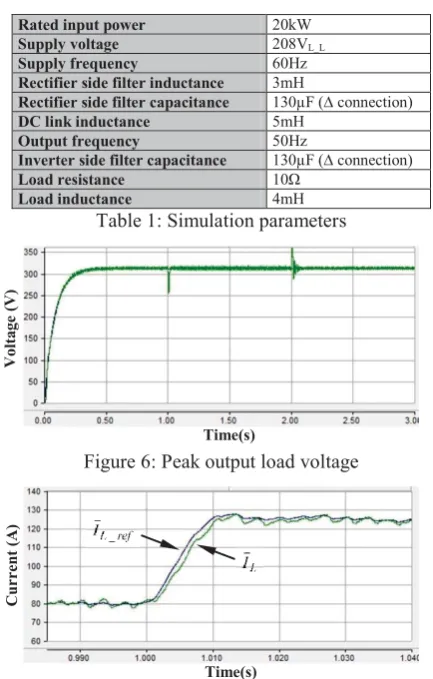
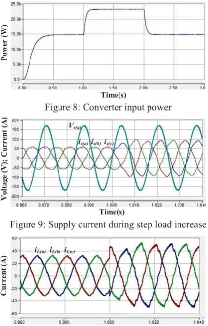
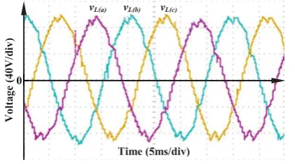
Figure 7 shows that as the load increases the average dc-link current and its reference (IതതതതതതL_ref) increase to maintain power balance between the ac and dc sides. Figure 8 shows that the step change in load causes the converter input power to increase from 15kW (0.75pu) to 23kW (1.15pu). Figure 9 shows supply currents and phase ‘a’ voltage as load varies, and highlights that the input power factor is in agreement with the theoretical values shown in Figure 4. Figure 10 shows the load current during the step change in load and highlights the proposed BTB converter’s ability to continue supply of sinusoidal current to the load.
Rated input power 20kW
Supply voltage 208VL_L
Supply frequency 60Hz
Rectifier side filter inductance 3mH
Rectifier side filter capacitance 130μF (∆ connection)
DC link inductance 5mH
Output frequency 50Hz
Inverter side filter capacitance 130μF (∆ connection)
Load resistance 10Ω
[image:3.595.317.534.408.748.2]Load inductance 4mH
Table 1: Simulation parameters
Figure 6: Peak output load voltage
Figure 7: Average dc-link inductor current during load step 0
0.1 0.2 0.3 0.4 0.5 0.6 0.7 0.8 0.9 1
0 0.1 0.2 0.3 0.4 0.5 0.6 0.7 0.8 0.9 1 1.1 1.2
Po
w
er Fa
ct
or
Input Power (pu)
Time(s)
Vo
lt
age
(V)
Time(s)
C
urren
t (
A
[image:3.595.63.268.476.613.2]Figure 8: Converter input power
[image:4.595.314.528.158.404.2]Figure 9: Supply current during step load increase
Figure 10: Load current during step load increase
4 Experimental validation
Results obtained from a scaled-down experimental test rig of the proposed BTB, with parameters listed in Table 2, are presented. Unlike with the simulation described in Section 3, the output voltage reference is changed to initiate a step change in the load. To enable soft start-up and soft change, the reference voltage is passed through a low-pass filter with cut-off frequency of 2Hz. Initially the output voltage reference is set to 75Vpk and then increased to 90Vpk,
corresponding to measured input powers of 380W and 840W respectively. Figure 11 and Figure 12 show the three-phase supply currents and phase ‘a’ voltage with output voltage references of 75Vpk and 90Vpk respectively. These figures
show that the supply currents are sinusoidal and that power factor changes from 0.8 leading to unity as the reference is increased. Figure 13 and Figure 14 show load voltage build-up during black-start and during a change in load voltage reference, demonstrating the ability of the proposed BTB power conversion system to operate in islanding mode. Figure 15 shows that the current source converter presents sinusoidal output voltages to the load.
5 Conclusions
A new current source based back-to-back power conversion topology for medium voltage applications is presented.
Theoretical analysis, simulations, and experimental results have shown that the proposed power conversion system offers several advantages such as soft start-up and shutdown, high efficiency, and fast dynamic performance. The presented ac side filter design ensures high power factor at rated power, and low input current THD at the rectifier side.
Rated input power 840W
Supply voltage 50VL_L
Supply frequency 50Hz
Rectifier side filter inductance 5mH
Rectifier side filter capacitance 120μF (∆ connection)
DC-link inductance 5mH
Output frequency 50Hz
Inverter side filter capacitance 90μF (∆ connection)
Load resistance 25Ω
Load inductance 3.3mH
Table 2: Experimental parameters
Figure 11: Detailed view of three-phase supply currents and
[image:4.595.317.524.448.567.2]phase ‘a’ voltage when output voltage reference is 75Vpk
Figure 12: Detailed view of three-phase supply currents and
phase ‘a’ voltage when output voltage reference is 90Vpk
Figure 13: Output voltage during start up
Time(s)
Po
w
er
(W)
Vs(a)
is(a) is(b) is(c)
Time(s)
Vo
lt
age
(V); Cur
re
nt (A)
iL(a) iL(b) iL(c)
Time(s)
C
urren
t (
A
) 0
Time (5ms/div)
V
olt
ag
e (
40V
/d
iv)
; C
ur
ren
t (
10A
/d
iv
)
Vs(a)
is(a) is(b) is(c)
0
Time (5ms/div)
V
olt
ag
e (
40V
/d
iv)
; C
ur
ren
t (
10A
/d
iv
)
Vs(a)
is(a) is(b) is(c)
0
Time (50ms/div)
V
olt
ag
e (
40V
/d
iv)
[image:4.595.319.523.620.731.2]Figure 14: Output voltage during an increase in reference
Figure 15: Detailed view of three-phase output voltage following an increase in reference
References
[1] L. Rixin, W. Fei, R. Burgos, P. Yunqing, D. Boroyevich, W. Bingsen, T. A. Lipo, V. D. Immanuel, and K. J. Karimi, "A Systematic Topology Evaluation Methodology for High-Density Three-Phase PWM AC-AC Converters," Power Electronics, IEEE
Transactions on, vol. 23, pp. 2665-2680, 2008.
[2] J. W. Kolar, T. Friedli, J. Rodriguez, and P. W. Wheeler, "Review of Three-Phase PWM AC-AC Converter Topologies," Industrial Electronics, IEEE
Transactions on, vol. 58, pp. 4988-5006, 2011.
[3] J. Alcala, E. Barcenas, and V. Cardenas, "Practical methods for tuning PI controllers in the DC-link voltage loop in Back-to-Back power converters," in
Power Electronics Congress (CIEP), pp 46-52,
2010.
[4] U. I. Dayaratne, S. B. Tennakoon, N. Y. A. Shammas, and J. S. Knight, "Investigation of variable DC link voltage operation of a PMSG based wind turbine with fully rated converters at steady state," in Power Electronics and Applications (EPE 2011), Proceedings of the 2011-14th European
Conference on, pp. 1-10, 2011.
[5] P. Tenca, A. A. Rockhill, T. A. Lipo, and P. Tricoli, "Current Source Topology for Wind Turbines With Decreased Mains Current Harmonics, Further Reducible via Functional Minimization," Power
Electronics, IEEE Transactions on, vol. 23, pp.
1143-1155, 2008.
[6] D. Jingya, X. Dewei, W. Bin, N. R. Zargari, and L. Yongqiang, "Dynamic performance analysis and improvements of a current source converter based PMSM wind energy system," in Power Electronics
Specialists Conference, 2008. PESC 2008. IEEE,
2008, pp. 99-105.
[7] T. Longcheng, L. Yaohua, L. Congwei, and W. Ping, "An improved control strategy for the current source back-to-back converters," in Electrical Machines and Systems, 2008. ICEMS 2008. International
Conference on, 2008, pp. 1985-1989.
[8] D. G. Holmes and T. A. Lipo, Pulse Width Modulation for Power Converters: Principles and
Practice: John Wiley & Sons, 2003.
[9] M. Tomasini, R. Feldman, P. Wheeler, and J. C. Clare, "Input filter pre-charge scheme for high-power PWM-current source rectifiers connected to a weak utility supply," Power Electronics, IET, vol. 5, pp. 215-220, 2012.
[10] B. Wu, High-Power Converters and AC Drives: Wiley, 2006.
0
Time (50ms/div)
0
V
olt
ag
e (
40V
/d
iv)
vL(a) vL(b) vL(c)
0
Time (5ms/div)
0
V
olt
ag
e (
40V
/d
iv)
[image:5.595.64.275.236.353.2]