International Journal of Innovative Technology and Exploring Engineering (IJITEE) ISSN: 2278-3075, Volume-8 Issue-8, June, 2019
Design and Performance Analysis of Pentagon
Shaped Microstrip Patch Antenna
P A Nageswara Rao, YSukanya, P. Mallikarjuna Rao
Abstract: Integration of RF circuit components is required to make the antennas more compact and robust and is a trend in wireless application now-a-days. The micro strip antenna of patch variety is able to satisfy the requirement but the disadvantage is reduced gain and reduced band width. The gain has a range of 1-2 dB. So in order to increase the gain as well as band width, the substrate with low dielectric characteristics and higher thickness can be used. However, thickness increases surface waves. So, proper thickness of the substrate is required. This paper proposes a micro strip patch antenna based on a special design (pentagon) suitable for resonant frequencies in the range of 7.6 GHz to 7.9 GHz. So the analysis has been done by means ofAnsoft HFSS software V 17.0 by taking Rogers RT/Duroid 5880 (tm) as substrate material into consideration.Subsequently the gain, band width, radiation pattern and return loss has been evaluated with equivalent designs.
Index Terms: Microstrip patch antenna, Pentagon Shape, Gain, Bandwidth, Return loss, Radiation pattern.
I. OVERVIEW
The micro strip patch antenna was first suggested by Deschampsin 1953.Munson and Howell commercialized such antennas in two or three dimensions around 1970’s. Basically the patch antenna comprises a ground plane and a radiating patch separated by a substrate. The feed lines and radiating elements are etched on the substrate with photolithographic process [1]. An illustration of the micro strip patch antenna is revealed in fig. 1.
Fig.1: Microstrip patch antenna
Radiating patch can have different shapes like circular, square, elliptical, rectangular, pentagon,
Revised Manuscript Received on June 05, 2019
P A Nageswara Rao, Associate Professor presently working at GayatriVidyaParishad College for Degree and PG Courses, Rushikonda, Visakhapatnam.
YSukanya, Associate Professor presently working at Vignan’s Institute
of Information Technology, Duvvada,Visakhapatnam
P. Mallikarjuna Rao, Professor, Department of Electronics & Communication Engineering, presently working in Department of Electronics and Communication Engineering, College of Engineering (A), Andhra University, Visakhapatnam.
hexagonal and thin strip(dipole) as well as triangular. So the feeding can be done by using any one of the methods such as co-axial feed, line feed, CPW feed, inset feed, proximity coupling or aperture coupling[4, 7-9]. Two techniques of analysis are being used are cavity model and Transmission Line Model (TLM). Micro strip arrays cannot be used at high power levels as they are poor sources of radiation over a limited band of frequencies in wave guide and co-axial line. Santanu Kumar Behera & Y. Choukiker recommended a novel design based on Particle Swarm Optimization (PSO) along with MOM to obtain geometric parameters. A.Deshmukh & G.Kumar have proposed a flattened L-shaped patch antenna to get wide band. Further the band width of the above proposed antenna improved by 23.7% -24.43% by Z. M. Chen [2]. A satisfactory performance of the patch antenna is obtained by K. F. Lee [2] with a reduced size using U – slot. S. C. Gao [2] used photonic band gap to enhance gain and band width.
II. PRINCIPLE OF WORKING
The working theory of micro strip patch antenna is explained as follows. The two sides of the substrate have maximum and minimum electric fields with the middle portion having zero value. With respect to the instantaneous phase of the functional signal, the field signs on the sides of the patch change continuously. Finally, there is a spread of Electric field towards the boundary so that TM10 mode is
radiated for rectangular patch.
Fr of patch antenna depends on the parameters like 1. Size of the GND plane 2. Patch width (impedance) 3. Thickness and εr of substrate. Applications of patch antenna include
global positioning systems (GPS), vehicle based satellite link etc.
M. Abbaspour and H. R. Hassani suggested star shaped patch antenna to enhance impedance bandwidth. Different shapes of patch antenna in support of X band applications are made with FR4 (Flame Retardant) Epoxy substrate proposed by Sumanpreet Kaur Sidhu, Jagtar Singh Sivia [3]. By using pentagon shape it can be proved that the band width is better in comparison with other shapes. More over return loss also gives advantage for pentagon shape.
III. DESIGN OF ANTENNA
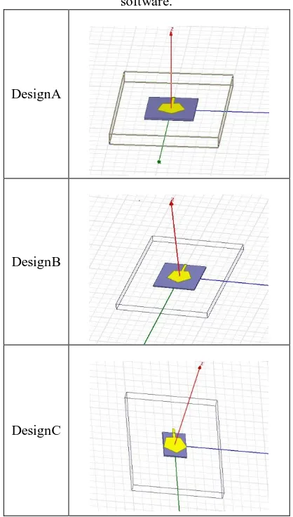
Table 1 displays the substrate measurements projected for three pentagon Microstrip patch designs [5, 6].
Table 1: Substrate Measurements
KIND X (mm) Y (mm) Z(mm)
Design A 100 90 3
Design B 100 90 3
Design C 75 50 3
Patch width (mm), respective resonant frequency - fr
(GHz) & the antenna designs simulated in Ansoft HFSS are provided in Tables 2 & 3 respectively.
Table 2: Patch width and fr of projected antenna
KIND WIDTH PATCH
(MM) FR(GHZ)
Design A 26.28 7.9
Design B 26.86 7.8
[image:2.595.64.273.353.721.2]Design C 26.86 7.6
Table 3: The projected antenna designs using Ansoft HFSS software.
DesignA
DesignB
DesignC
DESIGN EQUATIONS:
1. The width of the patch is calculated from,
Where, = Width of the patch = Speed of light
= value of the dielectric substrate
2. The value of the effective dielectric constant (ɛreff) is
evaluated from,
3. The length (L) isevaluated from,
4. The increase in size of the antenna due to fringing is determined from,
,
Where ‘ ’= height of the substrate
5. The characteristic impedance can be written as,
6. Ground plane length and ground plane width are given are calculated by,
7. Height of a substrate is given by,
8. Feed line length is obtained by,
, Where, = is guided wavelength
IV. SIMULATION RESULTS
The characteristic like gain, band width, return loss, and radiation pattern are discussed in this paper for the projected antenna. The impedance mismatch is measured by return loss. The bandwidth states the frequency range over which standing wave ratio is less than 2 which is a permissible level for practical applications. At a constant distance from the antenna, the power radiated as function of direction describes radiation pattern. Gain of an antenna is defined with respect to a reference antenna, which may be either λ/2 antenna or isotropic antenna and this method is called technically as gain transfer method
Table 4 shows the results obtained for Design A.The return loss graph for Design A is shownin Fig. 2. From the graph it can be observed that the minimum return loss is -24.34 dB at fr of 7.9 GHz. Fig. 3 and 4 shows the gain plot
International Journal of Innovative Technology and Exploring Engineering (IJITEE) ISSN: 2278-3075, Volume-8 Issue-8, June, 2019 Table 4: Design A outcomes
Characteristic Obtained Values
fr (GHz) 7.9
Return Loss (dB) -24.34
Gain (dB) 7.41
Band-Width (GHz) 7.62-8.12
Fig. 2: Design A – Return loss plot
Fig. 3: Design A – Gain plot
Fig. 4: Design A - Radiation pattern plot
The outcomes found from Design B are presented in table 5. Fig. 5 shows return loss plot having the least return loss of -18.79 dB at fr of 7.8 GHz. The gain plot and radiation
pattern found for Design Barepresented in Fig. 6 and Fig. 7.
Table 5: Design B outcomes
Characteristic Obtained Values
fr (GHz ) 7.8
Return Loss (dB) -18.79
Gain (dB) 7.67
Band-Width (GHz) 7.47-8.34
Fig. 5: Design B - Return loss plot
Fig. 6: Design B - Gain plot
Fig. 7: Radiation pattern of Design B
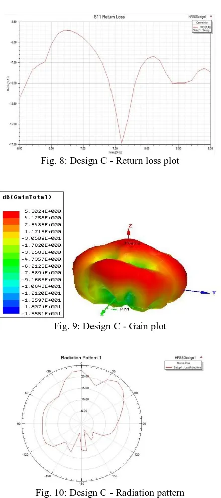
Table 6 displays the outcomes found from Design C. The least return loss of -17.33 dB at fr of 7.6 GHz is obtained
from return loss plot shown in Fig. 8. The gain is obtained as 5.60 dB from gain plot shown in Fig. 9. Fig. 10 shows the radiation pattern found for Design C.
Table 6: outcomes for Design C Characteristic Obtained Values
fr (GHz ) 7.6
Return Loss (dB) -17.33
Gain (dB) 5.60
Fig. 8: Design C - Return loss plot
Fig. 9: Design C - Gain plot
Fig. 10: Design C - Radiation pattern
The following Table 7 shows [10] the comparison for Design A, Design B and Design C obtained for resonant frequencies 7.9 GHz, 7.8 GHz and 7.6 GHz respectively in which Microstrip line feed technique is used and Roger’s RT/Duroid 5880 (tm) as substrate materials for all the designs. Design Bfor fr of 7.8 GHz gives the better
performance compared to other two proposed antenna designs.
Table 7: Comparison of Results for Design A, Design B and Design C
Characteristics Design A Design B Design C
fr (GHz) 7.9 7.8 7.6
Return loss (dB) -24.34 -18.79 -17.33
Gain (dB) 7.41 7.67 5.60
Bandwidth (GHz) 0.5 0.87 0.5
V. CONCLUSION
From the above results, Design B is capable with better results with fr of 7.8 GHz, gain of 7.67 dB and bandwidth of
0.87 MHz. Design A gives a bandwidth of 0.5 MHz and gain of 7.41 dB at fr of 7.9 GHz and Design C gives a gain
of 5.60 dB and bandwidth of 0.5MHz at fr of 7.6GHz, which
gives low performance characteristics when compared to Design B proposed antennas.
REFERENCES
1. Constantine, A. Balanis, “Antenna Theory Analysis and Design” 2nd
Edition, Wiley India (p.) Ltd., 2007.
2. L. Chandiea, K. Anusudha. "Pentagon shaped microstrip patch
antenna with metamaterial for UWB application", 2016 International Conference on Control, Instrumentation, Communication and Computational Technologies (ICCICCT), 2016
3. M. Abbaspour and H. R. Hassani, ”Wideband star-shaped microstrip
patch antenna”, Progress InElectromagnetics Research Letters, Vol. 1, 61–68, 2008.
4. Sumanpreet Kaur Sidhu, Jagtar Singh Sivia, “Comparison of
Different Types of Microstrip Patch Antennas”, International Conference onAdvancements in Engineering and Technology(ICAET 2015), International Journal of Computer Applications (0975 – 8887).
5. AnkurKaushal, SachinTyagi, “Microstrip patch antenna its types,
merits demerits and itsApplications”, International Journal of Engineering Sciences and Research Technology, pp. 619-622,2015.
6. Abhishek Joshi and Rahul Singhal, “Gain Improvement in Polygonal
Patch Antennas”, IEEEINDICON 2015 1570187331.
7. L. Chandiea and K. Anusudha, “Performance Analysis of Pentagon
Shaped Microstrip Patch Antenna”, IEEE International Conference on Computer, Communication, and Signal Processing (ICCCSP-2017).
8. Qurratul Ayn, P.A. Nageswar Rao, P. Mallikarjuna Rao, “Design and
Analysis of High Gain 2x1 and 4x1 Circular Patch Antenna Arrays for 2.4 GHz Applications”, International Journal of Innovative Research in Science, Engineering and Technology,Vol. 6, Issue 8, pp 16432 – 16439, August 2017.
9. P. A. Nageswara Rao, Qurratul Ayn, Y. Sukanya& P. Mallikarjuna Rao, “Design and Analysis of High Gain 2x2 Circular Patch Antenna Array With and Without Air-gap for WLAN Applications”, Journal of Advanced Research in Dynamical and Control Systems, Vol. 9, Issue 3, pp 258-271, October 2017.
10. Qurratul Ayn, P. A. Nageswara Rao, P. Mallikarjuna Rao & B. Siva
Prasad, “Design and Analysis of High Gain 2x2 Circular Patch Antenna Array With and Without Air-gap for WLAN Applications”, International ConferenceSPACES-2018, pp 41-44, 4-5 January 2018, KL Deemed to be University. *Added to IEEE Xplore Digital Library
on 15.03.218; DOI:10.1109/SPACES.2018.8316312.
11. Ch.Manohar Kumar, NVSS Kumar Muvvala “Effect of Metamaterial
on a Triangle Shaped Multi-Band Patch Antenna ”, Journal of Emerging Technologies and Innovative Research, Vol 6, Issue 3 March 2019.
12. S Krishna Veni1, G S K Gayatridevi “Design and Comparison of
Microstrip Patch Antennas for Wireless Body Area Network”, International Journal of Engineering & Technology, 7 (4.7) (2018) 167-170.
AUTHORS PROFILE
Dr. P. A. Nageswara Rao is an Associate Professor presently working at GayatriVidyaParishad College for Degree and PG Courses, Rushikonda, Visakhapatnam. He has obtained Ph.D in 2016, ME in 2003 and BE in 2000. He has 18 years of teaching experience at various Engineering Colleges. He has 17
research Publications in International journals/National journals,
[image:4.595.63.276.58.264.2]International Journal of Innovative Technology and Exploring Engineering (IJITEE) ISSN: 2278-3075, Volume-8 Issue-8, June, 2019 Mrs. Y. Sukanya is an Associate Professor
presently working at Vignan’s Institute of Information
Technology, Duvvada,Visakhapatnam. She is
presently pursuing Ph.D from GITAM University at Visakhapatnam, obtained M.Techin 2008 and BE in 2001. She has 11 years of teaching experience. She has 11 research Publications in International journals/National journals, Conferences and Proceedings to her credit. Her area of interest includes Antennas and Signal Processing.
Mallikarjuna Rao Prudhiviis a Professor,
Department of Electronics & Communication
Engineering, presently working in Department of Electronics and Communication Engineering, College
of Engineering (A), Andhra University,
Visakhapatnam. He has 33 years of teaching experience. He obtained Ph.D. in 1998, ME in 1986 and BE in 1982. 12 research scholars have been awarded Ph.Ds under his guidance from various reputed Universities and presently guiding 6 Ph.D scholars. He has
more than 100 research Publications in various International
journals/National journals, Conferences and Proceedings in his credit. He
has been awarded the best Ph.D. Thesis Award (Gold Medal from the