International Journal of Innovative Technology and Exploring Engineering (IJITEE) ISSN: 2278-3075, Volume-8 Issue-7, May, 2019
Abstract: Hierarchy multiplication is desirable since of its capacity to carry the multiplications with high speed. An approach of implementation of hierarchy multiplier involves utilization of array multiplier. A drawback of array multiplier is that it has a critical delay path. In order to overcome this problem, a new methodology has been proposed in this paper which replaces the array multiplier with a Vedic multiplier. In Vedic multiplier ‘Urdhava-tiryakbhyam’ sutra makes the partial products and erase the unnecessary multiplication steps. The methodology has been implemented in mentor graphics tool using 45nm technology. From the simulation results, the proposed methodology reduces the area and delay when compare to the different existing designs
Index Terms:Vedic Multiplication, array multiplication, carry save adder, hierarchy multiplier .
I. INTRODUCTION
Multiplier is major arithmetic process in Signal Processing application of a Cryptography, error correction and microprocessors. Depending on time intense for the multiplication process it decided performance of classification. The basic multiplier has to design high speed basic multiplier [1].
The array multiplication starts from the increase parallelogram. In Each phase of parallel adders should get some partial product inputs and the carry-out is circulated into the following rows.
In array Multiplier the regular shape and minimum complexity are the advantage and more critical delay and partial products are the disadvantage.
Wallace multiplication and the multiplication products are summation of similar by technique for a multiplication of carry save adders. [13].The advantage of Wallace multiplication is having less partial products when compare to the array multiplication.
The main disadvantages of Wallace multiplication is high delay when compare to that of booth multiplication. The Booth algorithm is the most habitually utilized technique to create intermediate partial products and speed gained by skipping 1’s depends on the data. This process takes into explanation the reduction of number of partial products to be occupied in a carry save adder. Advantage of Booth
Revised Manuscript Received on May 10 ,2019
D. Naveen Sai, Electronics and communication, Koneru Lakshmaiah Education Foundation, Guntur, India.
Damarla Paradhasaradhi Electronics and communication, Koneru Lakshmaiah Education Foundation, Vijayawada, India.
Dr.R.S.Ernest Ravindran Electronics and communication, Koneru
multiplication advantage is to decrease general product and speed up operation. The main disadvantage of booth multiplication is partial products are more. To overcome this drawback the hierarchy multiplier will be speed up their operation.
Section II gives detailed explanation of hierarchy multiplier and Array multiplication Section III explains the Vedic Multiplication and carry save adder. Results and the discussion are explain in the section IV. Section V concludes the paper.
II.EXISTINGMETHOD
Speed is determined from the estimating the delay of base multiplication. In hierarchy multiplier delay can reduced by minimalizing the sum without upsetting the functionality. The subsequent methodology reduce the delay in hierarchy multiplication.
Step1: The multiplier information input are presented as A, B and output C.
Step 2: Divided the n bit multiplication input sources i.e., A and B, equivalent two half. For input source A, is separated (An/2 — 1... Ao), (A... An/2), allocated AL and AH, separately. A similar system is likewise `received for another multiplication input b.
Step 3: Subsequent to separating equally the input sources, are shaped into 4 parts like (AL, BL), (AH, BL), (AL, BH) & (AH, BH).
Step 4: The basic multiplication consists of four blocks, X0, X1, X2 and X3.
Step 5: Multiplication produce bit are yn/4 — 1, yo is acquired from 0 to n/2-1 output bits of Xo.
Step6: Resultant bits of a1, a2 and connection of a0 (n/2 To n), a3 (0 To n/2-1) are held at via carry save adder According to stage 6, which thusly handled via carry save adder in this manner consequences into 2 columns of 8 bits output source. Step7: The inputs for ripple carry adder of n bit adder. Likewise, the aggregate output of the Carry select adder allotted to the multiplication subsequent bits for the range of yn + n/2 — 1… yn/2.
Step 8: Binary Excess Converter takes the source from X3 (n/2 To n bits) and the source output are accessible before ripple carry adder and they are passed to multiplication. Step 9: The multiplication source output bit are y2n ... yn + n/2 acquired from the multiplexer, in view of the carry output of ripple carry adder, in the event that it is hone, at that point the Binary excess one converter output source are turning into the output generally the item bits of a3 (n/2 to n bit).
Comparative Analysis of
Efficient Hierarchy
Multiplier using Vedic Mathematics
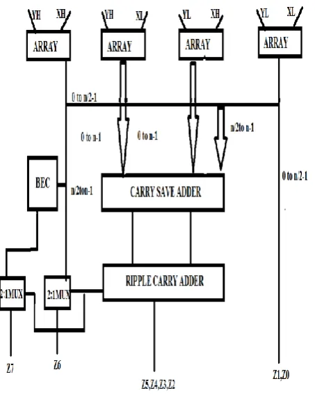
Another contribution for the multiplexer is from a3 output .At long last, the multiplication chooses, binary excess one converter or a3 source input as y7- y6, in view RCA .In existing design the hierarchy multi-plier consists of array multiplier, binary excess one converter as shown in the fig 1.
Fig 1: Existing Hierarchy Multiplier
Array multiplier
[image:2.595.314.533.54.260.2]The array multiplication includes adding of multiplicand bits and multiplier for the generation of partial products. In second stage half adders has been utilized for the decrease of created incomplete items in two columns. Followed by addition of two rows utilizing adders in the third stage as shown in fig 2.
Fig 2: Array Multiplication
Binary excess 1 converter
Binary excess one converter (BEC) to rise the speediness of procedure. This logic operation can be performed with the adder to that additionally improve the speed. It can accomplish low area and power utilization, [7-9]. Excess one converter is acquired by adding one to binary values. The Binary excess converter the n bit input bits and the n bit output bits; whereas Binary excess one converter with carry input and produces n+1 outputs and given the carry output as the choice contribution of the following stage mux utilized in the last adder structure and binary excess one as shown in fig 3.
Fig 3: Binary Excess 1 Converter
Carry save adder
[image:2.595.59.286.123.407.2]International Journal of Innovative Technology and Exploring Engineering (IJITEE) ISSN: 2278-3075, Volume-8 Issue-7, May, 2019
III.PROPOSEDMETHOD
The minimum delay of hierarchy multiplier is implemented by n number of bits. For illustration, the work for 4 bit multiplier design is clarified.
Proposed design 1:
In the proposed design there will be having Vedic multiplication and the Carry Save Adder. Proposed design one as shown in the fig 4.
Fig.4: proposed design Include Vedic multiplication, CSA and RCA
Vedic multiplication:
Vedic Multiplication is discussed about the dependence of UrdhvaTiryakbhyam Vertical and crossway are determined. Utilizing this sutras the fractional and summed are produced. Multiplication configuration has the satisfactory position that as the quantity of builds, the area & delay rises gradually. The two bit Vedic Multiplier is represented exhausting 2 half’s adders and 4 AND gates. Consider 2-bit binary numbers a0b0 and a1b1 as multiplicand and multiplier individually. To start with, the least huge bits of the multiplicand multiplier are increased vertically as appeared in Fig 5.
Fig.5: Vedic multiplication algorithm
The obtained result will be stored at the last digits will be multiplied. The binary digit multiplication is extended the same way as shown in fig.6
Fig 6: Basic Multiplication Steps
10 * 11 1 0 1 1 --- 1; 1+0; 0 = 110 (result)
Proposed design 2:
Fig.7: proposed design include Vedic multiplication, CSA and CSLA
Carry Select Adder
Carry select Adder produces the possible of two input of C (1 or 0). It produces the outputs sum and carry ahead of time which finished by utilizing 2 ripple carry adders of carry determination to be zero or one is finished and assistance of the multiplication. The carry select adder together contains two RCA and a multiplexer, each gathering of the ripple carry adders are connected to the full adder.
IV.RESULTSANDDISCUSSION
The proposed design that can be implemented in mentor graphics tool by using the 45nm technology simulated outcomes 4-bits hierarchy multiplication and basic elements are, 2-bit Vedic multiplication carry save adder, 2 bit binary excess converter and 2:1 mux. Enactment constraints, such as power consumption, area consumed and Power delay product of the simulated design with a source voltage with one volt.
Table 1: comparative analysis of hierarchy multiplier
Design specfication
Power(µm) Area (T)
Delay (nm)
Existing[5] 43.32 337 59.52
Existing Design 28.32 450 119.32
ProposedDesign 1 19.29 314 99.16
ProposedDesign 2 11.79 210 49.19
.
Graphical reprensation of Table 1.
International Journal of Innovative Technology and Exploring Engineering (IJITEE) ISSN: 2278-3075, Volume-8 Issue-7, May, 2019
Author-1
Phot
o
Fig no: 4X4 hierarchy multilier wave form
V.CONCLUSION
The proposed architecture is Vedic multiplier it is based on the ‘Urdhava-tiryakbhyam’ sutra it is general multiplication technique. The area is increased and delay is less with the number of bits by the Urdhava-tiryakbhyam’. Further this Vedic multiplication can be designed in gate diffusion logic
(GDI) and finfet technology.
REFERENCES
1. Mohan Shoba and Rangswamy Najera, Energy and Area Efficient Hierarchy Multipliers Architecture based on Vedic Mathematises and GDI logic , Eng Scien & Tech, an Inter Jorn (2016)
2. Sri.Phani Ramya.SNimmy Maria Jose , A Low Power Binary to Excess-1 Code Converter Using GDI Tech, ijareeie ,Vol. 4, Issue 1, January 2015 3. Banish Bennet and Dr.sMaflin, modified effi-cient carry save adder, intend
Conf on Circuit, Power and Comp Tech [ICCPCT], 2015
4. Sri-kanth, IThahiraBanu and G.VishnuPriya, Low Power Array Multiplier Using Modified Full Adder, 2nd IEEE Inter Confec on Eng and Tech (ICETECH), 17th & 18th March 2016, Coimba-tore, TN, India. 5. Nagaraj, GM.Srerama Reddy and S.r.Aruna Mastani, Analysises of the
different Adder using Dpl logic, 978-1-5386-4318-1/17/$31.00 ©2017 IEEE
6. Bhavana.Koada, Meghaana,2 Md.Omeair Jaleel3 and Pranet Raj Jerirpotula, a Comparative Study on Adder, 978-1-5090-4442-9/17/$31.00 c 2017 IEEE
7. Angina Sa,, Pradeep Ca , Philip Samuelb, Syn-thesizes of Speed Floating point of Multipliers Based on Vedic Multiplier, Inter Conf on Infor and Conf Tech (ICICT 2014).
8. G. Kishor Kumar and NBalaji, Reconfigurable Delay Optimized Carry Select Adder, Proceedings of IEEE Inter Confer on Innov in Elect, Elec, Inst and Media Tech ICIEEIMT 2017.
9. sa’ed abed1, bassam jamil mohd1, zaid al-bayati2 and sahel alouneh3, low power wallace multiplier design based on wide counter, int jour of circuit theory and applic. j. circ. theor. appl. (2011)
10. Keta masurkar & Pravin dakhole, implemen-tation of optimized Vedic multiplier using cmos technology, inter conf on conf & sig proc, apr 6_8, 2016
AUTHORSPROFILE
D. Naveen Sai currently pursuing his master’s degree in VLSI design at KLEF deemed to be university. He obtained his bachelor’s degree in electronics & communication engineering at RVR&JC. His working area of interest includes digital VLSI design and Nano electronics.
Damarla Paradhasaradhi, currently working as Assistant Professor in Koneru Lakshmaiah Education Foundation, Vaddeswaram, Guntur. He did M. Tech from Pondicherry University in 2014. He worked as an ASIC Design and Verification Engineer for 2 Years. His research interests are CMOS VLSI, QCA, MEMS.