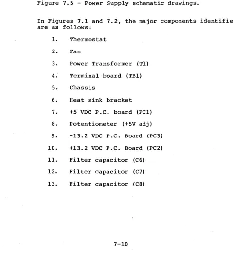
How to maintain the
CONSUL 980
ADDS
HO\N TO MAINTAIN THE
CONSUL SBD
TABLE OF CONTENTS
1. INTRODUCTION
2. THEORY OF OPERATION
3. GLOSSARY OF SIGNAL NAMES 4. UNIT TEST PROCEDURE
5. PHYSICAL ACCESS FOR TEST AND REPAIR
6. TROUBLE-SHOOTING CHART
7. POWER SUPPLY SUBASSEMBLY
8.; T.V. MONITOR SUBASSEMBLY
9. KEYBOARD SUBASSEMBLY
1. INTRODUCTION
This manual is intended for use by personnel who must perform fault diagnosis and repair of the Consul 980. The reader should be familiar with ADDS publication number 98-3000, HOW TO USE THE CONSUL 980, which presents complete operating instructions and interface information. Before proceeding with the Theory of Operation, salient terminal features are described below. 1.1 General Description
The Consul 980 is a low cost TTY compatible CRT display ter-minal. It is designed for users who wish to take advantage of a CRT's silent operation,. fast transmission speed and inherent reliability •. It is a self-contained desktop unit. The 980 displays data in a format of 24 lines with 80 charac-ter per line - making a total of 1920 characcharac-ters. Data is displayed as black characters on a white background. Com-munications with the data .processing system or a minicomputer
takes place a character at a time on a conversational basis, or in the form of message blocks.
1.2 Salient Terminal Features
EIA and Current Loop Interface
An EIA RS232C voltage interface and a 20 milliampere current loop interface are standard. Both are operational over the full speed range of the terminal up to 9600 baud.
Five Transmission Speeds
Transmission rates of 110, 300, 1200, 2400 or 9600 baud are selectable by means of a switch on the rear panel.
Half/Full Duplex
A DPDT switch on the rear panel permits selection of full or half duplex operation.
Cursor Control
Cursor controls to position the cursor up, down, forward, backward and home are available. Home is the lower left
corner in CONV mode, and upper left corner in non-conversation-al mode.
Hard Copy Interface
Allows attachment of a serial or parallel printer. The oper-ator can control the flow of data to the printers by using the PRINT ON, PRINT LOCAL and PRINT OFF keys on the 980 keyboard.
Audible Alarm
The BEL code causes an audible alarm in the 980 to be activated.
Remote Control .
The 980 is a completely remotely controllable terminal. The CPU can directly address any cursor position on the screen, insert or delete lihes, read the current cursor location, ring an audible alarm and control the flow of data to the peripherals.
Editing Features
The 980 has some powerful editing features. Besides the
five cursor movements mentioned, the 980 can insert/delete a character at a time or insert/delete an entire line of characters, do horizontal tabbing and erase the screen.
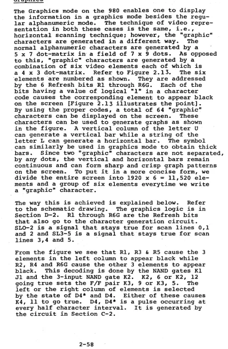
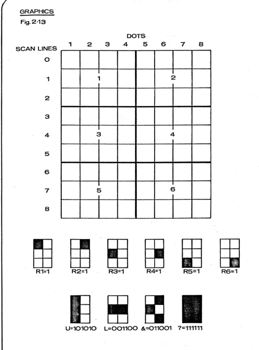
Graphics
A graphics capability is available on the 980 which
pro-vides a matrix of 11,520 "graphic" elements. These elements can be used to generate business-level graphs such as bar-charts and trend curves.
Formatting
A formatting feature which can be used in either the Page or Message mode permits simultaneous display of both fixed and
variable data. This feature not only makes data entry easier
1.3 General Specifications a) MEMORY Size:
b) SCREEN Size:
c) SCREEN PRESENTATION: # of lines
Character/Line Character size
Color
Character Set
Refresh Rate
d) COMMUNICATIONS INTERFACE: EIA
Current Loop
Mode Code Parity
1-3
1920 Characters 12" Diagonal
24 80
0.1" wide (Typ.) by 0.2" high (Typ.)
Black Characters on a a White background
96 Upper/Lower case ASCII characters
60 frames/second
Conforms to RS232C; operates at l10~ 300, 1200, 2400, 9600 baud
20 milliamperes; operates at 110,- 300, 1200, 2400 9600 baud
Full/Half Duplex USASCII
e) OPERATING MODES:
Conversational Message
Page
f) EDITING FEATURES:
g) WEIGHT:
h) PHYSICAL DIMENSIONS:
i) POWER:
j) TEMPERATURE:
k) HUMIDITY:
Character at a time Line at a time
Full screen at a time
Character and line insert/ delete, character overwrite, horizontal tabbing, cursor movements
52 lbs. maximum 21" x 14" x 23"
110V at 60 Hz, l65VA 220V at 50 Hz
2. THEORY OF OPERATION
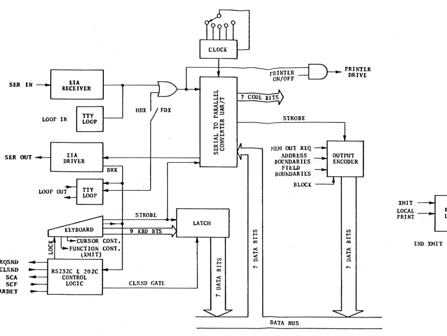
A block diagram overview of the Consul 980 electronics is presented in this section. I t is followed by a detailed circuit description at the circuit level.'
2.1 General Summary
2.1.1
2.1.2
The Consul 980 electronics package is made up of five basic
blocks. They are the Front End, the Control, the Memory,
the Video Generator and the Option. Each block is wholly
contained on one printed circuit card. A single
input/out-put data buss architecture is used to ease system design.
Front End
The Front End block contains the Universal Asynchronous Receiver/Transmitter (UAR/T), EIA level shifters, 20 rna current loop converters, keyboard interface, the RS232C control logic, the Output Encoder, the Read Logic and . the switch-selectable baud rate clock for asynchronous
communication.
Control
The Control block contains the code Decoder, the Cursor Control Logic, the Data Access Logic, the scroll logic
and the Transparent Mode Logic. It also contains the
master oscillator along with a divide, by 8 counter, the three character generators and the video shift register.
2.1.3 Memory
2.1.4
The Memory block contains the Display Buffer Memory and its associated 2-phase clock generator, the one line Refresh Buffer Memory, the access logic to control
input to the Display memory, the "look ahead" compression
logic and the output multiplexer. The buffer for the
parallel printer is also on this block.
Video Generator
The Video Generator contains the timing chain counters for controlling all video signals, the video amplifier and mixer, sync and blanking generator, display select and cursor. generators, the blink circuit, the 1 of 3 ROM's enable circuit, the Address 'Registers and the
Tracking Registers. I t also contains the multiplexer
to output the current cursor address.
2.1. 5 Option
This block contains all the options offered with the
Consul 980. These include line insert/delete, charachter
2.2 Block Diagram Description
The overall system block diagram Figure 2.1 shows the four major sections, the Front End, the Control, the Memory and the Video Generator, divided by dashed lines.
A single 7-bit wide data buss runs through the whole
system. All output data rides on this buss. The Front
End accepts this parallel data, converts it to serial data, and sends it out on the communication lines. All incoming data has to enter the system through the Front
End. The serial input data is converted to parallel data,
7-bit wide. These bits are then used on the Control, the
Memory and the Video Generator for specific purposes.
The Control section decodes the 7-bit data. Depending on whether i t is a control code or not it activates the Access and Control Logic, to perform the corresponding control function if it were a control code or to load the data into the Display Memory if it were a message character.
The Display Memory is modular in organization. It is made up of both dynamic and static shift registers whose contents
are continuously recirculated at a rate of 1.6 MHZ. The
entire Display Memory has a storage capacity of 1920 x 8 bits. The Display Memory feeds a Refresh Memory of 80 x 8
bit capacity. It provides the 6 refresh bits for the
character generator to generate a 5-dot pattern for every .scan line. A total of 7 such 5-dot patterns are required
2.2.1
to display a character on the screen. These 5-dot patterns
from the character generator are applied to the video mixer. Here it is mixed with other timing signals. The composite signal is then amplified and applied to the video monitor.
The 980 system consists of one more section - the Option
Card. It provides all the Options available on the Consul
980.
Front End
2.2.1.1 Input Data Path
Input data to the Front End can be either current loop or EIA serial data. The serial data stream
[Figure 2".2] is converted to TTL levels and applied
to the UAR/T which converts the serial data to ~rallel
data. The parallel data, together with a strobe pulse,
is presented to the decoding logic on the Control block. If the character is displayable it is also presented to the Display Buffer Memory on the Memory block. All illegal characters and RUBOUT are ignored by the CRT.
SER IN _____
EIA
D-
....JRECEIVER
o.o.l ....J....J <
a:
<
.
LOOP
IH TTY'-D::
IoiJ
LOOP
-
Of-f-a:
;JJ
HDX
FDX
....J><z
~o
~u
~
U)
SO
OUT ...
- - IEIA
BlIVER
--RQSND
--CLSND
-SCA
-SCF
--CAIDET
-- ..--:I11III ---'~ IQ
--LOOP
OUT-
...
TTYLOOP
~ ...STROB[
-
~...
LATCH
r---
~~~BOARD
7IBD BITS
J1;:
CURSOR CONT
y...,..----,..--..,I en___ . . _FU_'
NCTION CONT
f-o-
(XMIT)
;;
RSZ1ZC
Ii202C
CONTROL
LOGIC
~
CLSND GATE
<
f-o
< ~
7CODLBI~
Jo-~~-V
SYSll.M BLOCI( DIAGRAH - 980
fig.2·17 DISPLAY RITS
DECODE
LOGIC
-
HI:J.tORY
IHSPLAY
A~D5
ADDRLSS
B 11S
ADDRESS
BOUl\'DAR
IES ...
l FIELD
REFRESH
~t--_S_T_RO_B_E_r-__ ....
"""-_:~B~OU.;;..;N;..;,,;D;;,;;A..:;;.R.:..;;I;.;;:E:..::·S~_~_r-
_____
..J 6RLFRSII B1$
CllARACTLR
GENLltATOR
ADDRESS
BOUNDARY+" OUTPUT
ENCODER
DATA BUS
-y-~.--...---'
CLOCI(
ANI>
DECODING
LOGIC
r-CLK
UIG-,
~
CLK TNG
r
ADlJRESS
HEr.ISTER
TRACKING
RLGISTER
BLANKING
Ii
SYNC CIRCUIT
V HllO
~IIXER
CURSOR GEN
IiCONTROL LOGIC
~_CURSOR
CON1ROL
1 - - _ - " ___ -.1 V I D L 0
2.2.1.2
2.2.1.3
2.2.1.4
Output Data Path
Output data rides on a single 7-bit data buss. It is generated in one of the following ways: the key-board, the memory (during read operation), the out-put encoder (outout-putting the active control characters like LF, CR, SO, SI, GS, ESC, ETC) or in response to the external request for current cursor position. The ASCII code together with a strobe is then pre-sented in parallel, if proper conditions exist at the RS232C control logic, to the UAR/T for parallel to serial conversion. The serialized data is then converted from TTL levels to EIA levels, or current loop signals, and sent to the modem or the CPU. Full/Half Duplex Modes
Full/Half Duplex is controlled by a SPDT switch on the rear panel. In FOX, conversational mode the serial TTL output goes only to the level converters for output. In HDX mode the serial output data is also routed to the UAR/T. This causes the output charact-er to be treated as an input charactcharact-er from the CPu. RS232C Control Logic
This logic handles all the necessary control lines to and from the EIA connector. The first character of a message transmitted, or keyed out live in conversation mode, raises Request to Send. As soon as Clear to Send (from the CPU) goes true the character riding on the output buss is loaded into the UAR/T for trans-mission. The reverse channel signals SCF and SCA are also controlled by this logic.
2.2.2 Control
2.2.2.1 Decode Logic
The parallel data from the UAR/T on the Front End block is presented to the decoding logic on the control block
[Figure 2.3]. If the 7-bit code is a Control code i t is decoded into one of 17 control codes. These are then latched to form control functions, each perform-ing a specific task. All illegal control codes are ignored. ·.Non-Control characters are written into the memory.
S ER IN - - - 1 - -...
EIA
RECEIVER
Loor IN
TTYLOOP
SER OUT --_ ... [IA
DRIVER
-~ __________ ~ BRK
-
----LOOP
OUT TTY~
wor
-~
~j L.~CURSOR
CONT.
g
FUNCTION CONT •
...J lXl-1I T)
RQSND
-CLS~D
-
RS232C& 202C
SCA
-
-
CONTROL
SCF
.
LOGIC
CARDET --.
~
..---:
-HDX FDX
STROBL
to. 9
KBD BTS
.')
-y
CLSND GATE
FE/ASYNC llLOC~ DIAGJlA)"
Fig.
2,2----CLOCK
....--~ rRINTLR _
ON/OFF
.
...J
COOL BITO ~
7 ...J ....
...J'-;.2~ V
<::J
,;;..
c: STROBE
O~
...
c: ...J~
:S~
~o
IA
~u ttE~f OUT REQ -...
V)
N-
ADDRESS--
B01JNDARIES ---..FIELD
BOUt-tDAR I [S
~
BLOCK
LATCH
DATA
BUS---- PRINTER DRIVE
,
OUTPUT ENCODER•
"
X~fITLOCAL
_ - - . IrRINT
END DIlT
READ
LOGIC
READ
[image:13.1233.72.981.57.742.2]MASTER
CLOCK
12.521 MHz
+8
VIDEO BIT SHIFT
MEMORY CLOCKS
INTRACHARACTER TIl-tINGS
1\
1OF
3 AFRSH
BIT~ CllARACT~RliS
1S2
S
GENERATOR
~
6 R 4
CI)
i-o
I:Q
,U).?
LOA
D'..
1.566 t-Ulz
VIDEO
SHIFT REGISTER
SLR CIIAR
SHIFT C LK
-+
t..DECODE
. BITS
LATCH
LOGIC
r
1OF
17CONTROL
7
CODE
CODES
STROB
Et
STROBE
1,
•
STROBE 2
STROBE
ESCAPE
CONTROL BLOCK DIAGRAf.1
Fig.2·3-
--SPECIAL
CODE
LOGIC
.
LAST LINE
END OF LINE
SCREEN ERASE
STROBE
1STROBE 2
LINE FEED
COMPRESS
READ
.' DATA STROBE
SCROLL
INSERT/DEL
RESET ON POWER
--.
~
SCROLL
LOGIC
---.
t
•
I
~p
--
DATA
•
ACCESS
-..
LOGIC
-I
1
OF
5CURSOR
- - - - ' \ r - - - .COMMANDS
CURSOR
CONTROL
...
...-CONTROL
FUNCTIONS
LATCH DATA
ADDRESS COl-WARE
LOr. I C
t---.TAR CLOCK
HOR I ZONTAL ADDRESS _ _ _ _
...Jg2
SCROLL
.LINE ADVANCE
TERMINAL READY
LOAD DATA
LATcn DATA
LOAD SPACL
1
OF
5CURSOR CONTROLS
2.2.2.2
2.2.2.3
2.2.2.4
Access Control
The Access Control accepts the control functions from the decoder, and performs the task requested. These tasks include data input, erase functions and scrolling.
Cursor Control Logic
This logic accepts 1 of 5 cursor commands from the keyboard and causes the corresponding cursor move-ments. I t also handles horizontal addressing and tab functions.
Character Generator
The character generator accepts one character at a time from the Refresh Memory and then outputs the proper portion of the character to be displayed.
The line of characters in the Refresh Memory is presented to the generator seven times to complete the display of that data line.
2.2.3 Memory
2.2.3.1
2.2.3.2
2.2.3.3
Display Buffer
The Display Buffer memory is composed of shift regist-ers that recirculate their contents at a 1.6 MHz
Shift rate. The memory is modular [Figure 2.4] in that i t is divided into three sections. Each section has a capacity of 5120 bits or 640 8-bit characters. Refresh Buffer
This is made up of a static shift register which has a capacity to hold lOO.8-bit characters. However, only 80 characters of a particular data line are used for display. The Refresh Buffer holds one line of characters during the time the character generator is generating that particular line of data on the Consul screen. It is updated after every 9th scan line or at the end of every logic line by one of the 640 character modules.
Compression Logic
-
CIC SPACE 3 - - - ,~
SPACE 2..3
e
SPACE 1DATA 1
11
..
DATA
2
v
~
DATA 2"
11
-.A • DISPLAY BITS .,
1
DATA
3'
Y
DATA3'
~
DATA
~
..
,
RFa5H DATA"
t '
MEMORY 1
INPUT }tlJLTI PLEXER
.fEMORY 2 INPUT .IJLTI FLEXER
MEMORY 3 INPUT MULTIPLEXER
V£--r-r-.,-.,.-____
J.O.AD 1 _ _
1
LOAD 2
-LOAD 3
---...0
SCROLL
-~
-V
~ v,
V
DISPLAY 1-IDI
8 x 640 8 x 1
8 x 640 8 x 1
• x 640 8 x 1
MEMORY BLOCK DIAGRMI Fig.2·4
-'\
DATA 1 )
v
DATA
2""
,;
DATA 3 ,i
v
--
r
~
4( :.J
...
u<
'-Q~
~8
lila:
....
>-u
4(~..;a a:
Co
III
~
Q
TRANSFER (SCAN LINE 8)
I'
RFRSH DATA~
~
REFRESHMEt-tORY
-V
8x80•
INPUT
I--IRFRSH BTS
RFRESII . CLOCK
READ - - - - I ...
1
1:---
DISPLAY SPACE CODEj •
,
DELETE SPACE ' - - - - INS/DEL CLOCI
Mat CLOC~ ~ Mal CLOCK
GENERATOR ENABLE
4
,
,1
'2
8 MEM IITS
A
B
SELECT CLOCKS
- - - - MEM DATA ENABLE
-'-
DATA LAT CHc:x: ~
... t&1
2~
UTCH...
8~
-
ISPLAY DTS' .A.I
7 D
i
DATA BUS
STR
..
INPUT ACCESS
A
..
LOGICB
...
,
l
COMPRESS t--... CO}tIPRESS
LOGIC
A.
IUFFER . 7HC BITS
r
·
·
----.
·
...·
...·
LOAD 3 LOAD Z
LOAD 1
SPACE 1
SPACE 2
SPACE 3
2.2.3.4
If the remainder of the current line is blank, (i.e., filled with SPACE codes), one space code is output and the line is then terminated by
send-ing the proper codes. If in Page mode, the next
line is output following the CR/LF codes. If in
message, the transmission is terminated with a CR.
Output Multiplexer
During transmission this circuit accepts data from the memories and outputs i t on the data buss through a tri-state latch.
2.2.4 Video Generator
2.2.4.1
2.2.4.2
2.2.4.3
Clock and Timing Chain
This consists of the Master clock followed by a countdown chain and its associated decoding logic
[Figure 2.5]. This chain generates all the timing signals required for video presentation and memory timing.
Video Amplifier , Mixer
The blank and sync signals and the video display signals are mixed by the mixer to form composite
signals. These are then amplified by the amplifier
to the level required to drive the CRT.
Address Register
The Address Register contains the address of the loca~ion in which a character may be entered into or fetched from the Display Memory module.
2.2.4.4 Tracking Register
.The Tracking Register tracks the Memory Registers by
counting the shift pulses to the Display Memory. Its
contents at any given time represents the ~ddress of
the.memory location that is available for access.
2.2.5 Option
2.2.5.1 Insert/Delete Logic
1.566 MHz
aJltSOR .--..
fORlWlJ)
OJIlSOIt-..
BAClIWlD
':"100 •
liB LAN l:
UDRIVE
IISYNC
15.6 (lIz
CHARACTER DECODE
DECADE
0-9 a
CQ~It--~t~
__
- r __ r -____ ~4·ZERO
--1.74 (lIz
.!..9
•
VIDGEN BLOCK
Dl~GRAMFig. 2'5
-.!.. 29 60 HZ
FRAME RESET
•
LINE DECODES
VBLANK
VDRIVE
BINARY
0-7
}.IE}'I DISPLAY SELECT
5 ADDRESS BITS
~3~
~27
BINARY
0-7
.
LINE ZERO
----4j~j
---t--+---.J'
4
LOAD LI NE
---4---I--+---_~BINARY
0-2
LATCH
1 - - - - . 1
-
A
1--... B
SER· CHAR
HILANI
VBLANI:
6 RFR DTS
COMPOSITE
SYNC
GENERATOR
MIXER
COMPARATOR
-
COMPAIATOR
r--COMPARATOR ..-...,-_
-- COMPARE
LINE
SLO I L N I
-fAST
ILNI _ _ -oJHALF INT
-OIARAC1'ER - - - I ...
CLOCI
DECADE 0-9BINAltY
0.-7
BINARY
0-7
ADDRESS
COJ.IPARE
CIIARACTER ____
COONT
LINE ____
COUNT
CURSOR. _ _ _
----JCUPH _ _ _ _ ----J
MULTIPLEXER
DATA BUS
COMPOSITE
DISPLAY
SELECT
CEN
1--... _
SECT
11--.... - S~CT 2
INTERNAL
I---I-~HDRIVE
VIDEO
DRIVE
GEN
1---1.- VOltIVE
v-~~ _---~
VIDEO
VIDEO
>-e--....INTERNAL
VIDEO
TOME'"
SYNC
CURSOR
GEN
BLINICIRCUIT
1--4~}'lEM
CLOCK
•
ENABLE
1--...
CUItSOR
...-. ... -;.- 5 La
BLNI
1---11.-
FAST BLNl
.
1--.... - HALF
INT
1--4~
ROM 1
IOF 3 ROM
ENABLE 1---1 ... ROJ.I 2
CIRCUIT
I---t-_~
ROM 3
OPTION
CAJlD BLOCK DIAGR»' Fig.2.6..---~
LI HE LONG
TTY
f--t--~
LOOr
LOOP IN
L--_-'~
LINE INS/DEL
COMMAND - ...
LINE
COf.1PARE - ...
LINE
INSERT/
DELETE
LOGIC
SECT
1--...JSECT
2 - - - 'INSERT tEY
DELETE lEY
INPUT
STRB
ADDRESS COJ.IPJJlE
GRAPHICS ENABLE
-.. -.. -.
-6...
R.FIlSH BITS
I \SELECT
SCAN
LINE
INTRA CHAaAC
TIMING
TER
y
-ClIAIlINS/DEL
LOGIC
GRAPHICS
LOGIC
l
1--___ -
INSERT/DEL
1---
LOAD LINE SPAC};
1----.1
DISPLAY SELECT CLOCKS
A
t
,
,
B.:
l.INS/DEL
~
.,
CLOC~)<
V
nEH
wSEIlIAL
II.C._~EIA
EIA INPUT
REC~IVER ~MEMCLOCK
AB
SERIAL _ _
~~J)
DATA
INPUT
-L.-..
l
PRINTER ON----I
INS/DEL CLOCKS
V
CLOCK
OAR/T
.~
..
Co.
FE CLOCK--....
·1114~ M i-o ~
!
=
GRArHIC
VIDEO
.. ,1
---.t
L
,2
~LOAD
DELETE SPACES
7
PARALLEL BITS
EIA
SERIAL
DRIVER
~H.C.EIA
OUTPUT'--_~ TTY
-LOOP
LOOP OUT
-2.2.5.2
2.2.5.3
Graphics Logic
This logic enables the 980 to present display video in both graphical and/or alphanumeric mode.
Hard Copy Interface
This consists of a UAR/T and its associated logic. It helps to channel, and control, the flow of data to both the serial and parallel printers.
2.3 Detailed Circuit Description
2.3.1 Front End - Schematic 1135-088
2.3.1.1
2.3.1.1.1
Serial to Parallel & Parallel/Serial Conversion
The serial to parallel and para11e1- to serial conver-sion of data is handled by the Universal Asynchronous Receiver/Transmitter or ·UAR/T in section 2C and 20. This UAR/T is an LSI subsystem which accepts binary characters from either a terminal device or a com-puter, and receives/transmits this character with appended control and error detecting bits. All
characters contain a start bit, 1 to 7 bits, a parity bit and one/two stop bits.
Receiver Operation: On applying power, external
reset is enabled, and clock pulse is applied having a frequency of 16 times the desired baud rate. The previous conditions will set data available (OA, Pin 19) to ,a logic "0".
After initialization is completed, data reception starts when serial input (Pin 20) signal changes from marking (logic "I") to spacing (logic "0"). This initiates the start bit. The start bit is valid if, after transition from logic "1" to logic
"0" the SI line continues to be logic "0", when
centre sampling occurs. If the SI input is not
at logical zero, the start bit verification process will be reset. After verification of a genuine·start bit, data bit reception, parity bit reception and
stop bites) reception proceeds in an orderly manner.
While receiving parity and stop bites) the receiver will compare transmitted parity-and stop bites) with control data bits previously set on switches
Kl-O, Kl-7, Ll-6 & Ll-7. If a Framing Error or a
Parity Error is detected, it will be indicated by raising the corresponding lines (Pines 14, Framing Error and 13 Parity Error) to a logic "I". This error can be displayed on the screen as a RUBOUT
code by closing switch El-l. .
Once a full character is received, internal logic looks at the data available signal (OA, Pin 19) to
determine if data has been received. If OA is at
logic "1" it means that data has been .received and
is r·eady to be accessed. When this occurs signal
OAgoes true, and the rising edge of the clock pro-duces the strobe INS which forms the input strobe
INST to the system. At the same time the OA signal
is reset by the signal RnA (Pin 18) [Section C-3].
2.3.1.1.2 Transmitter Operation: In order to output a character i t has to be presented in parallel to the UAR/T and be given a strobe. Due to
the single data buss architecture of the system, data can be presented to the UAR/T either from the keyboard or from the memory (during read operation). In either case, the signal DS*
[see Section B2, B3] Data Strobe is generated which strobes the data into the UAR/T. Once
DS* is pulsed, the TBMT signal [Section D2]·
will change from a logical
"I"
to a logic"II"
indicating that the data bits holding registeris filled with a character, and is unable to
receive new data bits. The parallel data is
then converted to serial data within the UAR/T and appears as SOOT [Section C2]. When the last stop bit has been on line for one bit time, EOC
will go to a logic "I" indicating that a new charact· er is ready for transmission. I t is assumed that
Clear to Send - CLSND [Section B2] is true. If CLSND is "false the data strobe F/F A7 will' be
held reset and no data can be output.
2.3.1.1.3 Receiver/Transmitter Timing Clock: The clock
2.3.1.2
to the receiver and the transmitter is SCLK
[Section B3]. It is generated by a differential comparator J7 [Section A4]. The output FCOM is returned to the negative input via anyone of the 5 switch selectable paths. These provide the five baud rates: 110, 300, 1200, 2400 and 9600. When the output swings from 0 to 5V (referenced by the zener D9), the positive input swings from 3.3V to 1.65V. Alternate charging and discharging of the timing capacitor C6 causes the output to provide a stable,clock.
Read Operation
We have seen that when a character is loaded into the UAR/T, the UAR/T flags us with the -signal EIARDY
(which is the same as FERDY)-[Section B2]. FERDY is then used to produce an input strobe INST [Section C3]. INST is used within the system during both the
read and the write operations.- During write operation INST is used (On Control Card) to load data into the memory, and during the read operation i t is used to
fetch characters from the memory. In either case INST generates a flag signal TRDY - Terminal Ready, which is
self-explanatory.
2.3.1.3
At the start of the READ operation, READT [Section D4] pulses low and sets the READ F/F. At the same time INST goes true and fetches the first character
from the memory. When TRMRDY goes true, Memory
Out-Put Request (MOTRQ) is set true which in turn produces
the Data Strobe OS to the UAR/T. Once the character
is transmitted FEROY goes true. This resets the
cir-cuit and produces the second input strobe to go fetch
the second character. This continues till the READ
FIF is turned off by TEND (End of Transmission).
When reading, the UAR/T has to output not only the data in the memory but also codes,like End of Page Code or End of Message Code and other special codes
like SO, SI, GS, LF, and ESC. These codes are all
generated by their res'pective circuits [as shown in
Sections 01, 02 and 03]. Upon generation of any of
these codes a signal BLK (Block) goes true and blocks
the INST. At the same time i t outputs these special
codes via the output encoder. [Section B4 and C4).
The output encoder rides on the output buss. Proper
logic is used to put the respective codes on the line. Switches Kl and Ll can be used by the customer to
generate his choice of End of Page and End of Line Codes respectively.
write Operation
The write function can be performed either from the
keyboard or through the serial interface. In either
case the serial data received by the UAR/T causes the
flag DA to go true. This then forms INST [Section C3)
which is used by the Control Card to load data into the memory.
When coming from the keyboard tl)e 9-bit ASCII code
is presented in parallel to the Front End. These
bits are then latched [Section 04] and output on the
data buss. They are converted to serial data in the
UAR{T~ turned around and fed back to the receiver. Thus.to the receiver the keyboard looks like the
CPU,- and it .treats it so in Half-Duplex mode. However,
2.3.1.4
2.3.1.5
RS232C Interface
The voltage swing for the standard EIA RS232C interface is +3V to +25V for a logic "0" on the data line and -3V to -25V for a logic
"In
on the data line. Control signals Request to Send (EIARTS) and Clear to Send (EIACLS) have the same voltage swing with + V being on and - V being off. (Inthis system the swing is limited within -13V to +13V). The SDOT (Serial Data), which is at TTL levels, is level shifted to EIA levels by the EIA driver Al
[Section Bl] to form SEIAOT (Serial EIA Output). Similarly SEIAIN (Serial EIA Input) [Section Cl] is at EIA levels and is Shifted to TTL levels by the EIA receiver A3 to form SDIN (Serial Data Input) which in turn is applied to the UAR/T.
The Request to Send Circuit is in Section Cl. When-ever OUTEN. (Output Enable) is true i t sets the RQSND ,',
(Request to Send) F/F C7. RQSND is then converted to EIARTS (EIA Request to Send) by the driver AI. The EIACLS (EIA Clear to Send) [Section CI] is like-wise received by the receiver A3 and delayed for about
2 msec.s. to form CLSND (Clear to Send). Current Loop
The current loop interface is in Section Bl. AO and A2 are isolators. The input stage is AO. When current
is present AO, 4 and 5 present a low impedance.:' Ql ,is' turned ON and holds the EIA input at about
OV-(Switch El-2 is closed). When the loop breaks, AO, 4 and 5 present high impedance· turning Ql OFF.. This pulls the EIA input to +5V. Thus the presence or absence
of current swings the EIA voltage between OV and
+5V. Diodes D4 and D5 work as speedup diodes insuring the QI does not get over saturated.
The output stage is A2. For a Mark condition on the data lineA2, 4 and 5 present a low impedance. Q3 is turned ON thus closing the loop. When a Space condition occurs Q3 gets turned OFF thus breaking the loop. Diodes D3 and D6 are for reverse voltage protection.
2.3.1.6 Generation of Special Codes
During the READ operation the Front End has the responsibility to insert special codes such as SO,
SI, GS, LF, CR, ETX in the data stream. It does
this by means of the output encoder-[Section B, C-4]. In this Section i t will be shown how these codes are generated.
The Shift Out and Shift In codes are generated by
the F/F pair FS [Section D3]. TAGL (Tag Latch) is
a signal that latches true at the first tag bit
latched for output in the memory. F6, 11 pulses
low for a 100 nanosecond and sets FS, 8 false. SO*
(Shift Out*) going low is encoded on the encoder to
give the Shift Out code
so.
When SO is transmittedFERDYB resets FS, 8 true again. At the end of the
tag field, TAGL goes low. This causes a 100
nano-second pulse on F6, 6 and sets PIP FS, 6 low. This
time the Shift In code SI is sent out on the encoder.
The F IF is reset by· FERDYG. Note that SO and SI are.
not allowed to go out if the non-variable fields are in protected mode, i.e., FON is true.
IfFON is true a Group Separator code GS is sent out before each protected field.'GS is generated by the F/F pair B6 [Section D-2]. When FON is true, and the first tag bit is at the output of the memory
B6, S goes true. GSEN (Group Sep,arator Enable) going
true causes C6, 8 to pulse low (since TAGL is true).
This sets B6, 9 true and the Group Separator code GS is output on the buss via the encoder. Also B6, S is reset by GS* going false and this resets the circuit.
The Carriage Return and Line Peed circuit is in
Section D-3. CRSND* (Carriage Return Send*) is made
on the Memory card. During READ operation, if CRSND*
pulses false, its trailing edge sets.up F4, S true.
CREN (CR Enable) resets the latch J4, 8 true. A6, 6
goes true.and the trailing edge of the previous
FERDYB sets up P4, 9. ~OL (End of Line) is a signal
that can be coded as any code by switch Module Ll.
Normally· i t is coded as a CR. This then puts the
CR code on the buss~ EOL* resets F4,
I,
and thetrailing edge of FERDYB resets P4, 9 low. In Message
mode the transmission chain dies here and the READ
F/P is reset. However, in Page mode, when EOL goes
true i t sets. up LFEN (Line Feed Enable) and a LF code
is output on the buss after a CR code. This will
continue till the READ P/F is reset by TEND* (End
The EOM (End of MEMORY) code is normally an ETC code, however, the customer has the option to select his own code by proper switch settings on the switch
module Kl. METX* (Memory End of Text*) [Section D-3] goes false whenever an ETX code buried in the memory is read out. When the ETX code is at the output of the memory, METX* pulses low setting the latch A4, 3 true. F6, 8 goes low and thus sets up H6, 5 true. ETXEN (ETX Enable) going true causes C5, 12 to go false provided the CR and LF codes have been sent out. FERDYB sets C4, 8 true and puts the EOM code on the buss. EOM* going low causes RSEOM* (Reset EOM*) low and this resets the latch A4, 3 false. This inserts an ETX code at the end of a partial transmission. ETXEN is also set true by the fact that the cursor has gone through the last line. At this time LSTLNE (Last Line) goes true and its trailing edge sets up ETXEN true.
There is one more special code generated by this card. It is the ESC code. Before we go into the generation of this code here is a brief description of how infor-mation is input from the keyboard. Whenever a coded key on the keyboard is depressed, a nine-bit parallel code is provided to the system along with KBSTB*
(Keyboard Strobe*). The leading edge of KBSTB* causes KBRQ (Keyboard Request) to go true and this is then used to generate the signal DS* (Data Strobe*) to the UAR/T. KBRQ is also used to form KBL* (Keyboard Latch)
[Section C-4] which is a strobe used to latch the key-board bits onto the output buss. J6, 9, i.e., KBRQ
is reset by FERDY going, low. BlKB* through B7KB* repre-sent the 7-bit ASCII code. B8KB* and B9KB* are used internally to perform two different functions. When-ever a particular code has B8KB* also low, an ESC code precedes that code. The ESC code is generated in
Section B-3. If B8KB* from the keyboard (i.e., KBRQ is true) goes low E5l goes true and the leading edge of TRTS (X-mit strobe) sets D4, 5 true. ESCIN goes true and outputs the ESC code. At the same time, ESCIN* causes BLK to go high and prevents the INS~ associated with that code. This helps to delay the transmission of the required code and insert and ESC code before i t . KBRQ going low resets the F/F D4, 5 low. B9KB* appended to any code puts the terminal, momentarily into a full-duplex mode. The latched bit B9KBL* going low ,causes D3, 6 [Section B-1] to go low. FDXRQ* (Full Duplex Request*) goes low and thus puts the system in FDX mode, for that character only. '
B8KB* and B9KB* are low together when the 10 key numeric pad is optioned for function codes.
2.3.1.7 Miscellaneous
The Carrier Light Circuit is in section A-3. Carrier
Light ON indicates that the terminal is receiving the carrier signal from the modem.
The alarm circuit is in Section B-1. The one-shot E6
can be activated either by the BEL code, by crossing the 75th character position or by the reception of the first error in a chain of errors.
Section A-I contains the (Power-On Reset) circuit.
RSTI is a pulse train of 60Hz frequency. This is
divided to provide the 30Hz, 4Hz and 2Hz clocks which
are used within the system. RST is the master reset
used to reset the entire system.
2.3.2 Control - Schematic #135-090 2.3.2.1
2.3.2.2
Decoding Logic
The 7-hit parallel output from the UAR/T is fed into the decoder [Section G, H - 7, 8). The decoded out-puts are logically combined to obtain the 17 allow-able codes as shown [Section G, H - 6]. All other coding combinations are ignored by the terminal. These are then latched to form control functions, each performing a specific task. To mention a few of these control functions: Vertical tabbing [Section D-6], Shift In and Shift Out [Section C-6], Record and Unit Separators [Section FH], Graphics Mode
[Section F-3], Alarm [Section H-3].
Besides these standard ASCII codes, there are 7 special codes each preceeded by ESC. They perform the follow-ing special functions: Local Print (LPCOD), Line Insert (LNINS), Line Delete (LNDEL), Keyboard Lock
(KBLOK), Print On Line (PRONLN), Character and Line Address of the Cursor (CHADR, LNADR). These special
functions help make the terminal a remotely controll-able device. The format of the special is ESC X.
Where X is one of the allowable codes.
INST (Input Strobe) from the ASYNC/FE is used to latch all these codes to form the control functions. The normal codes are strobed with INSTI while the special codes are strobed with INST2, ESC is used to generate INST2from INST [Section D-7].
Access Logic
From INST (Input Strobe) is derivedINSD (Data Input Strobe) [Section E-6]. INSD is responsible both for loading data into the memory and for accessing the memory during READ operation. INSD strobes only for
that data to which the memory is accessible. For all other data, INSD is disabled by the NAND gate F5. The leading edge of INSD sets up the F/F E2 and at the same time puts the terminal -in the Busy state
(TRDY* ggestrue) [Section E-4]. The next MEMCLK (Memory Clock) anded with ADDCOM produces" the signals DLACH (Data Latch) and LOAD [Section F-4]. LOAD is used to load data into the Buffer, and DLACH is used to latch the memory data onto the output buss. DLACH also causes the cursor to advance by one character position thus updating ADDCOM (Address Comparison). The entire cycle is reset by DLACH, and the terminal returns to the READY state.
2.3.2.3
The Access Logic also contains the Transparent Mode
circuit. This feature allows one to load, and store
control characters in,the memory. To enter the
Transparent mode the terminal must receive the DLE
code. Reception of DLE sets up the F/F H6 [Section
F-7], thus enabling the D input of the BCD-to-Decimal Converter J6 [Section G-7].' CO* and Cl* are, there-fore, beld high for the following control character. This enables the NAND gate FS and thus allows INSD for that control character. At the same time, the
terminal comes out of the Transparent mode. It is,
therefore, necessary that all control characters to be stored in the memory be preceded separately by the
DLE code. '
F/F ES [Section E-S] causes the SPACE code to be load-ed into the memory during the Carriage Return and the
Form Feed functions. It also enables the terminal to
come up with a blank screen when power is 'first applied.
Scroll Logic
In Message and Page modes when the cursor crosses the page boundary it wraps around and starts again
at the top of the page. However, in Conversation
mode, when the cursor crosses the page boundary, the following things happen:
(i) All information is shifted upwards by one line;
(ii) The cursor goes to the beginning of the last line;
(iii) The last line is filled with SPACES.
(iv) The top most line is lost.
All these four steps make up the "scroll" function
which very closely simulates the paper-feeding function in a typewriter.
The scroll logic [Section C2, 3, 4, $] handles the
scroll function. Normally switch E7, 3 is closed.
Hence, in Mess./Page Modes D7, 8 is enabled while
CS, 10 (Scroll Circuit) is disabled. Whenever the
cursor crosses the line or page boundary LNADV (line Advance) goes true and the cursor advances by one line. However, in conversation mode, when the cursor crosses the page boundary CS, 10 goes
true and produces SCROL (Scroll). This signal is
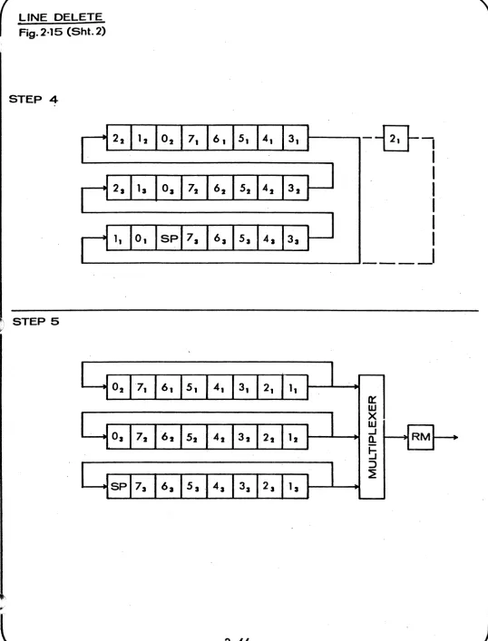
In order to understand the scroll operation in a little more detail, refer to Figure 2.7. Figure
(a) represents the three memory modules of 8 lines each. Just before the scroll ooperation (SCROL* goes low) the memories are tied together as one shift register of length 1920 characters. SPACE code is inserted in the last line (Line 7) of the bottom memory while the first line (Line 0) of the top memory is lost.
Returning to Figure 2.7, the registers are shifted for 80 counts in the long configuration. After 80 shifts SCROL* returns true and the memories are re-turned to their normal configuration as shown in Figure (b). Note that if during scroll operation the Tracking Counter (on Vidgen card) was allowed to shift then the SPACE code, instead of being
inserted in the last line of the bottom memory would appear in line zero of that memory. The same would be true of the other two memories.
In order to correct this the Tracking Counter is disabled during scrolling. This is done on the VIDGEN card.
In general, if the SCROLL operation occurs any time but when the Tracking Counter is at count 0, SPACE code would be inserted in the wrong line and by the same token the wrong line would be lost. Elaborating a little more, note that the SCROLL operation should not be enabled until the Tracking Counter reaches a character count of zero, otherwise part of the lines will get mixed up. From this i t is easy to appreciate the importance of having both the character and the ..
line count of the Tracking Counter at zero before
the information is shifted during scrolling.
In practice, this is achieved as shown in Section C-2. When the right conditions are met for scrolling CS, 10 goes true and sets up F/F BS, 9. (Note that scrolling is prevented during screen erase.) ADDCOM going true indicates that the character sitting on the cursor (assumed to be in line 7 of bottom memory)
is at the output of memory 3. This assures us that the Tracking Counter is somewhere on line 7 of the third memory. ADDCOM and the clock PHIB is, there-fore, used to set up F/F B6, 5. To make sure that the Tracking Counter has crossed the end of the last
line MCLEN* (Memory Clock Enable Not) is then used
to set up F/F B6, 8. This causes SCROL* to go false and initiates,the shift operation on the Memory Card.
SCROLLING OPERATION Fig.2·7
SPACE
• (a)
JUST AFTER SCROLL
y ,
I
H
I
G
I
F
j
E I
0I C·I
Bi=J
y
QI
p1
0I
NjM I L I
KI
Ji=J
Yspi
XIW I
Vi
u I
TiS
I
R~
(b)
Y
,lHIGIFiEIOlcl
B~
y
QI
pI
0I
Ni
MIL I
KIJ
i=J
Yspi
XIW
I
Vi
u
I
T i SI
R~
(c)
I
7I
6I
5I
4I
3I
2I
11
01
LOST
MEMORV 1
MEMORV2
MEMOR¥ 3
TRACKING COUNTER REF
TRACKING COUNTER REF IF ALLOWED TO SHIFT DURING SCROLLING
2.3.2.4
CR code on A6, 12 is used to cause prompt scrolling. This helps to speed up the scrolling operation nec-essary at high baud rates.
Cursor Control Logic
The cursor control logic [Section C-6, 7, 8] handles all the cursor movements, i.e., up, down, backward, forward and home position. One way to initiate these movements is by enabling anyone of the 5
cursor function keys on the keyboard [Section C & D-8]. These signal levels (as their names imply) are convert-ed to a strobe callconvert-ed FKYST (Function Key Strobe)
by the F/F E4 [Section C-7]. Depressing the REPEAT key on the keyboard will generate a repetitive FKYST with a frequency of 30 Hz. FKYST is generated by the rising edge of control functions. It is then ANDED with the control functions to generate the respective cursor control strobes. [Section B & C-6]. These are used on the VIDGEN card to update the Address Register and ADDCOM.
CURFR* (Cursor Forwar~ Not) goes low either for CURFOR (From the Keyboard) or for anyone of the following four signals:
PFCLK* DLACH* TABCL* HADRC*
(Protected Field Clock) (Data Latch)
(Tab Clock)
(Horizontal Address Clock)
PFCLK runs at the speed of PH2B (l.6MHz) whenever the cursor is in a protected field, i.e., whenever ADDCOM and TAGM and FON are true.
DLACH* pulses low whenever a character has been entered into the memory.
TABCL* is generated by the horizontal tab circuit [Section A-5]. This circuit helps to place the cursor in specific character positions (e.g., multiples of 5) at a rate faster than possible if done manually. This helps to speed up data entry. On receipt of HT code (Horizontal tab), F/F D4, 5
is set on the trailing edge of its input strobe. This enables the NAND gate C6 causing TABCL* to run at the speed of PH2B whenever ADDCOM is true. The cursor continues to move forward t i l l theF/F is reset by the signal TAB (goes true for character positions that are multiples of 5) when in Format OFF mode. If in Format ON mode the F/F is reset whenever the cursor goes through the entire page.
If during tabbing the cursor happens to enter a protected field, F/F 04 is promptly reset and the cursor is moved forward by PFCLK* to the first non protected position following the protected field.
HADRC* is generated by the Horizontal Address
Cir-cuit [Section A & B-3, 4, 5). As its name implies,
this circuit allows one to address the cursor in the horizontal direction upto a maximum of 166
posi-tions. The special sequence needed to initiate the
HADRC* is ESC, ENQ, X, Y, where X is the tens
digit in decimal and Y is the unit digit in binary. For instance, to place the cursor in the 78th
posi-tion, the sequence is ESC ENO 7 8.
ESC ENO cause B3, 3 to pulse high and the trailing
edge of INST sets the F/F B4, 9. At the same time,
BSYl* (Busy 1) goes low. When 7 is depressed LOY*
(Load Y) goes false and the code for 7 presets the up/down decode counter J5.to count 7. At the same time, the trailing edge of INST associated with 7
sets up F/F B4, 5 while BSYl* is held low. Next
when 8 is depressed F6, 8 strobes low and the code for 8 presets the counter J4 to a count of 8.
During both characters 7 and 8 BSYl* was held low
and hence INSD was disabled. This prevents 7 and
8 from being loaded into the memory. When 8 is
depressed B4, 6 goes true again and this sets up
F/F B2, 9 [Section A-4). The next PH2 sets up F/F
B2, 5 and allows CLKD* and HADRC* to run. Counters
J4 and J5 start to count down from the count of 78. HADRC* likewise runs at the speed of PH2B causing
the cursor to move forward. When the counters are
cleared to zero STP* (Stop) resets the F/F B2 and
thus disables CLKD* and HADRC*. The cursor is now
in the 78th character position.
Signals CURBK and CURUP [Section B-6) are
self-explanatory. When HOME key is depressed signal
HOME* is generated. This caus~s the cursor to go
to the start of page (in Mess. and Page Modes) since the signals CHRZ* (Character Zero) and LNZR* (Line
Zero) [Section F-3) go false. However, in CONV
mode HOME is at the beginning of the last line. To achieve this we first make the cursor go home as if
the system were in Mess. mode. The trailing edge
of the HOME function strobe is then used to' set up the F/F C2 [Section B-6) and after a delay of one
clock ti~e CURP is generated which kicks the
2.3.2.5 Character Generation
Character generation on the.980 Is obtained by ,
using the horizontal scanning technique. A
5 x 7 dot matrix is used to generate all
display-able characters. [Refer Figure 2.8] •• , The
charact-er field is an 8 dot wide by 9 scan line high "window". The character is generated' within this field in dot positions 2 through 6 and scan lines
1 through 7. Characters Rand S are shown in the
Figure 2.8 (a) to illustrate the point.
I t can be seen from the above figure that each character is generated from seven slices each
of maximum 5-dot length. Each time a scan line
is swept across, a 5-dot portion of the character
is generated.
The data line consists of 81 such windows. 80 of
these are used to display characters. The remain~
ing 1 is used at the beginning ' and at the end (1/2" at each end) of the line to form a margin for the white 'page.
The seven 5-dot patterns that make up a single character are pre-coded and stored in a cell in a Read Only Memory (ROM). Ll, L2 and L3 [Section
B, C, 0-1] form a bank of 3 ROMS. Each of the ROMS has a total capacity to store 64 characters, i.e., i t has 64 cells each of which can accomrnoda'te seven 5-dot patterns. Ll is called the Upper Case ROM
since i t stores 64 upper case characters.
Like-wise L2 is the Lower Case ROM.. L3 is.a special ROM. offered as an Option (64 character set). Ll and L2
together store the 128 character set on the ASCII CHART.
To obtain the 5-dot slice from the ROM, we have to
go through two levels of addressing. In the first
step, we have to address the cell where the
parti-cular character is located. In the second step, we
have to address the correct 5-dot slice. I t is easy to see that for proper character generation, the seven slices must be accessed in the right sequence. Each of the 64 cells is associated with a 6-bit
address (0-63). This address is chosen the same as
the ASCII code for the character. Refresh bits Rl
through R6G [Section G. B-2] are used as address bits. For example, the ASCII code for an R is 010010. This indicates that cell #18 contains the seven 5-dot pat-terns that make up the character R.
CHARACTER GENERATION Fig. 2·
a
SCAN LINES
r
1 CHAR4'CLK
01
Ia...._---'
DOT
04
J I "
I--_ _ _ _I I
_____ I
(a)
SRLO*=
51.--,
I
11---.
U..---D4*CLK
U
t
(b)LOAD R INTO ~3
-SCAN LINE· 1
·1
I
I
.1
•
•
tI
I
2
I
I
I II
I
3
•
I I I1
I
I
I
•
I
I
1
4
5
I I I
I
"1"
I I
I
6
7
I
2.3.2.6
Each of these seven patterns is then addressed
by 3 bits (0-7). The 'scan line counter Sl, S2, 54 are used to'address'the correct word within the cell. For example, the third 5-dot word of R is 10001 and is addressed by Sl
=
1, S2=
1,S4 ~ 0 which is the state of the Scan Line Counter during the 3rd scan line. These 5-dot patterns are then available in parallel at the output of the RYMS.
BecaUSe of the nature of horizontal scanning technique, the 5-dot parallel output has to be first converted into a serial form before being applied to the video mixer. This conversion is done by J3 [Section A-I). I t is an 8-bit parallel-in-serial-out shift register. Of these only 5-bits are used the others being tied to +5 Volts. Refer to Figure 2.8 (b) for timing diagram. Note that ample time is provided for the 5-bit pattern to become stable on the output lines before being loaded 'into the shift register. SRLD* (Shift Register Load) is decoded on the Vidgen card, and electrically it is a logical AND function of SRSTR
(Shift Register Strobe) [Section G-4) and DATA GT (Data Gate). SER (Serial) represents the serial output obtained from the shift register. I t is then mixed on the Vidgen card and applied to the video amplifier. Figure 2.8 (c) shows the seven serial slices of the character R one for each scan line.
Miscellaneous
The Master Oscillator for the video is in [Section
H-4 & 5). It is a crystal Oscillator consisting of
The signal, CLK, drives the first stage of the timing chain J7 [Section E-4] J7 is a SN74175 used as a Ring Counter. This causes the register to sequentially fill with ones and then with zeros. An entire period takes eight clock pulses. E3 is used to insure that no illegal state, such as 1010 may exist for more than one period. All
intra-character timing is derived from this counter which is also called the DOT counter. D4* (1.566 MHz or 639 n.sec.) represents one character time and drives the rest of the timing chain on the VIDGEN card. The last thing on this card is the Read Trigger circuit [Section B-7 &
B].
This circuit provides READT* (Read Trigger*) which sets the READ F/F on the ASYNC/FE card. F/F D4 can be reset either by depressing XMIT key on the keyboard, or when the terminal receives the commands DCl or SLOC (StartLocal Print). I t is set again by RTRST* (Read Trigger Reset*). Note that READT* cannot pulse low in CONV mode. Hence, no information ·can be read out of .
the memory in CONV mode.
Finally, the discrete components around the ROMS [Section F, G, H-2] are needed to supply the proper levels to the ROMS. Input levels must be 'between ground and +13V. The output drives must be sinked to a negative voltage and caught at +5V by the diodes D2-06 [Section C-l] to operate properly with TTL circuits.
2.3.3 Memory - Schematic #135-091..
The Mennory Section of the 9S0 is made 'up of two parts"-the Di~lay Memory and the Refresh Memory.
2.3.3.1 Dis:p1ay Memory
The Display Memory [Section A, B, C, 0-3] organization is ~odu1ar in nature. It consists of a group of shift re~sters running in parallel and recirculating their corrtents from the output back to the input. A single bitw of the 7-bits that form a character, is composed of a l28-bit static register in series with a 5l2-bit dynamic shift register 640-bits long. There are 7
such 640-bit long shift registers. In addition to thLs, there is another bit appended to characters. ThLs bit is called the tag-bit, and i t also has a 640-bit long shift register associated with it. This bank of 8 640-bit long shift registers form one module. I t has a total storage capacity of 5120 bits (8x640) or 640 8-bit long characters.. Since each line accommo-dates 80 characters, 8 such lines can be stored in a single memory module. Three such modules cover the entire screen of 24 lines or 1920 characters. Since the 3 modules are identical only one of them will be described in detail.
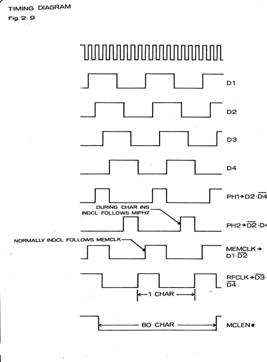
Shift registers K6, H6, L7, K7, J7, H7 [Section C, 0-3] make up one module. K6 and H6 are quad 128-bit static shift registers and L7, K7, J7 and H7 are dual 5l2-bit dynamic shift registers. The contents of these regist-ers are shifted at a rate of 1.566 MHz or 639 nanosec. which is one character time. The clocks MEMCLl, M1PHI and MlPH2 are AND functions of MCLEN* (Memory Clock Enable*) and PHI and Ph2 (Refer Timing Diagram for clarity) [Figure 2.9
J.
L6 and J6 are quad buffers whose function will be explained shortly. The outputs of L6 and J6 are returned again to the input of the registers via the multiplexers L5, K5, J5 and H5. This enables us to recirculate the contents and run in parallel. Hence at any time an entire character appears at the output of the shift registers. The 4:1 multiplexers (only 3 inputs are used) allow us to enter data into the memory or to ~crolt data. Depending on the states of the address lines of the multiplexer (pins 2 & 14) one of the three inputs is enabled. Normally both the lines are low. Thisenables input pin 6 and hence the memory contents are recirculated. However, when a character has to be entered into the memory, Al [Section D-4] momentarily goes true. This state of the address lines allows the output to follow input pin 5. Hence for one character time the recirculation path is broken and the character of interest is inserted into the memory. Still another manipulation of the memory occurs during the Scroll operation.
TIMING DIAGRAM
Fig. 2· 9
.J
~
I
I
r
DURING CHAR INS
'NOCL FOLLOWS M'PHZ ~ r--1
.
r--l~
___
~
______
~
I
~.
____ __
01
02
03
04
PH1+02'04
PH2+D2·04
NORMAlLY ,NoeL FOLLOWS MEMCLK~