Int. J. Electrochem. Sci., 7 (2012) 11876 - 11883
International Journal of
ELECTROCHEMICAL
SCIENCE
www.electrochemsci.org
Structural and Optical Properties of Zinc Oxide Film Prepared
Using RF-Sputtering Technique for Glugose Biosensor
A. J. Hashim1,*, Alaa J. Ghazai2, M. S. Jaafar1, NurAzimah Mansor3, ZainiharyatiMohd Zain3 1
School of Physics, UniversitiSains Malaysia 11800 Pulau Pinang, Malaysia. 2
Physics Department, Science College, Thi Qar University, Iraq 3
Faculty of Applied Sciences, UniversitiTeknologi MARA 40450 Shah Alam Selangor, Malaysia. *E-mail: [email protected]
Received: 4 September 2012 / Accepted: 15 November 2012 / Published: 1 December 2012
A zinc oxide (ZnO) thin film is fabricated on Si (110) substrate using the radio frequency sputtering technique. The good structural properties of the ZnO thin film on the Si substrate was confirmed via high resolution X-ray diffraction (HRXRD) and by scanning electron microscopy. The photoluminescence (PL) emission study included the optical properties of the ZnO film, and two PL peaks at 371 and 530 nm UV and visible regions were observed. A high oxidation current of 24.6 μM + 1.33 μA was applied at n = 5 of 10 mM H2O on sputtering Si-ZnO at a 0.05V/s scan rate. Glucose oxidase was then immobilized on the ZnO/Si electrode as glucose biosensor, with a limit of detection of 3.33 μM + 1.11 μM (n = 3). Finally, the response current increased linearly with glucose concentration in the range of 500 μM to 2100 μM with a correlation coefficient of 0.998 and a slope of 50 μA μM -1
Keywords: ZnO, RF-Sputtering, glucose biosensor, Amperometry
1. INTRODUCTION
Zinc oxide (ZnO) is an important material in many optoelectronic devices with wide applications such as varistors, biosensors, gas sensors, transparent electrodes, etc. [1]. ZnO is a promising material due to the wide direct band gap of 3.37 eV at room temperature (RT) and high exciton binding energy of 60 meV which allow it to use in ultraviolet region with harsh condition [2].
be monitored, i.e. the sensor without significant advances in control and instrumentation will not be possible [3].
Various techniques have been employed to prepare ZnO films including the sol-gel process, chemical deposition, direct current (DC) and radio frequency (RF) sputtering, and pulsed laser deposition [4]. The RF sputtering technique has drawn considerable attention since the resulting films properties can be controlled by changing the sputtering condition [3]
In this work the development of sputtered zinc oxide thin film was reported which has been deposited using RF magnetron sputtering technique on silicon Si ( n type) (110) , metallic zinc target has purity (99.98 % ) was employed. The films thickness of 950 nm is deposited at room temperature under high pressure (please state the pressure used) which has a significant role in the sensing applications.
A biosensor is an analytical device which consists of a biological material and a suitable transducer. Usually, the biological element is a tissue, microorganisms, enzymes, antibody, and etc. The transducer will transform the signal from the interaction of analyte with that biological element into electrical signal that can be more easily measured and quantified. Glucose biosensor is widely being used for diabetes incidences in consistent with drastic increment of diabetic cases in the developing countries. [5]. Glucose oxidase is immobilized on ZnO/Si electrode reacts with glucose producing H2O2. Anelectroactive species is oxidized by the electrode at a fix applied potential. The resulting current is proportionate to glucose concentration is measured.
region and high conductivity) as well as their process capability based conventional solution processes. [10].
2. MATERIALS AND METHODS 2.1 Fabrication of ZnO film on Si substrate
Firstl, the Si substrate was cleaned thoroughly using the RCA method. A thin film of ZnO was deposited on Si substrate using RF sputtering technique and its thickness was measured by using optical reflectometry system Filmetric F20-VIS. The crystalline structure of the film was studied using highresolution X-ray diffraction (HRXRD) Model; PANalyticalX’pert Pro MRD with a Cu-K1 radiation source of = 1.5406 Å. The microstructure of the film was studied by imaging the morphology of the film surface using scanning electron microscopy (SEM) and atomic force microscopy (AFM), while the photoluminescence spectra (PL) were recorded using photoluminescence spectroscopy system Model: JobinYvon HR 800 UV with He-Cd laser of 325 nm excitation source.
2.2 Fabrication and characterization of ZnO/Si glucose biosensor
Glucose oxidase (EC 232-601-0, Sigma Aldrich) was immobilized on the ZnO/Si surface. The ZnO/Si electrode is allowed to settle in 20 mL phosphate buffer saline (PBS) at a constant potential. Amperometric glucose calibration were carried out by standard addition known concentration of analyte in quiescent N2 saturated PBS using AutoLab Model PGSTAT302N. Calibration plot of averaged current density against glucose concentration was then obtained.
3. RESULTS AND DISCUSSION
3.1 Characterization of ZnO on Si substrate.
Figure 1 shows the XRD pattern of the deposited ZnO thin film on Si substrate which is confirmed the formation of crystalline ZnO. The XRD spectrum of ZnO film show mainly the ZnO (002) diffraction peak at 2 = 34.36°
Figure1. The XRD pattern of ZnO thin film on silicon substrate
The grain size along the c-axis was calculated to attain the detailed structure according to the Scherrer formula:
cos
9
.
0
B
D
(1)where λ is the X-ray wavelength, θ is Bragg angle of (002) peak, and B is FWHM value.
A large grain size of ZnO thin film of 9.81 nm on Si substrate was calculated, indicating that the grain become more uniform and bigger in size on the sample signifying an important role in reducing the defect inside the znO thin film.
In addition, The average uniform strain ezz for the lattice along the c-axis in the randomly oriented ZnO film deposited on Si substrate has been estimated from the lattice parameters using the following equation.
% 100
o o z
z
c c c
(2)
whereco is the lattice constant for the unstrained ZnO. The numerical value of c is calculated from XRD data according to the following equations:
sin
wheredhkl is the lattice spacing of (hkl), is the X-Ray wavelength and θ is Bragg angle. At the same time, ZnO is a hexagonal structure which follows the formula[11]:
2 2 2 2 2
/ /
) (
3 / 4
1
c l a k hk h dhkl
(4)
wherea and c are the lattice constants. The calculated c of ZnO thin film is 0.5215 nm, using co for ZnO of 0.52 nm [6]. The strain is equal to - 0.20 % for the ZnO thin film deposited on Si substrate. Negative value of the strain in the film means that the sample is in a compressive condition.
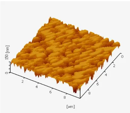
[image:5.596.183.411.327.495.2]We investigated the surface morphology of deposited ZnO thin film onto Si substrate using SEM and AFM. The SEM image of ZnO film is shown in Fig.2 which indicated that the deposited ZnO thin film on Si substrate has rough surface morphology and relatively big particles which are well connected to each other.
Figure 2. The SEM image of ZnO thin film on Si substrate
[image:5.596.190.405.559.747.2]
Fig.3 shows the film surface examined by AFM which reveal that ZnO thin film consist of some columnar structure grains. The grain height was found to be 100 nm with RMS 37.00 nm for ZnO thin film. This indicates that the surface roughness of the film on Si is high which is in line with the SEM resultobtained.
However, the smooth surface morphology of the film surface may be useful in the absorption of the UV light when it is used as a UV detector.
[image:6.596.132.447.242.479.2]The PL spectrum of the prepared ZnO thin film on Si is shown in Fig. 4. Two luminescence peaks can be observed in the sample, the first peak is the UV emission corresponding to the near
Figure 4. PL peaks of ZnO thin film on Si substrate
band edge emission (NBE) due to the electronic transition from near conduction band to valence band. The other one is in the visible region, which may be due to the defect, related deep level emission. The UV emission peak was found to be at 371.0 nm for the sample. Second luminescence peak, shows a broadgreen-yellow band peaked at 530.0 nm was observed for the sample.The Eg also could be derived from the PL spectra. The value was found to be 3.35eV for ZnO on Si. This result is slightly close to the bulk ZnOEg which equal to 3.37 eV.
3.2 Characterization of ZnO/Si glucose biosensor
[image:7.596.136.463.161.406.2]
transfer between the glucose oxidase and the electrode was achieved; thus the biosensor showed a low detection limit (3.33 μM + 1.11 μM, n = 3) obtained from the signal-to-noise characteristics of these data. Figure 5 illustrates that the response current increases linearly with glucose concentration in the range of 500 μM to 2100 μM with a correlation coefficient of 0.998 and a slope of 50 μA μM−1.
Figure 5. Calibration curve for glucose determination on Si-ZnO electrode.
4. CONCLUSIONS
A high quality ZnO thin film on Si substrate was fabricated in this study. Low grain size and smooth surface was observed in the ZnO sample. The ZnO film exhibited two high intensity PL peaks in the UV region at 371 nm, signifying its promising in UV optoelectronic devices. A good sensitive ZnO glucose biosensor using RF sputtering was achieved in which the response current increases linearly with the glucose concentration in the range of 500 μM to 2100 μM with a correlation coefficient of 0.998 and a slope of 50 μA μM−1. In summary,the high quality ZnO film on Si substrate was fabricated. The low grain size and smoothly surface observed in the ZnO sample. ZnO film has two PL peaks with high intensity in UV region at 371 nm make it promising to use in UV optoelectronic devices.
ACKNOWLEDGEMENT
References
1. M. willander ,O.Nur , Q. Zhao, L. Yang , M.Lorenz, B. Cao , J. Prerz, C. Czekalla, G.
Zimmermann , M. Grundmann , A. Bakin, A. Berhrends, M. Suleiman , A. El-Shaer, A. Chemofor, B. Postels , A.Waag , N. Boo-Kos , A. Travios ,H. Kwack, J.Guinard and D. Le, Nanotechnology, 20 (2009 ) 332001.
2. X. Sun and H. Kwork, J. of Appl. Phys, 86 (1999) 408.
3. C. Ahn , Y. Kim , S. Kang , B. Kong , S. Mohanta , H. Cho , J. Kim and H. Lee, J. Mater. Sci,: Mater Electron, 19 (2008) 744.
4. M. Lorenz, H. Hochmuth, C. Grüner, H. Hilmer, A. Lajn, D. Spemann, M. Brandt, J. Zippel, R. Schmidt-Grund, H. Wenckstern and M. Grundmann, Laser Chemistry,Hindawi Publishing Corporation, (2011) 1-27.
5. M. Chu, K. Miyajima, D. Takahashi, T. Arakawa, K. Sano, S. Sawada and K. Mitsubayashi, Talanta, 83(2011) 960.
6. B. Zheng, S. Xie, L. Qian, H. Yuan, D. Xiao and M. Choi, Sensors and Actuators B: Chemical, 152(2011) 49.
7. A. Kumar, H. Cheng and S. Chen, Reactive and Functional Polymers, 69 (2009) 364.
8. T. Kong, Y. Chen, Y. Ye, K. Zhang, Z. Wang, and X. Wang, Sensors and Actuators B: Chemical, 138 (2009) 344.
9. X. Liu, Q. Hu, Q. Wu, W. Zhang, Z. Fang and Q. Xie, Colloids and Surfaces B: Biointerfaces, 74 (2009) 154.
10. D. Lee, W. Ki, I. Park, D. Yoon, S. Lee and C. Lee, Solar Energy Materials and Solar Cells, 95 (2011) 365.