This is a repository copy of The phase-switched screen .
White Rose Research Online URL for this paper:
http://eprints.whiterose.ac.uk/800/
Article:
Chambers, B. and Tennant, A. (2004) The phase-switched screen. IEEE Antennas and
Propagation Magazine, 46 (6). pp. 23-37. ISSN 1045-9243
https://doi.org/10.1109/MAP.2004.1396733
[email protected]
https://eprints.whiterose.ac.uk/
Reuse
Unless indicated otherwise, fulltext items are protected by copyright with all rights reserved. The copyright
exception in section 29 of the Copyright, Designs and Patents Act 1988 allows the making of a single copy
solely for the purpose of non-commercial research or private study within the limits of fair dealing. The
publisher or other rights-holder may allow further reproduction and re-use of this version - refer to the White
Rose Research Online record for this item. Where records identify the publisher as the copyright holder,
users can verify any specific terms of use on the publisher’s website.
Takedown
If you consider content in White Rose Research Online to be in breach of UK law, please notify us by
The Phase-Switched Screen
Barry Chambers and Alan Tennant
Department
of
Electronic and Electrical Engineering Universityof
SheffieldMappin Street, Sheffield, S1 3JD, UK
Phone: +44 114 222 5588; +44 114 222 5438; Fax: +44 114 222 5834;
E-mail: [email protected]; [email protected]
Abstract
Conventional
(passive) radar-absorbentmaterials
operate either by phasecancellation
or
by absorbing incident electromagnetic energy and convertingit
intoheat.
This paperexamines a new
type ofactive
“absorber,” called the phase- switchedscreen
(PSS). The PSS operates quite differently frompassive
absorbersin that it
exhibitsan
apparently lowvalue
of
reflectivity by redistributing the electromagnetic energy incident upon itover a
bandwidth that is wide enoughto ensure
that little reflected energyfalls
within the pass-band of the receiver. The discussion considers the basic temporal and spectral properties ofseveral
PSS topologies, and includes measured data on both planar and cylindrical PSS structures.Keywords: Electromagnetic scattering; modulation; radar cross-sections; electromagnetic scattering by absorbing media;
intelligent materials; intelligent structures
I.
Introduction
hroughout history, humans have made use of stealth and
T
deception, firstly as hunters and then as warriors. In modem warfare, these skills have become ever more important due to the widespread use of all-weather, long-range sensors such as radar. Even from the earliest days of large-scale deployment of opera- tional radar systems, such as the UK Chain-Home system in the late 1930s, effort has heen put into ways of negating the radar detection and tracking of a target. At that time, the importance of target shaping was not appreciated, and so attention was concen- trated on the possible use of radar-absorbent materials (RAM) to reduce a target’s radar cross section (RCS). The earliest known RAM was that developed in 1936 in the Netherlands, for use on antennas [I], but by the early 1940s, the basic principles of both resonant and lossy-layer RAM were widely known 121. By 1945,these had been developed into the well-known Salisbury screen
[3], and the Jaumann and Dallenbach absorbers [4]. For nearly 60 years, many RAM designs have remained basically the same as they were in the late 1940s. However, improvements in perform- ance have heen achieved through the incorporation of new materi- als such as femtes, structural absorbers, and frequency-selective surfaces, and the wide spread use of computer-aided design [5-71.
The latter is crucial for the realization of a low-RCS vehicle, since, in practice, RAM treatments need to form an integral part of the vehicle design, so that non-specular wave propagation and scat- tering phenomena can he taken fully into account. Although in practice most RAM treatments are not in the physical form of flat panels, these are widely used in the research and development of new types of RAM, since this simplifies initial modeling and free- space testing. Hence, much of the discussion in this paper will he devoted to flat-panel RAM geometries.
So far, we have only considered what might be termed conventional or passive RAM. Although widely used, it does have
some disadvantages in practice. For example, RAM is designed to
meet a particular specification with respect to frequency, band- width, and reflectivity level, etc. However, this specification is fixed at the time of manufacture, and so if during the lifetime of a RAM-covered platform the threat changes, then either the RAM
has to be replaced, or a degraded performance against the new threat accepted. Also, as a number of authors have shown, the laws of physics limit the overall performance of passive RAM with regard to the reflectivity that can be achieved over a given hand of frequencies for a given angle of incidence and polarization. Of particular interest is the lowest frequency at which a desired value of reflectivity can he achieved for a given electrical thickness of
RAM 181. One possible way of improving RAM might be to make it active, i.e., to incorporate some means of changing the electrical parameters of its constituent materials. This might be done by using volumetric change, through materials such as controllable conducting polymer composites [9] or photo-dielectrics [IO], or by using discrete devices, such as semiconductor diodes [11-15].
Given that the same laws of physics will apply to both passive and active RAM, how can the latter improve on the former? Assume that in a particular electrical state, an active
RAM
has identical characteristics to its passive counterpart. If the electrical state ofthe active RAM is now changed, this will result in a new electro- magnetic configuration, so its characteristics will also change and be different from those of the passive RAM. Hence, the active
RAM
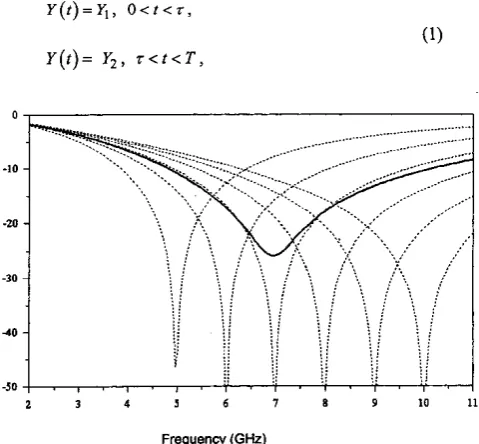
may have superior characteristics to its passive counterpad, when measured in terms of the sum of its instantaneous hand- widths. This argument must be used with caution, however, as the active RAM cannot by this means be used to synthesize the idealRAM, i.e., one having negligible reflectivity over all frequencies. To illustrate this, consider a simple active RAM structure, con- sisting of a Salisbuy screen in which the normal resistive layer has been replaced by one incorporating a parallel arrangement of fixed resistance and controllable capacitance. The predicted static reflectivity characteristics for a range of capacitance values are
shown as dotted curves in Figure 1. Hence, provided that the RAM has to deal with only one threat frequency at a time, then it can indeed be tuned to have optimum performance over a wide band of frequencies. If, however, there are many simultaneous and widely spaced threat frequencies, then it is the time-averaged RAM reflectivity that is important. The solid curve in Figure 1 shows the resulting time-averaged reflectivity when there are six threat fre- quencies, equally spaced over a bandwidth of 5 GHz. Now the RAM performance is degraded, since it can only dwell on each threat frequency for one-sixth of the time (assuming equal dwell times); furthermore, the time-averaged reflectivity at a given fre- quency is also degraded by the skirts of the reflectivity character- istics when the RAM is tuned to the other frequencies. In sum-
mary, active
RAM
can only he effective provided that its condi- tions of use are carefully defined. When deployed correctly, how- ever, active RAM may have additional functionality, such as being able to provide deception (e.g., instantaneous change from non- stealth to stealth mode, false Doppler), positive target identification (e.g., IFF: identification friend or foe), and smartness [16].2. The Modulating Surface
The concept of a modulating surface was first discussed in the late 1940s [17], but then and in its recent practical implemen- tations 118, 191 it was envisaged mainly as a means of covert communication. In this paper, however, we will discuss the appli- cation of a modulating surface to the problem of RCS control through its identity as an active “absorber.” Unlike the RAM ,(active or passive) discussed in Section 1, this new class of “absorber” does not actually absorb the incident electromagnetic energy, hut reflects it and at the same time redistributes it over a bandwidth that is so wide that little falls within the pass-hand of the radar receiver. Therefore, in its broadest sense the reflected signal resembles that produced by a spread-spectrum transmitter. The simplest method of doing this would he to utilize the Doppler effect. Several authors have considered the periodic Doppler shift produced at microwave frequencies by a flat PEC plate that is vibrated with a sinusoidal displacement in a direction perpendicu- lar to that of the incident wave vector [20, 211. In this case, the incident energy is redistributed on reflection between a component at the incident carrier frequency, f,, and an infinite numbel of sideband frequencies, which
are
determined by the plate vibration frequency, f,, and the maximum velocity attained by the plate during its sinusoidal motion. Because not all the reflected energy is now atf,
,
the vibrating surface appears to act as an “absorber” at this frequency, as measured by the receiver. Because of the obvi-ous
similarity to the process of angle modulation, the vibrating plate might be referred to asan
“angle-modulating surface.” To assess its usefulness in practice, consider the ideal case when all of the incident energy at f, is to be redistributed among the reflected sideband components, and all are to lie outside the pass-band, 2 8 , of the receiver. Following [21], the amplitude of the signal reflected from the plate at f, is proportional to J 0 ( 2 fcvm,/ f v c ) , where J,, is the Bessel function of the first kind of order zero, andc = 3 x 10⁸m/s. Then, since Jo (x) = 0 when x = 2.405
,
and let- tingf, = 10 GHz and f, = B = 5 MHz, the required value of vmais approximately 1.8x10⁵mis. This results in a maximum plate displacement of approximately i5.1mm. Clearly, these require- ments are impractical for a large-area mechanically actuated sys- tem, and so an altemative modulating structure must he sought.
One solution lies in requiring the plate to he positioned repetitively at one of only two positions in space, rather than at an infinite number. This may be synthesized electronically, thus eliminating limitations on performance due to the inertia and mass of the plate. Thus, the “phase-switched screen” (F‘SS) achieves an effect similar to the angle-modulating surface, but by applying binary phase-shift modulation to the incident signal. This has the advantage that the resulting reflected signal will have inherent cancellation of the component at f, [22].
Several approaches may he used to explore the properties of the PSS. The first of these is based on conventional spectral analy- sis, from which it is easy to comprehend the basic principle on which the PSS is based, and to investigate topics such as the opti- mum choice of PSS switching characteristics: this will be consid- ered in Section 4. For an investigation of the optimum choice of the switched sheet impedances and its inflnence on PSS band- width, however, a circuit description, based on a transmission-line analysis (TLA), is probably more useful, and will he considered in Section 3. This approach is valid for both CW and pulsed incident signals, since the duration of a radar pulse is very long compared with the wave transit time through the PSS structure, and com- pared to the time for one half-cycle of the switching waveform used to control the active layer(s) in the PSS.
3.
TLA
Analysis
of
the
Single-Active-Layer
PSS
‘The transmission-line analog o f a typical single-active-layer
PSS
is shown in Figure 2 . It consists of a short-circuited length, d , of transmission line, with characteristic admittance Y, andpropagation cnnsmt
0.
A time-varying admittance,Y
[ I ) , across is placed across the input terminals of the transmission line, whereY [ I j i s defined IO he
Y ( t ) = Y I , O < t < r ,
Y ( r ) = Y,, T < t < T ,
[image:3.614.324.564.439.661.2]Frequency ( G M )
Figure 1. The predicted time-averaged reflectivity (vertical axis, io dB) characteristics of active RAM over a wide band- w i d t h the dotted line is for a slow tuning rate; the solid line is for a fast tuning rate.
This leads to the general condition for the PSS, which relates
qnl
andqnZ
to5.
Thus, from Equations (3) and (4),(a) parallel polarization
( 5 ) I - - (Y -Y
)=-,
yo',:,(
f)
m2 ml cos2e
@) perpendicular polarization
qnl&2
+Yo cos0 1--( q n 2
-
qnl)
= Yo'cos' 8 . ( 6 )(
3
In tbe simplest case, when r = T / 2 , Equations ( 5 ) and (6) simplify to
.
,d
2
y y
-r,
cos2e
'ml ,n2 -
(7)
.
,
d
Figure 2. A short-circuited transmission line shunted by a time-varying conductance
where 7 is the "on" time and T i s the time period for one cycle of
the waveform used to control the state ofY(t). Depending on the incident polarization and angle of incidence, 6 ,
&
is given either by Ye = 0 for parallel polarization, or Y, = Yo cos 0 for perpen- dicular polarization. For either polarization, is given byp
=Po
cos 0 . Thus, the input admittance of the PSS can assume one of two states, eitherTn1
orTn2
,
given byY
case
qnl
=r;
-
j& cot pd,
q n z = Y 2 - j Y , c o t p d .
These result in reflection coefficients p, andp2, which are related to &,I and
qn2
by(3)
YO
where Y =- or Yo cos8 for parallel or perpendicular polariza- tion, respectively. Since and are arbitrary, then p, and
p2 are generally complex.
e
For the PSS to behave like a perfect absorber at a particular frequency, then the reflection coefficient, p , when averaged over time T, must he equal to zero, i.e.,
lEEE AntennasandPropagation Magazine, Vol. 46, No. 6 , December 2004 25
qn1q"2
= Yo' cos2e,
or when written in terms of the switched admittances,
5
and5 ,
(a) parallel polarization1
[r,
- j$c0t(/3~dcos8)A c o t ( p o d c o s B ) ] =
yo',
(8)[Y2-Jcos8 cosz
e
(b) perpendicular polarization
[YI - jYo cosOcot(~odcos8)]
[
Y2 - jYo cos 8 cot(
pod
cos 8)] =Yt
cos' 6'. (9)If the incident frequency,
f,,
is such that dcosO=-,4
then4 li
podcos 0 = - , and Equations (8) and (9) simplify to
2
yo2
qr,
=-cos2
e
'Since the time-averaged reflection coefficient, p , is zero, the PSS behaves like a perfect absorber at f,, as expected. When dcos8#-,
4
p will not, in general, he equal to zero, but will4
depend on the particular form of
4
and Y2 [23]. To simplify the discussion that follows, letr;
= G I ,&
= G2, and 0 = 0" (the oblique-incidence case is discussed in [24]). Then, Equations (IO)and (1 1) hotb simplify to
RlR2 = Z i
,
(12) [image:4.613.62.303.50.276.2]Frequency (GHz)
Figure 3. The frequency characteristics of a passive Salisbury screen (solid line) and of a single-layer planar phase-switched screen, d = 7.5 mm (dashed line). The vertical axis is the reflec- tivity in dB.
Equation (12) has been repotted previously in connection with diode-switched reflection phase shifiers [25], hut was derived independently for ‘active radar absorbers in [26]. Although not mentioned in the literature, Equation (12) also applies to the pas- sive Salisbury screen, since it relates the two possible values of front sheet resistance that give a particular reflectivity-null depth.
In principle, there is an infinite uumher of pairs of resistance values that will satisfy Equation (12). However, in the experimen- tal PSS to he described later, the switched resistive layer takes the form of a frequency-selective surface (FSS), consisting of
PZN-
diode-loaded dipole elements that are biased either fully “on” or fully “off.” Hence, to a reasonable approximation over the band- width of the FSS, RI=On
and R2=ma.
Then,+-I,
p2 --f +1, and the time-averaged value of p 0 as expected, since the “on” time, P = T / 2 . If the value of d is now fixed, it is easy to show that as ‘f varies, then p varies as cospd (and, hence,
reflectivity = 201ogl0(Icosfld(). Figure 3 compares this frequency
variation of reflectivity with that for a Salisbury screen with the same value of spacer thickness, d. It can he seen that the bandwidth of the PSS is somewhat narrower than that of the Salisbury screen, and this behavior may he explained by considering the influence of multiple reflections inside the PSS structure. When R1 and Rz
only take on values of 0 or m , the incident wave is only reflected from either the front or the back face of the PSS, and no multiple reflections can occur. However, for other combinations of R1 and R 2 , some of the energy incident on the front face of the PSS can always penetrate into ,its interior, thus giving rise to multiple reflections that will change the frequency characteristics. In the limiting case, when RI = Rz = Z , , then the frequency characteris- tics of the PSS become identical to those of the Salisbury screen.
From Figure3, it can he seen that at resonance (i.e.,
pod
= z / Z ) , the effect of switching R ( t ) between values RI and R2 ~ as related by Equation(12) ~ mimics the reflectivitycharacteristics of a passive layer having a sheet resistance equal to Z ,
.
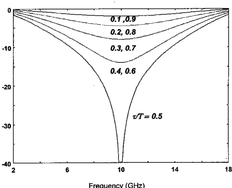
Hence, it should he possible to adjust the effective sheet resis-tance, R e f , by varying the “on” time,
r
,
in each switching cycle.The relationship between Ref and r is given by [26]
and the dependence of the resonance-null depth of the PSS on TIT is shown in Figure 4. Hence, the PSS may he configured to act as a reflector or as a variable absorber, simply by changing the mark-
space ratio of the control waveform applied to the switched resis- tance layer. This behavior is confirmed by the measured data shown in Figure 5 .
The normal single-layer PSS has a switchable front layer, A, and a PEC backplane. In some applications, where the. structure to he shielded from an incident wave is thin (e.g., a missile fin), it might he advantageous to replace the PEC backplane by a second switchable layer, B, thus giving rise to a bidirectional PSS (BPSS) that is effective against illumination from either side of the stmc- ture. In operation, each active layer is switched so that at succes- sive instants in time, RA = 0 , RB = m ; RA = m , R B = : O ; RA = 0 ,
RB = m
,
etc. From Figure 4, it can he seen that the bidirectional PSS will then have the same apparent reflectivity when viewed from either side.Although the transmission-line analysis of Section 3 enables us to examine the frequency characteristics of the PSS, it does not allow us to determine the optimum choice of switching-waveform shape and frequency, particularly in the presence of pulsed incident signals. This will he considered in Section 4.
4.
Spectral Analysis
of
the
Single-Active-Layer PSS
For simplicity, we will consider here only the case of a single-active-layer PSS, operating against a periodic train of rec- tangular pulses of carrier frequency
f,
[27], as shown in Fig--30.
-40
’
I2 6 i o 14 18
[image:5.613.68.307.45.222.2] [image:5.613.325.564.488.682.2]Frequency (GHz)
Figure 4. The variation of null depth with PIT for a resistively switched PSS. The vertical axis is the reflectivity in dB.
T
J
cn ='
Zn77
and
M
e-2(m-l)r + ce;2Bde-2W + e - ( Z M + l ) ~
m=l
1-q
277
[image:6.613.68.303.47.197.2]p = - .
a
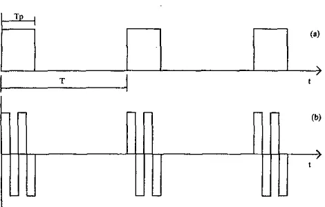
Figure 6. The operation of the phase-switched screen: (a) the incident wave; (b) the reflected wave ( M = 2 ; for clarity, the sinusoidal carrier-frequency signal itself is not shown).
ure 6a. Each pulse is of length Tp , and the pulse repetition period is T. After reflection from the PSS, assume that each incident car- rier pulse is replaced by
M
cycles of a bipolar rectangular wave- form, as shown in Figure 6b. Hence, the period of this modulating waveform, 2 r , is given byT
M
2 r = P , (14)
M
and the switching frequency, f, , is given by f, =
-
TP
Since the incident pulse train is periodic with period T, its spectrum and that of the signal reflected from the PSS may be determined using Fourier analysis. Hence, the incident and reflected signals may be written in the form
where 00 = 2771T. The complex Fourier coefficients, c, , are then given by
C" = q " ( t ) e - ; n % f . (16)
TO
For the incident periodic pulse train, the c, are given by
For the PSS-modulated wave and M an integer, cn may be written in the form
where
In the general case of non-integer
M,
Equation ( 1 8 ) is modified to(a) M = M + G M , O < S M < l / Z ,
0 < x
<
r , (23)(b) A4 = M + 6 M , 112 2 6 M 2 1 ,
ues of switching frequency, the predicted values of PSS reflectivity agree with those calculated from 20IoglO(lcos/3dl). The results shown in Figure 7 may be scaled so that they are applicable to other pulse widths and receiver bandwidths. For example, if the pulse width is decreased by a factor of IO, then the receiver band- width and the switching frequency must he increased by the same factor to give the same value of reflectivity as before.
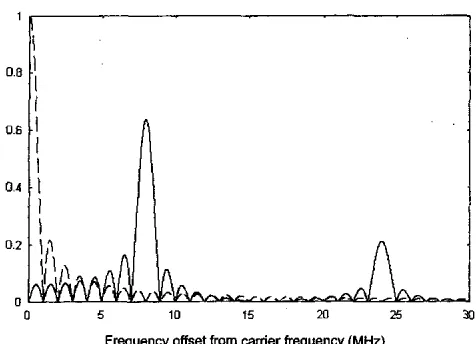
Consider now the spectrum of the PSS-modulated signal. Figure 8 compares the spechum of an incident signal, composed of a train of 1 psec pulses of carrier frequency 10 GHz and duty cycle of I%, with that of a signal reflected from a PSS the reflection coefficient of which is switched between f l using an 8 MHz bipo- lar square waveform. It can be seen that the level of the signal reflected at
f,
has been reduced considerably, and that the energy originally at f , has been redistributed mainly amongst the side- bands positioned at f, f 8 n MHz, n odd. Figure 9 shows the corre-I
I
_--,-.
.
--0 5 10 15 20 25 30
SwiWling frequency (MHz)
Aigure 7. The reflectivity (vertical axis, in dB) of a planar single-layer PSS with 1:l bipolar square-wave switching: 1 psec pulse length, 1% duty cycle, 2 MHz receiver bandwidth.
- f c - - I O G H z , - - - f , = l I G H z , - . ’ fC=15GHz.
l h 1
li
I
[image:7.613.321.556.53.225.2] [image:7.613.71.304.249.424.2] [image:7.613.69.307.488.660.2]Frequency oiiset from carder frequency (MHz)
Figure 8. The one-sided frequency spectrum of a pulsed carrier signal incident on and reflected from a PSS switched at 8 MAX
f, = IOGHz, 1 psec pulses, 1% pulse duty cycle; - - - incident signal, - reflected signal. The vertical axis is the normalized spectrum amplitude.
0 5 10 15 20 25 a
Frequency offset f” carrier frequency (MHz)
Figure 9. The one-sided frequency spectrum of a pulsed carrier signal incident on and reflected from a PSS switched at 8 MHZ:
f,
= 15 GHz, 1 psec pulses, 1% pulse duty cycle; - --
incident signal,-
reflected signal. The vertical axis is the normalized spectrum amplitude.sponding spectrum when the signal incident on the same PSS is at a frequency of 15 GHz. In this case, less energy is redisbibuted from around
f,
into the sidebands, and so the resulting apparent reflectivity performance is worse than that at 10 GHz. Experimen- tal confirmation of the spectral spreading provided by the PSS is shown in Figure IO. In this case, a single-active-layer PSS, opti- mized for use at 11 GHz and operating in free space, was iliumi- nated by a pulsed 11 GHz plane-wave signal (1 ps pulses with 0.1% duty cycle), and the PSS was. switched at 20 MHz. Hence, from Figure IO, a receiver with a 2 MHz bandwidth would “see” the PSS as exhibiting a reflectivity of less than -30 ds, which is in good agreement with the predictions for the I O Gllz optimized PSS when also switched at 20 MHz, as shown in Figure 7.Retuming now to Figure 8; if the PSS was being used to reduce the apparent radar cross section of an object, a possible countermeasure might be to use a wideband receiver to detect the reflected spectral components at
f,
f 8 MHz. An obvious method of avoiding this would be to increase the PSS switching frequency,f,
,
but if the PSS surface was electrically large andf,
was high enough, this might cause EMC problems or the PSS might even act as a beacon atf,
or its harmonics. Careful design and layout of the PSS surface should avoid these problems (see also Section 9.2), but here we look briefly at a solution involving spectrum-spreading techniques, whereby the 8 MHz sidebands are broadened out by switching the PSS reflection coefficient in a non-periodic m e r .Because such cases are not easily amenable to analytical solution using the previous Fourier-analysis technique, all the results to be discussed from now on were obtained numerically, using the FFT.,
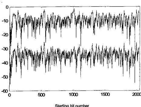
The sideband energy in the PSS-reflected signal may he spread out by changing the effective PSS switching frequency within the period of one radar, pulse. For example, the upper c y v e in Figure I 1 shows the effect of switching using a waveform that has been generated by choosing consecutive 16-bit strings (since the nominal switching frequency of 8 MHz is equivalent to 16 half-cycles within the 1 psec radar pulse) from the primitive poly- nomial (modulo 2) sequence, of order 11 [28]. The overall m
sequence is 2047 (2”
-
1 ) bits long, to which has been added an additional 0 bit, so as to equalize the number of Is and Os (to5~
Figure 5. The measured variation of the null depth for a resistively switched single-active-layer PSS.
-10 -
-
-15
[
- 2 0 ~-25 -
Jo
8 9 10 11 12
~ ~~
14
13
#4 Mkuf
1158:43
Mav 8.2883
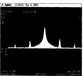
IFigure 10. The measured free-space frequency spectra of pulsed incident and PSS-reflected signals. The incident carrier frequency and PSS center freqnency were 11 GHz, the pulse length
was
1 psec, the duty cycle wasO.l%,
and thePSS
switching frequency was 20 MHz. The incident signal is in yellow, and the reflected signal is in
cyan.
Figure 24. The conhol of the null position and depth
in a two-active-layer PSS by varying the layer
“on”
times. The vertical ad8 is the reflectivity in
dB.
Frequency ( G W
0.7
a, - 0 -0.2 -0.4 -0.5
__
0.55-
Starting bit number
Figure 11. The variation in PSS reflectivity (vertical axis, in d e ) as the 16-hit switching sequence contained within the width of a 1 p e e radar pulse was chosen sequentially from an overall switching sequence of 2048 hits. The top curve shows bipolar switching based directly on the hit sequence generated by an 11th-order polynomial (modulo 2) (mean reflectivity value = -10.2dB). The bottom curve is the same as the top curve, hut when Manchester eneodiug was used (mean reflec- tivity value = -35.ldB).
ensure a zero dc level and, hence, zero reflected energy at f,). A M e r refinement is to then represent each 1 or 0 in the hit sequence using Manchester encoding. This breaks up local repeated occurrences of 1s or Os in the sequence, thus smoothing out the spectrum, as well as increasing the effective switching fre- quency to approximately 16 MHz. The benefits of including this
additional process may he seen by comparing the upper and lower c w e s shown in Figure 11.
Although in practice better switching strategies and higher switching frequencies would be used, it should he noted that the form of optimum spreading codes for use with a PSS might differ considerably from that of those used in spread-spectrum communi- cations. There are two reasons for this. Firstly, because it is highly undesirable for an unauthorized recipient of a PSS-modulated sig-
nal to he able to reconstruct the switching sequence and so
'"ask" a PSS-shielded object through appropriate signal proc- essing in the receiver, the autocorrelation properties of the PSS switching sequence must be designed to protect against this. Sec- ondly, it is highly desirable for the number of 1s and Os in those portions of the PSS switching sequence that are used while radar pulses are actually illuminating the PSS be equal or nearly so,
since this ensures good suppression of the incident carrier- frequency component, f c , by the PSS. For this reason, switching sequences generated using primitive polynomials alone are not suitable, because of their inherently poor localized distribution of 1s and Os. Herein lies the advantage of additional Manchester encoding, since this condition is then automatically fulfilled [27].
5. Reactive Single-Active-Layer
PSS
The discussion so far has considered a PSS with a single active layer that can he switched between two values of surface resistance, which are related by Equation (12). A limitation of this
30 IEEE Antennas andPropagatton Magaznre, Vol. 46, No. 6, December 2004
structure is that it can only provide a single reflectivity null with a limited bandwidth. However, the bandwidth can be increased sig- nificantly if the active layer is reactive. This approach is similar to that used in the design of passive-circuit analog absorbers, where a reactive impedance sheet is used to counteract the change in elec- trical-spacer thickness with frequency [6].
It can be shown that a PSS with a single active layer, which is switched between reactance values of ? jZo sin ,Bod by an equal- mark-space-ratio square wave, has zero time-averaged reflectivity over a frequency band defined by 0 <,Bod < li. For example, a
5 mm-thick air-spaced PSS could, theoretically, exhibit zero reflectivity from 0 to 30GHz. I n terms of a circuit analog, the active layer is switched between inductive and capacitive reactance states described by Z1 = j o L and Z 2 = 1/ jwC , Here, hoth L and C
are functions of frequency, as shown in Figure 12, and are such that they are resonant at all frequencies within the operating band, i.e., f = 1 / 2 a a , Although such a reactive layer is not physi- cally realizable using currently known materials, the use of reac- tive impedance switching can nevertheless significantly increase the bandwidth of a PSS, as shown by the measured data in Figure 5
and the following theoretical examples. The first case to he exam- incd is that in which the impedance layer is switched between two states that correspond to fixed values of inductance and capaci- tance, i.e., Zl = j o 4 and Z , = l / j u C , . Figure 13 shows the
reflectivity characteristics of a 5 mm-thick air-spaced PSS for which
4
= lOnH and Cl = 64.5 E. In this example, the values of capacitance and inductance have been chosen to optimize the -20 dB reflectivity bandwidth.
A closer approximation to the impedance states of the ideal active layer, Zl,2 = ? j Z o sin Pod , can be acbieved over a limited bandwidth by using a layer that contains both inductance and
804, I I I I I I I
I
Figure 12a. The Capacitance of a PSS active layer required to give zero reflectivity.
I I I ! I I I
1
2 4 6 8 I Q 12 14 16 I 8
0
Frequency (OHz)
[image:9.613.70.303.52.230.2] [image:9.613.320.553.434.538.2] [image:9.613.319.553.588.688.2]Figure 13. The predicted reflectivity characteristics of a switched-reactance single-layer PSS:
-
d = 5 mm, L1 = 10 nH, C,=64,5fF;- -
-d = 5 m m ,
L,=0.975nH, C,=72fF,&
= 94 nH, C2 = 5.7fF.
,
5”
i
1
diode loading--
‘v
.r
points
/
[image:10.613.63.299.50.189.2]dc
bias
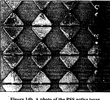
Figure 14a. The layout of the PSS active layer.
lEEE Antennasandpropagation Magazine, Vol. 46, No. 6, December 2004 31 Figure 14b. A photo of the PSS active layer.
h capacitance,
i.e., Zl =jmh
+ I / j d l and Z2 = j o L 2 +l/iWc,. Using this approach, the reflectivity bandwidth of the PSS consid- ered in the previous example can be increased to provide a response of at least -20 dB over more than one octave. A second design is also shown in Figure 13, for whichI,
=O.Y75nH,C, = 72
fF,
and4
= 94 nH, C, = 5.7 fF. This now raises the ques- tion as to how reactance can be incorporated into the active layer. In ow layers, reactance is always present by default, since the for- mer are based on switchable frequency-selective surfaces that are controlled by PIN diodes.6.
How
to Build a
PSS
To realize a practical PSS, we need a surface that can be rap- idly switched between two or more impedance states. Potentially this could be achieved using some type of functional material, such as an active conducting polymer [9], but to date we have concen- trated on the development of layers comprised of a two-dimen- sional grid of half-wavelength dipoles that are loaded at their cen- ters with PIN diodes. Under no-bias conditions, the PIN diodes present high microwave impedance, and the dipoles may be con- sidered open circuit. Hence, the grid of dipoles is nonresonant, and represents a high-impedance equivalent surface. When the diodes are biased “on,” however, their microwave impedance becomes low, and the dipoles are resonant at the half-wavelength frequency. Then, the grid of shorted dipoles becomes a strong scatterer, and represents a low-impedance surface. The basic geometq of the active layer in OUT PSSes is shown in Figure 14 [2Y]. The layer is based on a unit cell containing a howtie dipole, which is loaded at its center by a PIN diode contained in an SOD323 package. In order to connect adjacent diodes in series strings, each dipole has a short tab at one end, and this also serves to add a controlled amount of inductance to the circuit, so as to broaden its frequency response. Also shown in Figure 14 is a close-up view of part of an active layer containing 900 elements.
7. Dual-Polarized PSS
The practical PSS design discussed in Section 6 is only sensi- tive to a single linear incident polarization. In most operational situations, however, a dual-polarized PSS would be advantageous. In this section, we describe some of our initial work on the design
of a dual-polarized screen. An obvious approach to the design of a dual-polarized active layer would be to fabricate two linearly polarized dipole-grid arrays, arranged on opposite sides of a thin substrate. However, a problem with this approach is that although the substrate can be made very thin (10microns) - using, for example, a Mylar substrate ~ the surface-mount PIN diode pack-
ages that we currently use are approximately I mm high. This results in different effective electrical spacings between the back- plane and the two active layers. Hence, we are investigating an alternative topology, which combines two orthogonal grids of bowtie-dipole elements along with an integrated diode feed net- work that can be fabricated on a single-sided printed-circuit board, as shown in Figure 15 [30].
[image:10.613.74.291.258.707.2] [image:10.613.86.279.539.716.2].Figure 15. The details of the dual-polarized active-surface unit- cell geometry (all dimensions in mm), and a representation of the grid layout.
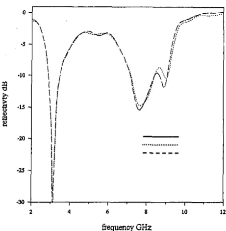
low-loss, foam dielectric spacer ( E , = 1.05, tan8 = 0.0017). Com- plex reflectivity data were measured for this loose-lay configura- tion over a frequency range of 2-12 GHz for linear incident polari- zation at rotation angles of 0", 45", and 90°, respectively. For each measurement, two data sets were recorded one with the lose-lay PSS containing the open-circuit FSS, and the other with the short- circuit FSS. The measured data were then used to synthesize the reflectivity performance of an active PSS modulated by a periodic square wave by combining the data using Equation (4), where p,
and pz represent the complex reflection coefficients of the PSS measured with the open-circuit and short-circuit FSSes, respec- tively. The synthesized reflectivity response of the PSS at polari- zation angles of O", 45', and 90" are presented in Figure 16. The bandwidth response
of
this prototype dual-polarized design is compared to that of the linear screens, and we are curently work- ing on new FSS topologies to provide a wideband response.8.
Conformal
PSS
In many practical situations where RCS (radar cross section) control is an issue, the object under consideration will not be pla- nar, and any coating, or screening structure, will need to conform to the geometry of the object. As a first step towards this problem, we
now
briefly examine the application of PSS techniques to cylindrical surfaces. A theoretical description of some of the design issues relating to a cylindrical PSS may he found in previ- ously published work [31, 321, so here we restrict the discussion to a report of our experimental work.As in the planar PSS designs, the active surface has been formed &om a periodic grid of PIN-diode-loaded bowtie dipoles. However, to allow closer packing of the elements on the grid (nec- essary because of the small radius of the particular PSS design pre- sented here), the flare angle of the bowtie dipole was reduced. To allow the formation the cylindrical PSS geometry, the active sur- face was fabricated on a flexible Mylar substrate. An experimental cylindrical PSS was formed, using a 120 mn-long, 16 mm-radius aluminum bar as "the backplane." The dielectric spacer consisted of a Perspex tube ( E , = 2.6), with inner and outer radii of 16 mm
frequency GHz
Figure 16% The reflectivity iesponse of the dual-polarized active
PSS,
synthesized from measured data ( r = 0.42).2 I 6 8 10 12
eequency GHt
Figure 16h. The reflectivity response of the dual-polarized active PSS, synthesized from measured data ( r = 0.54).
[image:11.614.323.554.180.416.2] [image:11.614.323.555.464.696.2]I
a
-20+-
I
.?"
I-"-
-35
8 9 10 11 12 13 14 15
[image:12.616.68.300.51.221.2] [image:12.616.69.302.269.439.2]h q u s n c y w 2
Figure 17. The measured reflectivity response of the cylindrical
PSS.
I
\
i
i
/I
2 b 6 8 10 I t 14 16 18
Frequency (GHz)
Figure 18. The reflectivity (vertical axis, in dB) characteristics of a skinned (solid) and an un-skinned (dashed) single-active- layer PSS. The thickness of the sliiuued PSS was 8.7 mm; the thickness of the un-skinned
PSS
was 6.25 mm.and 21 mm, respectively, providing an electrical spacer thickness of approximately 8.0 mm. The complete PSS structure was formed by wapping the flexible active surface around the spacer, with the surface-mount PIN diodes facing outwards. As the active surface was designed for linear polarization only, two configurations were used to test both TE and TM illumination. For the TM PSS, the bowtie dipoles of the active surface were arranged parallel to the cylinder axis. For TM illumination, the dipoles were perpendicular to the cylinder axis.
Figure 17 shows the measured reflectivity responses of the TE and TM PSSes (these c w e s are referenced with respect to the bare aluminum cylindrical backplane). In both cases, a reflectivity null of less than -2OdB was achieved over bandwidth greater than
1 GHz. The null response of the TE PSS occurred at a higher fre- quency than that of the corresponding TM PSS, and this result is consistent with the theoretical predictions presented in [29, 301 for a cylindrical PSS of relatively small radius. However, the differ- ences may also in part be due to the different impedances pre- sented by the TE- and TM-configured active layers, but this has yet to be investigated.
9. Other Types
of
Single-Active-Layer PSS
9.1 Skinned PSS
A well-known technique for improving the bandwidth of the Salisbury screen is to place a thin, high-permittivity skin in front of the resistive layer [33]. The skin not only introduces additional multiple reflections within the absorber shucture, but it also pro- tects the resistive layer from mechanical or environmental damage. The same technique can also be used with the PSS, and Figure 18
compares the predicted reflectivity performances of a skinned and an un-skinned single-active-layer PSS. It can be seen that the pres- ence of the skin is very beneficial in terms of increased bandwidth, for only a modest increase in thickness.
9.2 Double Diode Switching Elements
I€€€ Mtennasandpropagation Magazine, Vol. 46, No. 6, December 2004 33 Earlier, we discussed how the signal reflected from a single- active-layer PSS could be spread using appropriate pseudo-random binary switching sequences. Here, however, we consider an exten- sion to the technique that uses only a simple periodic switching voltage. If the frequency of the latter is made very high, so as to move the first sideband frequencies well away from the incident camer frequency, then problems may arise when the surface area of the PSS is electrically large. These are due to propagation effects in the PIN-diode-biasing network, and the fact that the PSS may start to radiate at the switching frequency or its harmonics. Hence, what is required is a technique for achieving the beneficial effects of a high switching frequency without the associated penal- ties. One promising solution is to replace the single PIN diode at the center of each dipole in the PSS active layer by two diodes, arranged as an anti-parallel pair [34]. This arrangement of diodes was first suggested in [35] for use as a millimeter-wave harmonic mixer, in which the local oscillator signal is supplied as a sub-mul- tiple (typically, one-half) of the wanted frequency. In the case of
the PSS, the voltage stimulus waveform takes the place of the local oscillator signal, but the net effect is the same. The spectrum of the signal scattered from the modified PSS should contain only side- band components at even harmonics of the switching frequency. Hence, the double-diode P S S performs as though the switching frequency has been doubled, as compared to that of the single- diode case. It should be noted that for this arrangement to operate correctly, the voltage stimulus applied to the PIN diodes in the PSS active layer now takes the form of a bipolar sine wave, rather than the square wave used previously. As an illustration of this tech- nique, Figures 19 and 20 show the measured free-space spectrum of a signal reflected from a large-area P S S panel, operating at
10.44 GHz, the dipoles of which are center-loaded by an anti- parallel diode pair contained in a single SOD323 package.
Figure 19 shows the effect of operating the new PSS.under non-optimum conditions. Even though the sine-wave voltage stimulus is adjusted correctly and frequency doubling of the switching frequency is evident in the reflected spectrum, the latter still contains a large-amplitude component at the incident carrier frequency. This may be explained by considering the time:aver- aged reflectivity of a finite-area single-layer PSS, pa,,, to he,com: posed of two components associated with the ON and OFF states.
Figure 19. The spectrum of the signal reflected from a PSS with two diodes per array element. SoFP and SON were not
balanced, the switching frequency was 5 MHz, and the vertical scale is 10 dB/div.
Figure 20. The Spectrum of the signal reflected from a PSS with two diodes per array element. SoFF and So, were hal- anced, the switching frequency was 5 MHa, and the vertical scale is 10 dB/div.
hence, pa” = poNsON +pOFFsoFF
.
Then, even if poN = -poFF,2
pa” will not be equal to zero if So, f SoFF. In the PSS contain- ing one diode per dipole element, this situation can be ameliorated by adjustment of the switching-waveform duty cycle, i.e., the ratio
rON : roFF. In the PSS containing two diodes per dipole element, however, the switching waveform has to he symmetrical, and so
roN = roFF ; therefore, if SON f SoFF, the situation shown in Fig- ure 19 will occur. On the other hand, Figure 20 shows the reflected signal spectrum that results when SON and SoFF are balanced using the technique discussed in [36]. In this case, as expected, suppression of the incident carrier frequency does take place, and the measured spectdn of the signal scattered from the PSS also shows evidence of components associated with the doubling of the switching frequency. Hence, the substitution of !he single diode io
34 IEEE AntennasandPropagation Magazine. Vol. 46, No. 6 , December 2004
each PSS array element by an anti-parallel diode pair is shown to be very advantageous in terms of improved absorber performance.
9.3.Smat-t
PSS
As well as offering the potential to overcome the so-called Rozanov limit [8], a dynamically controllable structure such as the PSS can also enable additional “smart” functionality, such as search-idnull lock (SNL), identification-friend-or-foe (IFF), and absorb-while-scan (AWS) [16, 37, 38j. For the PSS to be made smart, it is necessary to modify its structure so as to facilitate two key requirements, namely incident-field sensing and elecectromag- netic reconfiguration. Specifically, what we have in mind is a stmcture based on the PSS that has the ability to sense the fre- quency of an incident wave, and to automatically place a reflectiv- ity null of chosen depth onto that frequency so as to modify the target’s electromagnetic appearance to the incident wave. Incident- field sensing may be facilitated by making the PSS backplane “leaky,” and by incorporating some form of frequency-measuring element into the structure. The second requirement can be fulfilled by increasing the number of active layers in the PSS, thereby ena- bling simultaneous null-depth and position control. A TLA of the basic configuration of the smart PSS is shown in Figure 21. When viewed on a time-averaged basis, the structure behaves both as a bandpass filter and as a PSS. In practice, to place a reflectivity null at a particular threat frequency (the search-and-lock mode), the tuning elements in each half of the structure are adjusted simulta- neously so as to maximize the amplitude of the incident signal that leaks through the strucfure. This behavior is illushated by the resulting reflectivity- and transmission-loss curves, shown in Fig- use 22. Once this threat has been countered, the tuning elements in each half of the structure may he uncoupled so that a second threat frequency can be searched for, while still countering the first (the absorb-while-scan mode). Further details of this technique are given in [16, 37, 381.
I O . Multiple-Active-Layer
PSS
In the same way that multiple layers may be used in passive
RAM
to increase bandwidth, the use of several active layers in a slate II I I I
sfale 2
I
I
-
N8 N8---_
.
\
\
\
N-1
are related by a, = 1. Hence, by choosing appropriate values
for a , , the multi-layer PSS may he configured dynamically to
“=O
-60
I
2 4 6 8 10 12 14 16 18 M Frequency (GHz)
Figure 22. The tuning and tracking characteristics of a smart PSS. The spacer thickness was 7.5 mm; the dashed lines are for CA = CB = 0 fF; the solid lines are for CA = CB = 50, 100, and 200
fF,
respectively. The vertical axis is the insertion loss and the reflectivity in dB.2 6 10 14 18
[image:14.625.66.307.48.223.2] [image:14.625.70.309.313.468.2]Frequency (GHz)
Figure 23. The performance of a multi-layer PSS with different switching strategies (N..=.4): the solid line is with binomial switching times; the dashed line is for equal switching times. The vertical axis is the reflectivity in dB.
PSS increases its functionality, although in this case with the added advantage of dynamic reconfiguration. Here, we will again
use
a transmission-line analog to explore some of the properties of an N- active-layer PSS. Of interest is the structure’s time-averaged reflection coefficient, p (f).
For normal incidence, this can be expressed asThis expression is exact for the ideal PSS (i.e., active-layer con- ductances switched repetitively between the values of 0 andm), since no multiple-reflection phenomena occur within the structure. By analogy with Equation (4), the coefficients a, are the normal- ized “on” times, r J T , associated with each active layer, and these
haw dilicrcnt retlecliv~ry shamacrisil,y Equailun ( 2 5 ) can be ,impli!icd if the
PSS
m~:lurc I S assumed to hc r ~ m m e m c ~ l . I.z..p(f) = -2ej(N-l)@
{ao
cos[ ( N - I))]+alcos[(N-3))]+a2cos[(N - 5 ) ) ] + . . . } , (26)
1
where ) = pod/:!, and the last term in Equation (26) is 2n(,-l),2
for N odd, and u(,,~)-~ cos) for N even. Equation (26) is a peri-
odic function over the interval ii, which corresponds to the fre- quency range over which the spacing between adjacent active lay- ers in the PSS changes by A / 2 .
If, for example, U, =I/N (i.e. equal “on” times), p ( f ) will exhibit a sinx/x form [22], whereas a maximally flat reflectivity
response may be obtained by setting a, = 2-(N-1)
These are both shown in Figure 23 for N = 4 .
(N-I)! (N-I-n)!?i!.
~
IEEE Antennas andPropagation Magazine, Vol. 46, No. 6, December 2004 35 So far, we have shown how the multiple-active-layer PSS may be configured to have “canonical” reflectivity characteristics, with null positions that are determined solely by the number of active layers. In practice, however, it might be more useful to have a means of dynamically changing the positions of the reflectivity nulls, irrespective of the number of active layers. As a simple example, consider a PSS having two active layers and a PEC hack- plane: this corresponds to the case for N = 3 . Assuming a symmetrical structure, then no = a 2 , and since a.
+
al+
a2 = 1, this means thata.
and a, are related by Equation [26]:This approach may be extended to higher values of N, e.g., for N = 4 , a o = o j , n l = a 2 , a n d
Figure 24 shows the application of Equation (27) to define the “od’ times f0r.a PSS containing two active layen. When a,, = 0.5, the reflectivity response has a single null at the fre- quency where d = L/4. As the value of a. decreases, however, the null bifurcates to give two nulls that move apart as “mirror- images.’’ Thus, a reflectivity null may be positioned anywhere within the frequency range c/8d 2 f 2 3c/8d, where
c = 3 x 1 0 8 d s . Interestingly, if a. = 0 and Equation (27) is not
11. Conclusions
In this necessarily brief review, we have attempted to intro- duce some basic concepts concerning dynamic RCS control using an active technique based on the phase-switched screen. Although development and exploitation of the PSS is still at an early stage, the theoretical and experimental work we have reported here and elsewhere confirm the viability of the technique, which we believe to have a number of applications in both the civil [39] and defense fields.
12. References
1. W. H. Emerson, “Electromagnetic Wave Absorbers and Anech- oic Chambers through the Years,” IEEE Transactions on Antennas and Propagation, AP-21,4, 1973, pp. 484-490.
2. S. S. Swords, A Technical History of the Beginnings of Radar,
London, Peter Peregrinus, (IEE History of Technology Series, 6),
1986.
3. W. W. Salisbury, “Absorbent Body for Electromagnetic Waves,”US Patent No. 2599944, June IO, 1952.
4. G. G. McFarlane, “The Schomsteinfeger Project,” CIOS Target No. 11549 Radar, 1945.
5. E. F. Knott, J. F. Schaeffer, and M. T. Tuley, Radar Cross-Sec-
tion, Second Edition, Nonvood, MA, Artech House, 1993.
6. B. A. Munk, Frequency Selective S u ~ a c e s , New York, Wiley,
2000.
7. A. Tatlove and S. C. Hagness, Computational Electrodynamics:
The Finite-Difference Time-Domain Method. Second Edition,
Nonvood, MA, Artech House, 2000.
8. K. N. Rozanov, “Ultimate Thickness to Bandwidth Ratio of Radar Absorbers,” IEEE Transactions on Antennas and Propaga- tion, AP-48, 8,2000, pp. 1230-1234.
9. R. Zhang, A. Barnes, K. L. Ford, B. Chambers, and P. V. Wright, “A New Microwave ‘Smart Window’ Based on a
Poly(3,4-Ethylenedioxythiophene) Composite,” J. Mat. Chem., 13,
2003, pp. 16-20.
10. R. J. Den and J. P. Spoonhower, “Microwave Photodielectric Effect in AgCI,” Physics Review B, 25, 1982, pp. 2821-2827.
11. R. H. Mattson, “Proposed Method for Controlling and Mini- mising Reflections from a Surface,” IRE Transactions on Electron Devices, ED-8, 1961, pp. 386-389.
12. S. W. Lee and T. T. Fong, “Electromagnetic Wave Scattering from an Active Corrugated Structure,” Journal of Applied Physics, 43, 1972, pp. 388-396.
13. W. W. Lam, C. F. Jou, H. Z. Chen, K. S. Stolt,
N.
C. Luhmann and D. B. Rutledge, “Millimeter-Wave Diode-Grid Phase Shift- ers,” IEEE Transactions on Microwave Theory and Techniques,MTT-36, 1988, pp. 902-907.
14. T. K. Chang, R. J. Langley and E. A. Parker, ”An Active Square Loop Frequency Selective Surface,” IEEE Microwave and
Guided Wave Letters, 3, 1993, pp. 387-388.
15. A. Tennant and B. Chambers, “Experimental Phase Modulating Planar Screen,”Electronics Letters, 34, 1998, pp. 1143-1 144.
16. B. Chambers, “A Smart Radar Absorber,” Srnart Mater.
Stmct., 8, 1999, pp. 64-72.
17. H. Stockman, “Communication hy Means of Reflected Power,”
Proceedings of the IRE, 36, 1948, pp. 1196-1204.
18. R. Bracbt, E. K. Miller, and T. Kuckertz, “An Impedance- Modulated-Reflector System,” IEEE Potentials, 18, 1999, pp. 29- 33.
19. J. Thomton and D. J. Edwards, “Modulating Retro-Reflector as a Passive Radar Transponder,” Electronics Letters, 34, 1998, pp. 1880- 188 1.
20. J. Van Blade1 and D. de Zutter, “Reflections from Linearly Vibrating Objects: Plane Mirror at Normal Incidence,” IEEE
Transactions on Antennas and Propagation, AP-29, 1981, pp. 629- 637.
21. F. Harfoush, A. Taflove, and G. A. Kriegsmann, “A Numerical Technique for Analysing Electromagnetic Wave Scattering from Moving Surfaces in One and Two Dimensions,” IEEE Transac-
tions on Antennas and Propagation, AP-37, 1989, pp. 55-63. 22. A. Tennant, “Reflection Properties of a Phase Modulating Pla- nar Screen,” Electronics Letters, 33, 1997, pp. 1768-1769.
23. B. Chambers and A. Tennant, “General Analysis of the Phase- Switched Screen. Part 1: The Single Layer Case,” IEE Proc. ~
Radar Sonar N a v i i , 2002, pp. 243-247.
24. P. N. Kaleeba, A. Tennant, and J. P. Ide, “Characteristics of Phase-Switched Screens at Oblique Incidence,” Proceedings of the AMTA Symposium, Boulder USA, 2001, pp. 177-182.
25. H. V. Shurmer, Microwave Semiconductor Devices, Pitman, 1970.
26. B. Chamhers, “Characteristics of Modulated Planar Radar Absorbers,” Electronics Lelters, 33, 1997, pp. 2073-2074.
27. B. Chambers and A. Tennant, “Influence of Switching-Wave- form Characteristics on the Performance of a Single-Layer Phase- Switched Screen,” IEEE Transactions on Electromagnetic Com-
patibility, EMC-44,2002. pp. 434-441.
28. E. J. Watson, “Primitive Polynomials (Mod Z),” J. Math. Com- put., 16, 1962, pp. 368-369.
29. A. Tennant and B. Chambers, “A Single-Layer Tunable Microwave Absorber Using an Active FSS,” IEEE Microwave and
Wireless Components Letters, 14,2004, pp. 46-47.
30. A. Tennant and B. Chambers, “An Experimental Dual-Polar- ised Phase Switched Screen,” Electronics Letters, 39, 2003, pp. 1 19-12 1.
3 1. A. Tennant and B. Chambers, “Cylindrical Phase-Switched Screens,” Proceedings of RADAR 2002, Edinburgh UK, 2002, pp.
123-127.
32. A. Tennant and B. Chambers, “Bi-Static Scattering from Cylindrical Phase-Switched Screens,” Electronics Letters, 37, 2001, pp. 1507-1509.
33. B. Chambers and A. Tennant, “The Characteristics of a Salisbury Screen Radar Absorber Covered by a Dielecmc Skin,” Electronics Letfers, 30, 1994, pp. 1797-1799 and31, 1995, p. 77.
34. B. Chambers and A. Tennant, “A New Single Layer Phase- Switched Screen Using Double Diode Switching Elements,” Elec- tronics Letters, 39,2003, pp 1150-1 152.
35. M. Cohn, J. E. Degenford, and B. A. Newman, “Harmonic Mixing with an Anti-Parallel Diode Pair,” IEEE Transactions on Microwave Theory and Techniques, MTT-23, 1975, pp. 667-673.
36. A. Tennant and B. Chambers, “Controlled Scattering from PEC Surfaces Using PSS Boundary,” Electronics Letters, 38,2002, pp. 780-781.
37. B. Chambers and A. Tennant, “Progress in Smart Radar Absorbers,” Proc. SPIE, 4934,2003, pp. 190-199.
38. B. Chambers and A. Tennant, “Design and Implementation of a
Smart
Radar Absorber,” IEEE lntemational Symposium on Anten- nas and Propagation, Columhus OH, USA, 2003..39. A. Tennant and B. Chambers, “Wind Turbine Generators with Active Doppler Suppression Blades,” SPIE Conference on Smart Electronics, MEMS, BioMEMS and Nanotechnology, 2004, San Diego, USA, Proc SPIE, 5389, in press.
Introducing
the
Feature Article Authors
Barry Chambers received his BEng degree in Electrical Engineering in 1964 and his PhD in 1968, both from the University of Sheffield, UK. In 2002, he received the DEng degree for contri- butions to the field ofactive microwave surfaces.
In 1968, he joined the Department of Electrical Engineering at the University of British Columbia, Vancouver, Canada,
as
a postdoctoral Teaching Fellow, and was appointed Assistant Profes- sor there in 1969. In 1971, he returned to the University of Shef- field, where he is now Professor of Communication Engineering and Head of the Communications and Radar Research Group. His current research interests include evolutionary optimization tech- niques, synthesis and applications of nano-composite polymer materials with novel electromagnetic properties, electromagnetic wave scattering, low-observable techniques and technology, smart electromagnetic shucmres, and automated microwave metrology.Dr. Chambers is a Fellow of the IEE (London) and a Senior Member of the IEEE. He has served on the IEE’s Professional Group Committees for Antennas and Propagation and for Radar, Sonar and Navigation. He is currently a member of the IEE’s Pro- fessional Network Technical Panel for Antennas and Propagation. He has published over 170 scientific joumal and conference papers, and has contributed to three books and several patents.
Alan Tennant received the BEng degree in Electronic Engi- neering and the PhD degree in Medical Physics, both from the University of Sheffield, UK, in 1985 and 1992, respectively. Between 1985 and 1986, he worked with BAe Systems, Stevenage, UK. In 1992, he joined the Defence and Evaluation Research Agency (DERA), Malvern, UK, where he worked on phased-array antenna systems, before taking up an academic post at the Univer- sity of Hull, UK. In 2001, Dr. Tennant retumed to the University of Sheffield as a Senior Lecturer in the Communications and Radar Group. His research interests include adaptive materials for radar- signature management, novel three-dimensional phased-amay antenna topologies, and acoustic array system. Q
Changes of
Address
Information regarding subscription addresses is managed by IEEE headquarters. It is not maintained, nor can it be changed, by any member of the Magazine staff, If you are a member of the IEEE, your subscription is sent to the address in your IEEE member record. Your record can be updated via the Web at
biip:llwww.ieee.orglmembership/coa.html,
This can also be done by contacting IEEE headquarters: Member Address Records, IEEE Headquarters, 445 Hoes Lane, Piscataway NJ 08855-1331 USA; Tel: +1 (908) 981-0060 or + I (800) 678-4333; Fax: +1 (908) 981- 9667; E-mail: [email protected]. If you are an institutional or other non-member subscriber, contact IEEE Customer Service at the above address, telephone, and fax numbers; E-mail:[email protected]. Do not send requests to any member of the Magazine staff.
AP-S
Election
Results
2005 IEEE Antennas and Propagation Society President
Richard W. Ziolkowski
2005 IEEE Antennas and Propagation Society Vice President
Andrew F. Peterson
iote: A clerical error led to the omission of two names from the ;late for Administrative Committee on the original ballot mailed tc W S members. As a result, the AdCom vote using that ballot war lot valid. A new ballot for the 2005 class of AdCom members has ieen mailed to the membership. The results of the AdCnm election vere thus not known as this issue of the Magazine went to press. They will he reported in the next issue of the Magazine.