International Journal of Innovative Technology and Exploring Engineering (IJITEE) ISSN: 2278-3075, Volume-8 Issue-5S March, 2019
Abstract: This paper reports a modernized synchronously Operating buck-boost converter with persistent current will be proposed. Contrasted and the conventional buck-boost converter, the suggest converter can get a dynamically wide degree of the voltage transformation proportion with the similar obligation cycle. In addition, the suggest converter can work with persistent current contrasted to the existing counterparts with an inherently discontinuous current. The operational guideline and enduring-state execution of the suggest converter under persistent inductor current mode is investigated personally. At that point, the examination among the suggest converter and thus the current quadratic buck-boost converters has been directed to exhibit the unmistakable highlights of the suggest one. To check the operation of the proposed converter, a simulation model will need to develop by using MATLAB Simulink. The developed simulation model needs to be analyzing for various stacking conditions.
Keywords: DC-DC power conversion, a buck-boost converter, CCM
I. INTRODUCTION
A sustainable power source, for instance, PV boards and wind turbine systems are progressively being used as a result of the ecological awareness and advances in innovation with decreasing assembling cost. Power electronics hardware circuits are usually required to change over their power output to coordinate the demanded load. In some advanced applications, for instance, Photovoltaic-provided LED road lighting, the Vin can fluctuate altogether, while the output
should be looked after consistent. The difference in the Vin
can be higher than the V0. Additionally, some multi-useful
energy source require a wide scope of Vout while provided
by a steady source voltage. In that situation, a buck-boost DC/DC converter with extensive voltage increase is needed. It is notable that the voltage transformation proportion (M=Vout/Vin) of the pulse width modulation DC/DC
converters is an action of the obligation cycle of the switch. The converter, whose conversion proportion for voltage has a quadratic relationship as far as the obligation cycle, has
Revised Manuscript Received on March 08, 2019.
R.M. Sekar, Asst. Professor, Dept. of Electrical and Electronics Engineering, PSNA College of Engineering and Technology, Dindigul, India.
S.Muthukumaran, Professor, Dept. of Electrical and Electronics Engineering, PSNA College of Engineering and Technology, Dindigul, India
B.Pushpavanam, Asst. Professor, Dept. of Electrical and Electronics Engineering, PSNA College of Engineering and Technology Dindigul, India.
K. Sanjula, PG Scholar, Dept. of Electrical and Electronics Engineering, PSNA College of Engineering and Technology, Dindigul, India
the capability for the operation that need a huge conversion for Vin and Vout. A great deal of learns about quadratic buck
-boost converters have been made and scientific model and control procedures for the buck converters, while others concentrated on the delicate exchanging methods. Additionally, the decrease of repetitive power handling approach was utilized to grow modernized quadratic buck converters. Some epic quadratic boost converter layout were moreover in addition suggest and investigated. In any case, not many specialized operation have been done on the structure of the quadratic buck-boost converter. Because of the diodes, clamp the Vout to the Vin while the obligation
cycle is greater than 0.5 with the goal that this converter can just operate efficiently in advance-up operation. The continuous I0, positive V0, CCM works every time, and not
operate with small signal obligation cycle. Regrettably, its voltage yield of two increases the obligation cycle isn’t adequately greater or lesser in the circumstance where the converter require to work in a broad scope of Vout.
Consequently, it is important to create novel synchronously operating buck-boost converters with continuous current.
The design of the current epic quadratic buck-boost converter is shown in Figure.1.which consolidates single conventional boost converter, single conventional buck converter, and single conventional buck-boost converter utilizing a single power switch. The suggest converter has a more extensive voltage transformation proportion than that of the conventional buck-boost converter.
The design of the current converter, in which a boost converter, a buck-boost converter, and a buck converter are joined utilizing a single switch, which adds to a generally basic structure. The Boost converter comprises of VR, diode
D1, and D2, inductor L1, capacitor C1 and C2, inductor L2,
diode D3, and switch Sw1. The buck converter comprises of
capacitors C2 and C3, diodes D4 and D5, inductor L3, switch
Sw1, and resistive load R1. It tends to be seen that the boost
converter capacitor output is the input of the buck-boost converter while the buck-boost converter output is the input of the buck converter. It is important to observe that there is an inductor associated in the input and output of the converter, which can add to the exceptional element of illustrating persistent input current and persistent output port current.
A. Operating Principle
The circuit investigation of the current buck-boost converter is performed under two modes of operation In mode(1) the switch Sw1 is directing, D2 and D4 are in
Synchronously Operating Buck-Boost Converter
with Continuous Current
conducting state, and D1, D3, D5 are reverse-biased. The Vs
source voltage supplies power to the inductor L1 via D1 and
the switch Sw1, and the stored energy in the capacitors C1
and C2 are being discharged to inductors L2 and L1. Hence
the current flow through inductors L1, L2, and L3 are
increasing. In mode (2) the switch Sw1 is switched off, D1,
D3, and D5 are in on state, and D2, D4 are reverse-biased.
And stored energy in the inductor L1 and also the source
voltage, is conveyed to the capacitor C1 and ready to stack
energy. The inductor L2 discharge energy to the capacitor C2
via D3. Meanwhile the capacitor C3 and resistive load R1
[image:2.595.319.532.189.304.2]stores energy by discharging energy from the inductor L3. Now the inductor currents are decreasing.
Fig. 1 Existing One MOSFET Buck-Boost Converter
II. PROPOSEDTOPOLOGY
A modernized transformerless buck-boost converter with a straightforward structure is suggest in this paper. Contrasted with the conventional buck-boost converter, the suggest buck-boost converter’s voltage yield is square occasions of the previous and its V0 polarity is non negative. These points
of interest empower it to operates with the wide scope of non negative output. In order to reduce the issue under the continuous conduction mode control with a separate buck and boost controllers are implemented. The two switches of the developed buck-boost converter work simultaneously. In the CCM, two inductors are polarized and two capacitors are released during the turn on period, while both inductors are de-polarized and both capacitors are charged during the turn off period. The structure of the suggest synchronously operating buck-boost converter is shown in Figure 2. This circuit comprises of input source Vin, power semiconducting switches (Sw1 & Sw2), diodes (D1 & D2), inductors (L1 & L2),
capacitors (C1 & C0) and after that the resistive load (R).
A. Operating Principle
The Operating Intervals of Buck-Boost converters are shown in Figure 3. and 4. The circuit examination of the developed buck-boost converter when it works in CCM is performed under dual states of work.
State 1-Interval 1[NT<t< (N+D) T] during this interval, the switches Sw1, Sw2 are switched on, while D1 and D2 are
reverse biased. At that point the inductors (L1 & L2) are
polarized from (Vin) and the charge siphon capacitor (C1).
[image:2.595.56.272.226.339.2]Additionally, the yield energy is provided.
Fig. 3 Operational interval of Buck-Boost Converter Interval 1[NT<t< (N+D) T]
State 2-Interval 2[(N+D) < t < (N+1) T] during this interval, the switches Sw1 and Sw2 are switched off, while D1
and D2 are forward biased. It is noted that the stored energy
in the inductor L1 is discharged to the charge siphon
capacitor C1 through the diode D1. Meanwhile the stored
energy in the inductor L2 is released to the C1, C0 and the R
load via the D2 and D1. In this manner, it is in buck mode
[image:2.595.314.536.448.603.2]operation.
Fig. 4 Operational Interval of Buck-Boost
Interval 2[(N+D) <T< (N+1) T]
III. SIMULATIONANDEXPERIMENTALRESULTS
A. Simulation Results
In order to approve the execution of the synchronously operating Buck-Boost Converter, the framework is designed with the source demonstrating in MATLAB/Simulink and the test waveforms are acquired. The execution of the converter is examined under enduring state conditions. The presentation of the converter are validated with the models and then the open loop simulated waveform for Input and
VO R C0 D2 SW2 C1 D1 L1 L2 SW1 I out V0 R1 D5 L3 D3 L2 C1 D1 D2 L1 Sw1 Vs
C2 D4
[image:2.595.51.284.630.744.2]C3 Iin
Figure. 3.2 Power Semiconducting Switches (sw1 and sw2) and diodes (D1 and D2) Voltage of synchronously operating Buck-Boost
International Journal of Innovative Technology and Exploring Engineering (IJITEE) ISSN: 2278-3075, Volume-8 Issue-5S March, 2019
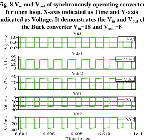
Output Voltage waveform for Boost Converter are shown in Figure 5. The Voltage of Power Semiconducting Switches for Boost Operation is shown in Figure 6. Input Current, Inductors Current and Capacitor Voltage for Boost converter are shown in figure 7. Input and Output Voltage waveform for Buck Converter is shown in figure 8. The voltage of power semiconducting switches for buck operation is shown in Figure 9. Input, Inductor current, and Vc for buck
[image:3.595.321.526.48.220.2]converter are shown in Figure 10.
Fig. 5 Vin and Vout of synchronously operating converter
for open loop. X-axis indicated as Time and Y-axis indicated as Voltage. It demonstrates the Vin and Vout of
the Boost converter Vin=18 and Vout =40
Fig. 6 Power Semiconducting Switches (sw1 and sw2) and
diodes (D1 and D2) Voltage of synchronously operating
[image:3.595.50.282.173.374.2]Buck-Boost Converter for open loop. It shows the Voltage during Boost operation
Fig. 7 Inductors and Capacitor Current and Voltage of synchronously operating Buck-Boost Converter for open loop. It shows the Current and Voltage during
[image:3.595.320.529.282.447.2]Boost operation
Fig. 8 Vin and Vout of synchronously operating converter
for open loop. X-axis indicated as Time and Y-axis indicated as Voltage. It demonstrates the Vin and Vout of
[image:3.595.49.281.438.653.2]the Buck converter Vin=18 and Vout =8
Fig. 9 Power Semiconducting Switches (sw1 and sw2) and
diodes (D1 and D2) Voltage of synchronously operating
[image:3.595.311.545.454.681.2]Fig. 10 Inductors and Capacitor Current and Voltage of synchronously operating Buck-Boost Converter for open loop. It shows the Current and Voltage during
Buck operation
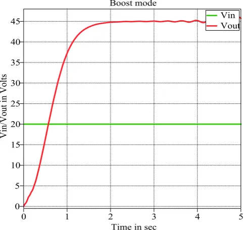
The closed-loop simulated waveform for Input and Output Voltage waveform for Boost Converter are shown in Figure11. The Voltage Power Semiconducting Switches are shown in Figure 12. Input Current and Capacitor Voltage are shown in Figure 13. Efficiency Comparisions among Existing and Proposed Method are shown in Figure 14.
Fig. 11 Vin and Vout of synchronously operating
Buck-Boost converter for closed loop. X-axis indicated as Time and Y-axis indicated as Voltage. It shows the Vin and Vout
of the Boost converter Vin=20 and Vout =45
Fig. 12 Power Semiconducting Switches (sw1 and sw2) and
diodes (D1 and D2) Voltage of synchronously operating
[image:4.595.310.547.54.266.2]Buck-Boost Converter for closed loop
Fig. 13 Inductors and Capacitor Current and Voltage of synchronously operating Buck-Boost Converter for
[image:4.595.309.544.309.508.2]closed loop
[image:4.595.51.293.455.683.2]International Journal of Innovative Technology and Exploring Engineering (IJITEE) ISSN: 2278-3075, Volume-8 Issue-5S March, 2019
IV. CONCLUSION
A modernized transformer less quadratic Buck-Boost Converter was suggested in this paper. Which enhance among the structure development and the Voltage increase to defeat the disadvantages of the conventional buck-boost converter. The working principles, steady-state investigations, little flag demonstrating and contrasted and distinctive converters. From the hypothetical examinations, the simulation and circuit demonstrated that the transformer-less buck-boost converter has the benefits of high advance-up/ venture down voltage increase, straightforward development, and basic control strategy. Thus, the developed buck-boost converter is appropriate for the Industrial usage requiring high advance-up/ venture down voltage increase. Truth is told a period time-continuous input current might be accomplished. This create the converter valuable for energy sources, for example, batteries and energy units, In addition two-arrange photovoltaic frameworks and in common to any power converter arrange requiring a time-continuous input current.
REFERENCES
1. D .Zhou, “Synthesis of PWM Dc-to-Dc Power Converters,” Ph.D. thesis, California Institute of Technology, October 1995.
2. P. Lee, Y. Lee, D. Cheng, and X. Liu,”Steady-State Analysis of an Interleaved Boost Converter with Coupled Inductors”, IEEE Trans. On Industrial Electronics, Vol. 47, No.4, August 2000, pp787-795. 3. B. Lin and H. Lu,”A Novel PWM Scheme for Single-Phase Three
Level Power-Factor-Correction Circuit”, IEEE Trans.On Industrial Electronics, Vol. 47, No. 2, April 2000
4. D. Maksimovic and R. Erickson,” Universal-Input, High-Power-Factor, Boost Doublers Rectifier”, Proc.IEEE APEC, 1995 Record, pp. 459-465.
5. D. Wolaver,”Fundamental Study of Dc to Dc Conversion System,”Ph.D. thesis, Massachusetts Institute of Technology, January 1969.
6. D. Maksimovic and S. Cuk,”General Properties and Synthesis of PWM Dc-to-Dc converters”, in IEEE Power Electronics Specialists Conference, pp.515-525, 1989.
7. D. Maksimovic and S. Cuk, “Switching Converters with wide Dc conversion range” ,IEEE Transaction on Power Electronics, Vol. 6, No. 1, pp.151-157, Jan.,1991
8. G. Moschopoulos, “Quadratic Power Conversion for industrial application”, APEC, pp. 1320-1327, 2010.
9. X. L. Wei, K. M. Tsang and W. L. Chan, “Non-linear PWM control of single-switch quadratic buck converters using internal model”, IET Power Electronics, Vol. 2, No. 5, pp.475-483, 2009.
![Fig. 3 Operational interval of Buck-Boost Converter Interval 1[NT<t< (N+D) T]](https://thumb-us.123doks.com/thumbv2/123dok_us/8215951.264202/2.595.56.272.226.339/fig-operational-interval-buck-boost-converter-interval-nt.webp)