Theses Thesis/Dissertation Collections
12-2014
Drowsy Cache Partitioning for Multithreaded
Systems and High Level Caches
Samantha Rose Kenyon
Follow this and additional works at:http://scholarworks.rit.edu/theses
This Thesis is brought to you for free and open access by the Thesis/Dissertation Collections at RIT Scholar Works. It has been accepted for inclusion in Theses by an authorized administrator of RIT Scholar Works. For more information, please [email protected].
Recommended Citation
by
Samantha Rose Kenyon
A Thesis Submitted in Partial Fulfillment of the Requirements for the Degree of Master of Science
in Computer Engineering
Supervised by
Assistant Professor Dr. Sonia Lopez Alarcon Department of Computer Engineering
Kate Gleason College of Engineering Rochester Institute of Technology
Rochester, New York December 2014
Approved by:
Dr. Sonia Lopez Alarcon, Assistant Professor
Thesis Advisor, Department of Computer Engineering
Dr. Amlan Ganguly, Assistant Professor
Committee Member, Department of Computer Engineering
Dr. Muhammed Shaaban, Associate Professor
Rochester Institute of Technology Kate Gleason College of Engineering
Title:
Drowsy Cache Partitioning for Multithreaded Systems and High Level Caches
I, Samantha Rose Kenyon, hereby grant permission to the Wallace Memorial Library to reproduce my thesis in whole or part.
Samantha Rose Kenyon
Dedication
Acknowledgments
I would like to thank my adviser, Dr. Sonia Lopez Alarcon. Without her guidance and support this work would not have been possible. I would also like to thank my committee members, Dr. Amlan Ganguly and Dr. Muhammed Shaaban. In addition, I would like like to thank my friends, Jason Lowden and Colin Donahue, for supporting me on this journey. They have always been there for me through many ups and downs and I would not have
made it this far without them. Finally, I would like to thank the Computer Engineering department. The department as a whole has provided me unending support and guidance
Abstract
Drowsy Cache Partitioning for Multithreaded Systems and High Level Caches
Samantha Rose Kenyon
Supervising Professor: Dr. Sonia Lopez Alarcon
Power consumption is becoming an increasingly important component of processor design. As technology shrinks both static and dynamic power become more relevant. This is par-ticularly important for the cache hierarchy. The cache portion of a microprocessor contains a large percentage of the total number of transistors in the microprocessor. Therefore the cache consumes a large percentage of both static and dynamic power. When improving power consumption in the past, there has always been a large trade-off between energy savings and performance.
Techniques that reduce power consumption typically have a negative impact on perfor-mance. Likewise, when performance is improved it is at the cost of higher energy con-sumption. Also many current implementations only reduce one kind of power in the cache, either static or dynamic. For a more robust approach that will remain relevant as technology continues to shrink, both aspects of power need to be addressed.
This thesis implements a phase adaptive cache that will reduce both static and dynamic power while having very little impact on the performance. This cache stores the most recently used blocks in one partition that is quick and easy to access. The second partition is placed in drowsy mode to reduce leakage power consumption. In this work, this approach is implemented for all three levels of cache in a multicore architecture. The design is also tested with multithreaded simulations. Brendan Fitzgeraldet al.used a similar approach in [10], however it was only for a second level cache for a single threaded application.
Contents
Dedication. . . iii
Acknowledgments . . . iv
Abstract . . . v
1 Introduction. . . 1
2 Supporting Work . . . 4
2.1 Previous Work . . . 4
2.1.1 Selective Cache Ways . . . 4
2.1.2 Cache Hierarchy Reconfiguration . . . 6
2.1.3 Accounting Cache . . . 9
2.1.4 Phase Adaptive Cache . . . 10
2.1.5 Drowsy Cache . . . 12
2.1.6 Temporal Locality for Drowsy Caches . . . 13
2.2 Related Work . . . 14
2.2.1 MorphCache . . . 15
2.2.2 Efficient Cache Resizing . . . 16
2.2.3 DRG-Cache . . . 17
2.2.4 Location Cache . . . 18
2.2.5 Application Specific Low Leakage Cache . . . 20
2.2.6 Multi-Core Analysis . . . 21
2.3 Summary . . . 21
3 Drowsy Phase Adaptive Cache for L1, L2, and L3 On-Chip Cache . . . 22
3.1 Drowsy Phase Adaptive Cache . . . 22
3.1.1 Cost Functions . . . 26
4 Methodology . . . 28
4.1 SPICE . . . 28
4.2 CACTI . . . 29
4.2.1 Latency . . . 30
4.2.2 Energy and Power . . . 35
4.3 Multi2sim . . . 40
4.3.1 Simulation Configurations . . . 42
4.3.2 Benchmarks . . . 42
4.4 Summary . . . 43
5 Results. . . 45
5.1 Experiments . . . 45
5.2 Single Threaded Results . . . 46
5.2.1 L1 Results . . . 46
5.2.1.1 Performance . . . 46
5.2.1.2 Energy and Power . . . 49
5.2.2 L2 Results . . . 52
5.2.2.1 Performance . . . 52
5.2.2.2 Energy and Power . . . 55
5.2.3 L3 Results . . . 58
5.2.3.1 Performance . . . 58
5.2.3.2 Energy and Power . . . 60
5.2.4 L1, L2, L3 Single Threaded . . . 63
5.2.4.1 Performance . . . 63
5.2.4.2 Energy and Power . . . 66
5.3 Multithreaded Results . . . 73
5.3.1 L1 and L2 Multithreaded Results . . . 73
5.3.1.1 Performance . . . 73
5.3.1.2 Energy and Power . . . 76
5.3.2 L1 and L3 Multithreaded Results . . . 79
5.3.2.1 Performance . . . 80
5.3.2.2 Energy and Power . . . 82
5.3.3 L2 and L3 Multithreaded Results . . . 85
5.3.3.1 Performance . . . 86
5.3.3.2 Energy and Power . . . 88
5.3.4 L1, L2, L3 Multithreaded Results . . . 92
5.3.4.2 Energy and Power . . . 96
5.4 Multicore Results . . . 101
5.4.0.3 Performance . . . 101
5.4.0.4 Energy and Power . . . 107
5.5 Summary . . . 115
6 Conclusions . . . 116
Bibliography . . . 117
A Multithreaded Results . . . 120
A.1 L1 Multithreaded Results . . . 120
A.1.1 Performance . . . 120
A.1.1.1 Configuration Time . . . 120
A.1.1.2 Speedup and IPC . . . 121
A.1.2 Energy and Power . . . 123
A.1.2.1 Dynamic Energy . . . 123
A.1.2.2 Leakage Energy . . . 123
A.1.2.3 Total Energy . . . 124
A.2 L2 Multithreaded Results . . . 125
A.2.1 Performance . . . 125
A.2.1.1 Configuration Time . . . 125
A.2.1.2 Speedup and IPC . . . 126
A.2.2 Energy and Power . . . 128
A.2.2.1 Dynamic Energy . . . 128
A.2.2.2 Leakage Energy . . . 128
A.2.2.3 Total Energy . . . 129
A.3 L3 Multithreaded Results . . . 130
A.3.1 Performance . . . 130
A.3.1.1 Configuration Time . . . 130
A.3.1.2 Speedup and IPC . . . 131
A.3.2 Energy and Power . . . 132
A.3.2.1 Dynamic Energy . . . 132
A.3.2.2 Leakage Energy . . . 133
List of Tables
3.1 Possible configurations of 4 way cache hierarchy . . . 23
3.2 Possible configurations of 8 way cache hierarchy . . . 23
3.3 Possible configurations of 16 way cache hierarchy . . . 23
4.1 CACTI latency results for L1 . . . 31
4.2 Possible configurations and latency of L1 . . . 32
4.3 CACTI latency results for L2 . . . 32
4.4 Possible configurations and Latency for L2 . . . 32
4.5 CACTI latency results for L3 . . . 33
4.6 Possible configurations and Latency for L3 . . . 34
4.7 CACTI L1 Energy Results . . . 35
4.8 CACTI L1 Final Energy Results . . . 37
4.9 CACTI L2 Energy Results . . . 38
4.10 CACTI L3 Energy Results . . . 38
4.11 CACTI L3 Final Energy Results . . . 40
4.12 Memory Configurations for All Simulations . . . 42
4.13 Processor Configuration . . . 42
4.14 Spec2006 Benchmarks Used [6] . . . 44
4.15 Spec2006 Benchmark Performance Numbers . . . 44
5.1 Simulation Configurations and Descriptions . . . 45
5.2 Access Costs for L3 Configurations . . . 68
5.3 Experiments with Four Threads . . . 92
List of Figures
2.1 Hardware Design for a Single Way in a Selective Way Cache [3] . . . 5
2.2 Example Partitioning for 256KB Banks [5] . . . 7
2.3 Possible Cache Configurations for a single 256KB structure [5] . . . 8
2.4 Possible configurations of a 4-way cache and swapping blocks [7] . . . 9
2.5 Different Clock Domains within Phase Adaptive Cache Design [8] . . . 11
2.6 Drowsy memory circuit diagram [11] . . . 12
2.7 Drowsy Cache Line Implementation Logic [11] . . . 14
2.8 MorphCache Example Four Core Topology [18] . . . 15
2.9 Resizable Cache Architecture [13] . . . 16
2.10 DRG-Cache Gated-Ground Transistor [1] . . . 18
2.11 Location Cache Example Hierarchy [15] . . . 19
3.1 Example of cache partitioning [10] . . . 24
3.2 Example access pattern with MRU counters and states [10] . . . 25
4.1 SRAM Cell used for SPICE simulations [10] . . . 29
4.2 SPICE Simulation Results . . . 29
4.3 Plot and equation for L1 Latency . . . 31
4.4 Plot and equation for L2 Latency . . . 33
4.5 Plot and equation for L3 Latency . . . 34
4.6 L1 Energy Plot and Equations . . . 36
4.7 L2 Energy Plot and Equations . . . 37
4.8 L3 Energy Plot and Equations . . . 39
4.9 Multiple Core Configuration [2] . . . 43
5.1 L1 Config Distributions . . . 47
5.2 Speedup of L1 Simulations . . . 48
5.3 L1 MRU Distributions . . . 49
5.4 Total Dynamic Energy Savings of L1 Simulations . . . 50
5.5 Total Leakage Energy of L1 Simulations . . . 51
5.6 Total Energy Savings of L1 Simulations . . . 52
5.8 Speedup of L2 Simulations . . . 54
5.9 L2 MRU Distributions . . . 55
5.10 Total Dynamic Energy Savings of L2 Simulations . . . 56
5.11 Total Leakage Energy of L2 Simulations . . . 57
5.12 Total Energy Savings of L2 Simulations . . . 57
5.13 L3 Config Distributions . . . 58
5.14 Speedup of L3 Simulations . . . 59
5.15 L3 MRU Distributions . . . 60
5.16 Total Dynamic Energy Savings of L3 Simulations . . . 61
5.17 Total Leakage Energy of L3 Simulations . . . 62
5.18 Total Energy Savings of L3 Simulations . . . 62
5.19 L1 Config Distributions . . . 63
5.20 L2 Config Distributions . . . 64
5.21 L3 Config Distributions . . . 65
5.22 Speedup . . . 66
5.23 Total Dynamic Energy Savings of L1 Cache . . . 67
5.24 Total Dynamic Energy Savings of L2 Cache . . . 67
5.25 Total Dynamic Energy Savings of L3 Cache . . . 69
5.26 Total Leakage Energy of L1 Cache . . . 69
5.27 Total Leakage Energy of L2 Cache . . . 70
5.28 Total Leakage Energy of L3 Cache . . . 70
5.29 Total Energy Savings of L1 Cache . . . 71
5.30 Total Energy Savings of L2 Cache . . . 72
5.31 Total Energy Savings of L3 Cache . . . 72
5.32 L1 Config Distributions . . . 74
5.33 L2 Config Distributions . . . 75
5.34 Speedup . . . 76
5.35 Total Dynamic Energy Savings of L1 Cache . . . 76
5.36 Total Dynamic Energy Savings of L2 Cache . . . 77
5.37 Total Leakage Energy of L1 Cache . . . 78
5.38 Total Leakage Energy of L2 Cache . . . 78
5.39 Total Energy Savings of L1 Cache . . . 79
5.40 Total Energy Savings of L2 Cache . . . 79
5.41 L1 Config Distributions . . . 80
5.42 L3 Config Distributions . . . 81
5.44 Total Dynamic Energy Savings of L1 Cache . . . 82
5.45 Total Dynamic Energy Savings of L3 Cache . . . 83
5.46 Total Leakage Energy of L1 Cache . . . 84
5.47 Total Leakage Energy of L3 Cache . . . 84
5.48 Total Energy Savings of L1 Cache . . . 85
5.49 Total Energy Savings of L3 Cache . . . 85
5.50 L2 Config Distributions . . . 86
5.51 L3 Config Distributions . . . 87
5.52 Speedup . . . 88
5.53 Total Dynamic Energy Savings of L2 Cache . . . 89
5.54 Total Dynamic Energy Savings of L3 Cache . . . 89
5.55 Total Leakage Energy of L2 Cache . . . 90
5.56 Total Leakage Energy of L3 Cache . . . 90
5.57 Total Energy Savings of L2 Cache . . . 91
5.58 Total Energy Savings of L3 Cache . . . 91
5.59 L1 Config Distributions . . . 93
5.60 L2 Config Distributions . . . 94
5.61 L3 Config Distributions . . . 95
5.62 Speedup . . . 96
5.63 Total Dynamic Energy Savings of L1 Cache . . . 97
5.64 Total Dynamic Energy Savings of L2 Cache . . . 97
5.65 Total Dynamic Energy Savings of L3 Cache . . . 98
5.66 Total Leakage Energy of L1 Cache . . . 98
5.67 Total Leakage Energy of L2 Cache . . . 99
5.68 Total Leakage Energy of L3 Cache . . . 99
5.69 Total Energy Savings of L1 Cache . . . 100
5.70 Total Energy Savings of L2 Cache . . . 100
5.71 Total Energy Savings of L3 Cache . . . 101
5.72 L1-1 Config Distributions . . . 102
5.73 L1-2 Config Distributions . . . 103
5.74 L2-1 Config Distributions . . . 104
5.75 L2-2 Config Distributions . . . 105
5.76 L3 Config Distributions . . . 106
5.77 Speedup . . . 107
5.78 Total Dynamic Energy Savings of L1-1 Cache . . . 107
5.80 Total Dynamic Energy Savings of L2-1 Cache . . . 108
5.81 Total Dynamic Energy Savings of L2-2 Cache . . . 109
5.82 Total Dynamic Energy Savings of L3 Cache . . . 109
5.83 Total Leakage Energy of L1-1 Cache . . . 110
5.84 Total Leakage Energy of L1-2 Cache . . . 110
5.85 Total Leakage Energy of L2-1 Cache . . . 111
5.86 Total Leakage Energy of L2-2 Cache . . . 111
5.87 Total Leakage Energy of L3 Cache . . . 112
5.88 Total Energy Savings of L1-1 Cache . . . 112
5.89 Total Energy Savings of L1-2 Cache . . . 113
5.90 Total Energy Savings of L2-1 Cache . . . 113
5.91 Total Energy Savings of L2-2 Cache . . . 114
5.92 Total Energy Savings of L3 Cache . . . 114
A.1 L1 Config Distributions . . . 121
A.2 Speedup for L1 Simulations . . . 122
A.3 L1 MRU Distributions . . . 122
A.4 Total Dynamic Energy Savings of L1 Simulations . . . 123
A.5 Total Leakage Energy of L1 Simulations . . . 124
A.6 Total Energy Savings of L1 Simulations . . . 124
A.7 L2 Config Distributions . . . 126
A.8 Speedup of L2 Simulations . . . 127
A.9 L2 MRU Distributions . . . 127
A.10 Total Dynamic Energy Savings of L2 Simulations . . . 128
A.11 Total Leakage Energy of L2 Simulations . . . 129
A.12 Total Energy Savings of L2 Simulations . . . 129
A.13 L3 Config Distributions . . . 130
A.14 Speedup of L3 Simulations . . . 131
A.15 L3 MRU Distributions . . . 132
A.16 Total Dynamic Energy Savings of L3 Simulations . . . 133
A.17 Total Leakage Energy of L3 Simulations . . . 133
Chapter 1
Introduction
As manufacturing technology is improved and transistors shrink, the number of transistors
on a chip has increased exponentially. Power consumption has now become a major factor
in microprocessor design. Performance improvements in current designs are limited by
their power consumption and therefore improvements in speed have diminished over the
years.
Memory elements in a microprocessor do not improve as fast as processors. Due to this
bottleneck, a large percentage of transistors are used to increase the size of local storage,
the cache hierarchy. This directly results in the cache consuming a large percentage of
overall power in the microprocessor. The cache hierarchy contains up to 35% of the total
number of transistors on a processor [10], making power consumption within the cache
critical.
Previous efforts have focused on either static power or dynamic power consumption,
ap-plying techniques that modify the architecture, the circuit design, or the actual transistor
manufacturing. Also previous efforts have either focused on increasing performance or
reducing energy due to the inherent trade-offs between the two. An increase in
consumption will correlate to a decrease in performance. This work looks to use a
combi-nation of techniques to reduce both static and dynamic power while only slightly reducing
the performance. By combining transistor level circuit analysis and cache architecture,
both static and dynamic power can be saved with an acceptable performance hit.
This is done using the drowsy cache partitioning scheme proposed previously and
imple-mented in the second level cache [10]. This work exploits the temporal locality of cache
memory in which 92% of all cache accesses are made to the most recently used (MRU)
cache line. Extending that idea shows that 98% of accesses are made to the two most
re-cently used cache lines [16]. This information can then be used to design a cache hierarchy
with two partitions. One partition, the A partition, remains in an active state, while the
other partition, the B partition, is in a drowsy state. The partitions are also phase adaptive
and can therefore determine the ideal cache partitions using cost functions. There are
mul-tiple cost functions based on either the energy consumption or the energy-delay product.
Although each partition can dynamically alter its associativity the total set associativity of
the cache remains unchanged.
This cache design saves dynamic power by accessing the A partition first, which is only
a portion of the total cache, and then accessing the B partition only when the data needed
is not found in the A partition. The most recently used blocks are kept in A by swapping
data between partitions. When the data is not found in A but is found in B, that data is then
placed in the A partition and swapped with the least recently used block found in A. The
same is done for data found in other levels of cache.
This design also saves static power because the B partition is placed in a drowsy state. This
means that the B partition is kept at a lower voltage. This lower voltage is low enough
allows for a modest decrease in the overall performance and reduces the overall static power
consumption of the cache hierarchy.
In this work, this cache design is applied to all three levels of the cache in both
multi-threaded and multicore architectures. Due to the differences in accesses, size, and behavior
it is useful to look at the affect this design will have on both energy and performance for
all three levels.
The rest of this thesis is organized as follows: Chapter 2 discusses supporting work as well
as previous designs that have been proposed. Chapter 3 outlines the proposed design for
the drowsy phase adaptive cache. Chapter 4 explains the implementation of this design as
well as the testing and simulation environment. Chapter 5 shows results for single threaded,
multithreaded, and multicore simulations. Finally, Chapter 6 provides conclusions that can
Chapter 2
Supporting Work
There have been many advancements in cache architecture design through the years.
The-ses advancements have allowed for new cache designs and implementations, including what
is proposed here. Many of these works laid the foundation for low-power cache design,
while others focus on high-performance design. The ideas presented here are extended and
applied in ways similar to the work presented in this thesis and have been instrumental in
this cache design.
2.1
Previous Work
2.1.1 Selective Cache Ways
The idea of selective cache ways[3], first presented by Albonesi, was the first step in the development of phase adaptive cache hierarchies. In this hierarchy, a controller is used to
turn on and off certain cache ways. The number of ways being used at any given time is
dependent upon the number of instructions per cycle (IPC). As the IPC decreases, the
num-ber of ways being used increases to improve the performance. This is implemented with
hardware and software modifications. Figure 2.1 shows the hardware modifications that
need to be made to a basic cache. There are no modifications made to the tag portion of the
hardware. The data portion represents roughly 90% of the entire cache power dissipation,
It can be seen in Figure 2.1 that the data is divided into four separate way elements. A
Cache Way Select Register (CWSR) contains one bit for each of those ways to indicate
which ways to enable. This information is then sent to the cache controller which enables
or disables the appropriate ways. When a way is disabled no data is selected from that way
[image:19.612.112.510.224.576.2]and therefore that way essentially dissipates no dynamic power.
Figure 2.1: Hardware Design for a Single Way in a Selective Way Cache [3]
A Performance Degradation Threshold (PDT) is used here to determine when to enable and
disable certain ways. This is set to either 2%, 4%, or 6%. When the IPC is projected to
fall below this threshold with the current system, an additional way is then enabled. This
to obtain a desired performance.
This implementation was very successful and reduced dynamic cache energy dissipation
by 40% while only incurring a 2% performance hit. It is only reducing dynamic power
however, and is not sufficient as static power becomes more important.
2.1.2 Cache Hierarchy Reconfiguration
The implementation in [3] is inherently limiting because it only allows for enabling or
disabling a single way as the IPC changes. This does not take into account situations in
which an application would transition from very low cache activity to very high cache
activity [5]. This can occur often within a given application, especially when thrashing
occurs. Balasubramonian et al. in [5], attempts to enhance Albonesi’s design in [3], by removing this limitation.
In [5] Balasubramonianet al. implement a cache that can be dynamically reconfigured by implementing a one level cache at the physical layer and a two level virtual cache structure.
This is done by taking a 2MB cache and splitting it into two 1MB banks. These banks
are then broken down even farther into 256KB banks. This design for the 256KB banks is
shown in Figure 2.2.
The figure in Figure 2.3 shows the possible ways to partition a cache structure with one
physical level and two virtual levels for a single 256KB structure. Each block in Figure 2.3
represents a 128KB cache bank. Each of these banks has a top line that behaves like a direct
mapped level 1 cache. The bottom line then behaves like a two-way set associative level 1
cache. This structure replaces the traditional cache structure. It also allows for reduction
in energy dissipation while maintaining the same overall cache size with just a reduction in
Figure 2.2: Example Partitioning for 256KB Banks [5]
The access protocol for this cache set up varies from [3]. When there is a hit in L1 a single
way is being accessed and the data is returned. When there is a miss in L1 all of the tag
arrays of L2 are now read in parallel to increase performance. If the data is found in L2
then the block is swapped with the block in the specific way of L1 and the location where
the data was found in L2. If the data is not found in L2 the data currently in the specified
way of L1 is moved to L2 and new data is moved into L1. This guarantees that the cache is
non-inclusive.
The cache is first initialized to the smallest possible size which is a direct mapped 256KB
Figure 2.3: Possible Cache Configurations for a single 256KB structure [5]
to the accepted tolerance levels. The tolerance rates of this designed are based on the
IPC as well as the miss rate and the branch frequency. When the cache does not reach
the accepted tolerance rates the cache size is increased to the next largest size. This will
continue until the cache reaches the maximum size or all of the current working sets fit
within the configuration. The configuration is then set to stable after the number of misses
and branches remains stable. If the configuration then changes out of the stable state and is
set to be unstable then the cache is again set to the smallest configuration. Figure 2.3 shows
a detailed view of this process for a L1/L2 setup.
This implementation reduced the Cycles Per Instruction (CPI) by 15% when setup for
L1/L2 design. It also was able to reduce energy dissipation by 43% when setup for L2/L3
2.1.3 Accounting Cache
The accounting cache [7] represents another contribution to low power cache design. This
design is intended to leverage locality and LRU data rather than IPC to dynamically change
the cache structure, reducing dynamic power. This implementation requires MRU counters
for each of the number of ways in the cache. These counters keep track of the number of
hits at each of these ways. This implementation keeps track of the energy and performance
cost of the cache based on the current configuration. Performance Degradation Threshold
(PDT) is also used here to determine when to change cache configurations. They values
used for this system are 1.5%, 6.2%, and 25%.
The overall system is divided into two partitions; the A partition and the B partition. The
number of ways in each partition determines the current configuration. Figure 2.4 shows
the possible configurations for a 4-way cache of this type and also swapping of the cache
blocks.
Figure 2.4: Possible configurations of a 4-way cache and swapping blocks [7]
The access protocol is modified here to account for accessing both partitions. First the
A partition is accessed. If the block is found in A, the corresponding MRU counter is
partition is then searched along with the next level in the cache hierarchy. If the data
is found in the B partition, the corresponding MRU counter is updated and the block is
returned. The block is also swapped into the A partition at this time, with the LRU block
in the A partition. If the data is not found in B, but is found in the next level of the cache
hierarchy, then this block displaces the LRU block of the A partition. This displaced block
then replaces the LRU block of the B partition. The displaced block from the B partition is
then written to the next level. This design ensures that the A partition always contains the
most recently used blocks.
This LRU based design provides additional information if the data is expressed using its
dual, the most recently used (MRU) ordering. The most recently used way is referred to
as MRU 0 and then next most recently used way is referred to as MRU 1 and so on. This
means that hits to either MRU 0 or MRU 1 would represent a hit in a 2-way set associative
cache. This idea can then be extended to determine the hit ratio for any partitioning of the
cache system. The hits that occur in each MRU state provide the hit information for each
partition and can therefore be used to determine the next optimal configuration.
This design is successful, resulting in about a 30% energy savings in L1 and a 60% energy
savings in L2. This implementation, however does not reduce static power.
2.1.4 Phase Adaptive Cache
The accounting cache was then refined into a Phase-Adaptive Cache [8]. This cache
dy-namically adjusts its size and speed based on previous use, to increase performance. This
design is asynchronous while allowing for different operating frequencies within domains
within a processor resulting in a locally synchronous (GALS) design. Figure 2.5 shows the
Figure 2.5: Different Clock Domains within Phase Adaptive Cache Design [8]
Each section of Figure 2.5 is operating with a different clock period. This allows each of
these pieces to run at a different operating frequency. The latency for the A partition can
therefore remain the same while the frequency is modified. This means that when the A
partition is at its smallest the frequency of the system is at its greatest, which results in a
large variation in the latency to access the B partition. When the size of the A partition is
small, the latency to B can be three or more times as high.
The phase-adaptive cache is compared against a program-adaptive cache as well as a static
cache design. The program-adaptive cache changes from benchmark to benchmark but
does not dynamically change during benchmark execution. Of the three designs, the static
cache design performs the worst. The phase-adaptive cache outperforms the
program-adaptive cache, in most cases. The program-program-adaptive cache does perform better than the
and the higher branch prediction accuracy present in the program-adaptive implementation.
2.1.5 Drowsy Cache
There is one method that has been explored for reducing static power. All of the previous
works explored focus on reducing dynamic power, however, as technology sizes shrink
below 0.1 µm static power will begin to dominate the total power dissipation [14]. The
Drowsy Cache design [11] is able to significantly reduce leakage power, with a minimal
performance penalty. This involves putting a SRAM cell in a drowsy state to try and reduce
subthreshold leakage. The drowsy memory circuit is shown in Figure 2.6.
Figure 2.6: Drowsy memory circuit diagram [11]
The drowsy circuit shows an SRAM cell that either receives the normal power supply
voltage or it receives a lower voltage. Dynamic voltage scaling (DVS) can be used to
lower the supplied voltage to the SRAM cell while preserving its state as shown in [14].
This is very important because preserving the state allows for less of a penalty and less of
There are two cross-coupled inverters in the SRAM cell as shown in Figure 2.6. This
results in two different leakage current paths. The dominate current can be modeled as
shown below:
ID =Ise
VGS−VT
nkT /q (1−e− VDS
kT /q)(1 +λV
DS) (2.1)
where λ is the channel-length modulation parameter. The overall leakage current is then
derived from Equation 2.1 and is shown below:
IL= ((ISN +ISP) + (ISNλN +ISPλP)VDD)×(1−e −nkT /qVDD
) (2.2)
whereISN andISP represent the nMOS and pMOS off-transitor current factors independent
from Equation 2.1. From Equation 2.2 it can be seen that IL depends largely on VDD.
Therefore a slight reduction inVDD will have a large impact on the leakage current within
the SRAM cell. From there Kim et al. choose a voltage that is 50% higher than their
threshold voltage. This is to guarantee that the state of the data is preserved and is a
conservative approximation. With this, drowsy voltage leakage is reduced by about 80%.
To implement this drowsy cache design additional logic is needed around the SRAM cell.
Figure 2.7 shows the logic required for a single drowsy cache line.
The Drowsy state allows for a lower performance penalty than if the design had a gated
VDD. If the tag array design is normal then there is just a 1 cycle penalty to raise the voltage
on the cache line to read the data. If the tag array also uses drowsy SRAM cells then there
is a 3 cycle penalty to raise the voltage in the line. This cache design allows for a 50%
reduction in energy used by the cache design with a very small decrease in performance.
2.1.6 Temporal Locality for Drowsy Caches
There has also been important research done about temporal locality in caches specifically
Figure 2.7: Drowsy Cache Line Implementation Logic [11]
determine how to best use a drowsy cache design. They found that the majority of the
accesses to the cache occur to the blocks that are most recently used, specifically the most
recently used states 0 and 1. When looking at the first MRU line they found 92% of the
total hits occurred there. When extending this to the second MRU line they found 98%
of the total hits occurred there. This information can therefore be used to safely determine
which areas of the cache to put into a drowsy state to incur the smallest performance penalty
possible.
2.2
Related Work
There are others who have tried to do similar work using these existing results. Most of
the existing implementations are designed to either save static or dynamic power. The
implementation proposed here strives to save both dynamic and leakage power. Previous
incur a much higher performance hit than the design presented here.
2.2.1 MorphCache
Srikantaiah et al. propose a reconfigurable adaptive multi-level cache design called a
MorphCache [18]. This cache dynamically changes the cache hierarchy to improve per-formance. The initial configuration is per-core L2 and L3 cache slices. From there the
MorphCache either merges slices or splits them, dynamically, to change the slices and
configurations available to each core.
Figure 2.8: MorphCache Example Four Core Topology [18]
Figure 2.8 shows a MorphCache for a system with four cores where each core has a private
L1 and close access to L2 and L3 slices. Figure 2.8 also shows that the MorphCache is
capable of adapting into both a symmetric and asymmetric topology.
The MorphCache will merge slices when either one slice is highly-utilized while the other
is under-utilized, or both are highly-utilized and shared by threads sharing the same address
space. Merging must be done carefully though, because merging two L2 slices when L3
slices are split, could result in the L2 capacity being larger than L3. To avoid this the
splitting slices it is necessary to ensure that splitting L3 does not results in a smaller L3
than L2 similar to the merging requirements. Therefore, the MorphCache only splits L3 if
the corresponding merged L2 slices can be split as well.
This implementation is focused on improving performance. The work proposed here differs
from this because it is focused on saving power with a small performance hit. Also the
MorphCache requires modifications to the interconnection network where as the proposed
design does not.
2.2.2 Efficient Cache Resizing
Keramindas et al. proposes a new framework for efficient cache resizing in terms of both power and performance [13]. The cache proposed here dynamically reconfigures memory
based on the behavior of the running application. Figure 2.9 shows the overall architecture
for this cache design.
The two mask registers, set-mask and way-mask, control both the horizontal and vertical
resizing. Each bit in the way-mask register controls enabling and disabling that
corre-sponding cache way. For horizontal resizing additional cache access logic is needed. The
number of sets, in a conventional cache, defines both the tag bits and index used to look up
and place a cache block. The set-mask registersis used to ensure that the correct number of index bits is being used for a particular cache size. When downsizing, the number of index
bits decreases and vice versa. The number of tag bits increases as cache size decreases,
therefore there must be as many tag bits as needed for the smallest cache size possible for
this design.
In a typical resizing cache, when the cache size is decreased the discarded part of the
cache is immediately deactivated. Instead, here the discarded part is kept active and they
gradually deactivate. When all of these parts are deactivated, the transition has officially
completed. This protects against miss rate hiccups that generally occur immediately after
resizing. This can severely hurt performance. Overall this method results in cache size
reduction of anywhere from 13% to 30% with a very low performance impact of 4% to
10%.
This work focuses on reducing the area of a cache in a way that is efficient in terms of both
energy and performance. The implementation proposed here differs from this because it
focuses saving leakage and dynamic energy, by modifying the cache configuration, while
keeping the cache area the same.
2.2.3 DRG-Cache
Agrwal et al. proposes a Data Retention Gated-Ground Cache, or a DRG-Cache. This
cache uses gated-ground techniques to reduce leakage power consumption in cache
the ground line and the SRAM cell. This allows for the supply voltage to be effectively
off, substantially reducing leakage energy dissipation. In the DRG-Cache this transistor is
connected to the row decoder which then signals which cells are in standby mode, where
the supply is effectively off, and which are in active mode. This design is shown in Figure
2.10.
Figure 2.10: DRG-Cache Gated-Ground Transistor [1]
This technique allows for a large reduction in leakage energy, however it increases dynamic
energy for read and write operations. Also, turning off the supply voltage results in the
pos-sibility of destroying data stored in the SRAM cell. Another component to this technique
is determining the optimal size of this Gated-Ground transistor. Increasing the size of this
transistor improves performance as well as data retention but lowers the overall power
sav-ings. Since data retention is very important in this application the total energy savings is
limited because the size of the transistor will remain large to retain data. The work
pro-posed here differs from this because it is state-preserving. Also the propro-posed work aims to
save both dynamic and leakage power whereas this work only saves leakage power while
increasing dynamic energy.
2.2.4 Location Cache
Jason Nemeth et al. proposes a location cache that has a low power second level cache, using gated-ground techniques [15]. Combining these two ideas, the goal is to save on
both static and dynamic power. This second level is using the gated-ground techniques
low power structure with a location cache. This location cache is a direct-mapped cache
that provides the second level cache with accurate access way location information. The
additional cache runs in parallel with the L1 cache. This reduces L2 power consumption
more than the typical set-associative cache. This memory hierarchy is shown in Figure
2.11.
Figure 2.11: Location Cache Example Hierarchy [15]
The access pattern for this cache first determines if there is a hit in L1. If there is, the result
obtained from the location cache, running in parallel, is discarded. If there is a miss in
L1 and a hit in the location cache, L2 is accessed as a direct-mapped cache, reducing the
access power. If there is a miss in both L1 and the location cache, then L2 is accessed as
a conventional set-associative cache. In this case the data in the location cache is updated.
This idea is further extended to work with multicore architectures. There are two ways to
all cores share only one location cache. This implementation is shown to save between 2%
and 43% of total power, however it has the same limitations as the DRG-Cache [1] because
it uses the same gated-ground technique.
2.2.5 Application Specific Low Leakage Cache
Farahaniet al.proposes a modification to the general drowsy cache configuration [9]. This work proposes two different methods for saving leakage in a cache. In the first design,
cache words are placed in a drowsy mode at the end of a period of time called an update
window (UW). When a word is needed, only that word is brought back up to an active
voltage level and the rest of the cache line remains in a drowsy state. In this design, they
are able to save on the penalty of activating the entire line while still saving energy by
keeping the other words in the line in a drowsy state. This could, however, perform worse
than the standard drowsy cache if more than one word in the cache line is needed. In this
case, the penalty will be higher for waking up more than one word, than if the entire cache
line had been activated.
The second approach identifies active words and does not place them into the drowsy mode
at the end of a UW. This allows for a performance savings as well as leakage savings, with
the words that are placed in the drowsy state. A single status-bit is used here to record
whether or not a word is active. This bit is set high when a word is read and at the end of
a UW all words with a status-bit of zero are placed in the drowsy state. At the end of the
next UW the status-bit is set to zero.
The first implementation reduces leakage power by an average of 88% with an average
performance loss of just 0.7%. The second implementation reduces leakage power by an
average of 89% with an average performance loss of 0.5%. Although this implementation
dynamic power at all.
2.2.6 Multi-Core Analysis
Jorge Albericio [2] has recently purposed a reuse cache. This cache uses locality to only
store data that is prone to being reused. Jorge Albericio’s work focuses on multicore
archi-tectures in which the last level of cache is shared among multiple cores. He proposes using
reuse locality, rather than temporal locality, along with modified least recently used (LRU)
and not recently used (NRU) replacement policies. These modified replacement policies,
least recently reused (LRR) and not recently reused (NRR), perform better than their
coun-terparts (LRU and NRU) in a multicore system with a high workload. This work explores
locality in a shared cache multicore environment, however it does not propose an energy
savings. The architecture used here will be used to also test the drowsy phase adaptive
cache in a multicore environment.
2.3
Summary
This chapter discussed supporting work that is related to the work presented here. It also
presented previous work that has attempted to achieve similar goals. These previous works
aim to save power in the memory hierarchy while incurring a small performance penalty.
The next chapter provides an in depth explanation of the design proposed in this work. It
Chapter 3
Drowsy Phase Adaptive Cache for L1, L2, and
L3 On-Chip Cache
The drowsy phase adaptive cache presented in this thesis is a combination of the phase
adaptive cache and the drowsy cache. The phase adaptive cache attempts to save dynamic
power while incurring a modest performance penalty. The drowsy cache attempts to save
leakage energy while again incurring a small performance hit. The drowsy phase adaptive
cache combines these designs to save both dynamic power and leakage power in the cache
while incurring a small performance penalty. This work extends upon the drowsy phase
adaptive cache proposed in [10] to multithreaded and multicore applications as well as all
levels of cache.
3.1
Drowsy Phase Adaptive Cache
The accounting cache proposed in [7] is reduced for this work limiting the possible
config-urations to powers of two. The number of possible configconfig-urations will vary based on the
associativity of each cache level. For a four way set-associative cache, the configurations
are 1/3, 2/2, and 4/0, where each number represents A/B partitions as shown in Table 3.1.
These configurations will be referenced as C0, C1, and C2.
Name A partition B partition
C0 1-way 3-way
C1 2-way 2-way
C2 4-way 0-way
Table 3.1: Possible configurations of 4 way cache hierarchy
referenced as C0, C1, C2, and C3 as shown in Table 3.2.
Name A partition B partition
C0 1-way 7-way
C1 2-way 6-way
C2 4-way 4-way
C3 8-way 0-way
Table 3.2: Possible configurations of 8 way cache hierarchy
Finally, for a 16 way set-associate cache the configurations are 1/15, 2/14, 4/12, 8/8, 16/0
which will be referenced as C0, C1, C2, C3, C4 as shown in Table 3.3.
Name A partition B partition
C0 1-way 15-way
C1 2-way 14-way
C2 4-way 12-way
C3 8-way 8-way
C4 16-way 0-way
Table 3.3: Possible configurations of 16 way cache hierarchy
This allows for different possible configurations that resize the A partition to powers of
two. These three associativities will be the total associativity of the different cache levels.
Cache level 1 will be a 4 way set-associative cache, while level 2 will be an 8 way-set
associative cache, while level 3 will have 16 ways. The total number of ways in the cache
never changes, however, the different configurations allow for each partition to have a
varying number of ways. Figure 3.1 shows an example for the different number of ways
each partition can have. This example is for the second cache level. In this figure the yellow
area represents partition A and the green area represents partition B. Notice that in the C0
however partition B is fully phase adaptive with a total of 7 ways.
Figure 3.1: Example of cache partitioning [10]
The access protocol for this cache design takes advantage of the dual partition structure.
The cache first looks for the necessary data in the A partition. MRU counters are used to
control when the cache changes between different configurations. If the data is found in
the A partition, a corresponding MRU counter is updated and the data is returned. If the
data is not found in A, the B partition is searched. If it is found in the B partition, the MRU
counter is updated and this block is then swapped into the A partition. If the data is not
found in the B partition and is found in the next level, then the block is brought up to the A
partition and a block from the A partition is evicted into the B partition. A block from the
B partition is then also evicted into the next level. After this the MRU states are updated to
reflect the changing states. Figure 3.2 shows an example access pattern with updates to the
MRU counters and states for a 4-way set-associate cache.
The blocks of color show the current MRU state. MRU state 3 is equivalent to the least
recently used state (LRU). First, block B is accessed and its MRU counter is increased.
Since this data is located in the A partition, the green area, this is all that is necessary.
From there, block C is accessed and the MRU state counter is incremented. In this case,
that is the counter for MRU state 2 represented by the purple block. However block C is in
the B partition, therefore C needs to be swapped into A. From there C is accessed again and
Figure 3.2: Example access pattern with MRU counters and states [10]
represented by the yellow block, because it was swapped with A. C was swapped because
it was the most recently used block, which always needs to be kept in the A partition. A
was chosen because A was the least recently used block in the A partition. Finally D is
accessed and the counter for MRU state 3 is increased [10].
The phase adaptive portion of this design is the same as in [10]. A set number of
instruc-tions represents a phase. After each phase, statistics are collected and a new configuration
is determined. In this design, a phase is 15,000 instructions. This provides small enough
granularity without reducing performance [10]. To ensure that the design is not constantly
changing its phase a warm up period of one phase is given in between each configuration
change. This means that before each configuration change there is at least 15,000
The B partition is placed in a drowsy state. This is done by setting the voltage on the cache
lines in the B partition to 0.7V instead of 0.9V. This voltage value was determined to be the
most optimal by Brendan Fitzgerald et al. in [10]. Whenever the B partition is accessed it takes one cycle to raise the voltage back to 0.9V and read the data, meaning that each
time the B partition is accessed performance is reduced. Since 92% of cache accesses are
to MRU 0 and 98% of cache access are to MRU 0 or MRU 1 this does not incur a large
performance hit [16]. The majority of accesses are to partition A, therefore the majority of
the time, there will be no performance hit from accessing the drowsy cache. This allows for
a large amount of leakage savings when the B partition is large, with a small performance
hit.
This design takes advantage of the energy saving techniques used by the accounting cache
and phase adaptive cache to save dynamic power. It also saves leakage power by placing
the B partition in a drowsy state. This design, however, does affect performance. One
addi-tional cycle is needed to access data in the B partition and swap blocks between partitions.
There is also an additional one cycle latency to bring the B partition voltage back up to an
active state, to access data in the B partition. However, this design takes advantage of cache
locality and access patterns. When a majority of the data in the cache is accessed multiple
times, the energy savings is high and the performance penalties are small, making this an
ideal cache design for many applications.
3.1.1 Cost Functions
The ideal cache configuration in this phase adaptive cache is determined using different cost
functions. The generic cost function shown below was derived previously by Fitzgerald
based either on delay or energy. The general cost function is shown in Equation 3.1.
Cost=hitsA∗costA+hitsB∗costB+misses∗costmisses (3.1)
In this equationhitsAandhitsBare the number of hits in the A and B partitions. These are
calculated by summing the MRU counters for the ways that correspond to each partition.
The variable misses, is the number of misses in the cache level and costmisses is the cost
of accessing the next cache level. The cost variables represent the cost to either power,
latency, or both, of accessing the partition or incurring a miss in the partition. Since this
work is primarily looking at energy Equation 3.2 represents the energy cost.
(3.2)
EnergyCosti =hitsA∗DynamicEnergyA+hitsB∗DynamicEnergyB
+misses∗costmisses+LeakageEnergyA+LeakageEnergyB
+swaps∗(DyamicEnergyA+DynamicEnergyB)
The delay cost function defined in [10] is shown below in Equation 3.3.
DelayCost=hitsA∗LatencyA+hitsB∗LatencyB+misses∗Latencymisses (3.3)
The total cost can be described as either the total energy cost or the total delay cost. These
equations have been derived for the L1, L2, and L3 cache configurations. They are
appli-cable for multithreaded and multicore simulations being done in this work.
3.2
Summary
This chapter discusses the overall design of the Drowsy Phase Adaptive Cache. Much of
this design reflects the previous work done by Brendan Fitzgerald in [10]. Overall this
design combines two cache designs, the phase adaptive cache, and the drowsy cache, to
produce a cache design that saves both static and dynamic power. The next chapter will
discuss the methodology used to implement this design for all three levels of the cache,
Chapter 4
Methodology
To perform the proposed work multiple tools were needed as well as previous work. SPICE
simulations done previously were used to determine the drowsy voltage used in this work.
CACTI was used to perform hardware simulations for 32nm technology to determine the
appropriate latency and power values for each configuration’s cost function described in
Chapter 3. Finally the design was simulated using Multi2sim, which was modified to
im-plement this design.
4.1
SPICE
In the previous work described in [10], Brendan Fitzgeraldet al. used SPICE to determine the optimal drowsy voltage level of 0.7V. Figure 4.1 shows the circuit that was used for the
SPICE simulations. This circuit is designed to be state preserving. This ensures that no
data is lost when the cells are placed in a Drowsy state.
Figure 4.2 shows the SPICE simulation results. In this figure VDD begins set to 0.9V for
7ns. From there it falls to 0.7V at 7.33ns at a gradual slope. After reaching 0.7V, the voltage
stays there until 19ns, before it is raised to 0.9V. This voltage rise occurs over a period of
0.33ns. This plot ensures that the data can be kept at 0.7V and also can be read back out
after returning to 0.9V. These results, shown in [10], show that 0.7V is the appropriate
Figure 4.1: SRAM Cell used for SPICE simulations [10]
Figure 4.2: SPICE Simulation Results [10]
4.2
CACTI
The hardware parameters for this cache design need to be determined. This was done using
to model access time, area, cycle time, as well as energy consumption. This makes CACTI
ideal for determining both latency and power parameters for this novel cache architecture.
This design is focused on all three cache levels therefore the hardware parameters for each
level need to be determined. For each cache level Uniformed Cache Access (UCA) was
used ensuring that access to each block of the cache would be the same. Also, for each
cache, there are two exclusive read ports and two exclusive write ports. Sequential access
mode is also used meaning that the tag array is accessed first and then the data array. This
reduces energy consumption in comparison to other access modes.
The CACTI source code is modified for the drowsy simulations. The drowsy simulations
require that the voltage used in the CACTI model is set to 0.7 volts instead of the normal
0.9 volts. To do this, a field in the CACTI source code must be modified to 0.7 volts, it
must be recompiled, and that version must be run for all drowsy models. This is the only
difference between the regular evaluations and the drowsy evaluations.
4.2.1 Latency
The latency for access to each partition needs to be determined. CACTI only allows for
associativities in powers of two, therefore linear interpolation is needed to determine the
latency values for configurations where the B partition is not a power of two. All of these
simulations are assuming a 3 GHz processor. These simulations are done for both the
drowsy case, where the voltage is reduced, and the normal case. Table 4.1 shows the
latency values for L1.
From there, this data is plotted and linear interpolation is used to determine an equation
for the latency, in relation to the associativity. Figure 4.3 shows this equation and plot. To
Associativity Access Time (ns) Cycles
4 1.21E-09 3.63522
2 8.90E-10 2.66961
1 7.00E-10 2.100315
(a) Phase L1 Latency Results
Associativity Access Time (ns) Cycles
4 8.67E-10 2.6008599
2 7.01E-10 2.101683
1 5.41E-10 1.621656
(b) Drowsy L1 Latency Results
Table 4.1: CACTI latency results for L1
(Rˆ2), as close to one as possible, was found. This equation represents the equation for
latency for L1. Solving this equation forywherexis the associativity of each partition at a given configuration results in the latency values shown in Table 4.2.
(a) Phase
(b) Drowsy
Figure 4.3: Plot and equation for L1 Latency
Name A partition B partition
C0 1-way 3-way
2-cycle 3-cycle
C1 2-way 2-way
3-cycle 3-cycle
C2 4-way 0-way
4-cycle 0-cycle
Table 4.2: Possible configurations and latency of L1
simulations for L2. Figure 4.4 shows the equation and plot for L2 Latency.
Associativity Access Time (ns) Cycles
8 1.87E-09 5.60835
4 1.45E-09 4.34616
2 1.24E-09 3.73308
1 9.17E-10 2.750178
(a) Phase L2 Latency Results
Associativity Access Time (ns) Cycles
8 1.54E-09 4.62834
4 1.10E-09 3.30096
2 9.19E-10 2.756871
1 7.27E-10 2.1807
(b) Drowsy L2 Latency Results
Table 4.3: CACTI latency results for L2
Solving this equation forywherexis the associativity of each partition at any configuration, results in the latency values shown in Table 4.4.
Name A partition B partition
C0 1-way 7-way
3-cycle 5-cycle
C1 2-way 6-way
4-cycle 4-cycle
C2 4-way 4-way
5-cycle 4-cycle
C3 8-way 0-way
5-cycle 0-cycle
Table 4.4: Possible configurations and Latency for L2
(a) Phase
(b) Drowsy
Figure 4.4: Plot and equation for L2 Latency
Figure 4.5 shows the equation and plot for L3 Latency.
Associativity Access Time (ns) Cycles
16 5.76E-09 17.27931
8 4.52E-09 13.55289
4 3.32E-09 9.97071
2 3.89E-09 11.66925
1 2.17E-09 6.49836
(a) Phase L3 Latency Results
Associativity Access Time (ns) Cycles
16 4.71E-09 14.14128
8 3.62E-09 10.86384
4 3.06E-09 9.17508
2 2.57E-09 7.72329
1 1.82E-09 5.4594
(b) Drowsy L3 Latency Results
(a) Phase
(b) Drowsy
Figure 4.5: Plot and equation for L3 Latency
Solving this equation forywherexis the associativity of each partition at any configuration results in the latency values shown in Table 4.6.
Name A partition B partition
C0 1-way 15-way
7-cycle 14-cycle
C1 2-way 14-way
9-cycle 14-cycle
C2 4-way 12-way
12-cycle 13-cycle
C3 8-way 8-way
14-cycle 12-cycle
C4 16-way 0-way
16-cycle 0-cycle
These latency values are used in the cost equations discussed previously, to determine
over-all performance of the system.
4.2.2 Energy and Power
Energy and power values are also needed for each cache configuration. Just like with the
latency values, linear interpolation is used to find the energy and power values for cache
configurations that are not a power of two. Both leakage power and dynamic power are
found for each level of the cache, for each of the possible configurations that are powers of
two. This is done for both the drowsy case, where the voltage is reduced, and the regular
case.
Table 4.7 shows the energy and power results for the L1 cache level. From there linear
interpolation is used to find an equation that can be used to solve for the energy values for
all of the configurations. Figure 4.6 show the results of the linear interpolation for these
values.
Associativity Dynamic (nJ) Leakage (mW)
1 0.0119956 4.03832
2 0.0211765 7.98129
4 0.0395421 15.8668
(a) Phase L1 Energy Results
Associativity Dynamic (nJ) Leakage (mW)
1 0.00752034 3.1471
2 0.0134967 6.22004
4 0.0503375 19.8188
(b) Drowsy L1 Energy Results
Table 4.7: CACTI L1 Energy Results
Using the equations shown, to solve for the leakage and dynamic energy for each way,
produces the results shown in Table 4.8.
(a) Phase Dynamic Energy
(b) Phase Leakage Energy
(c) Drowsy Dynamic Energy
(d) Drowsy Leakage Energy
Associativity Dynamic (nJ) Leakage (mW)
1 0.012 4.0384
2 0.0212 7.9812
3 0.0304 11.924
4 0.0396 15.8668
(a) Phase L1 Energy Results
Associativity Dynamic (nJ) Leakage (mW)
1 0.0074 3.146
2 0.0132 6.2155
3 0.0272 11.767
(b) Drowsy L1 Energy Results
Table 4.8: CACTI L1 Final Energy Results
Fitzgerald et al. Figure 4.7 shows the energy results and the equation used. Using the equation shown the following energy numbers, shown in Table 4.9, are found.
Figure 4.7: L2 Energy Plot and Equations
Table 4.10 shows the energy and power results for the L3 cache level. From there, linear
interpolation is used to find an equation that can be used to solve for the energy values, for
all of the needed partitions. Figure 4.8 show the results of the linear interpolation for these
values. Using these equations to then solve for the leakage and dynamic energy for each
Associativity Dynamic (nJ) Leakage (mW)
1 0.0487877 17.85836
2 0.141499 56.9864
4 0.209668 133.9328
6 0.2735 260.6771385
7 0.3064 327.1112511
8 0.338417 403.5232
(a) Phase L2 Energy Results
Associativity Dynamic (nJ) Leakage (mW)
4 0.0653267 74.92824
6 0.0851 146.0103765
7 0.0952 183.3090019
(b) Drowsy L2 Energy Results
Table 4.9: CACTI L2 Energy Results
Associativity Dynamic (nJ) Leakage (mW)
1 0.43505 84.9223
2 0.607759 159.289
4 0.985836 319.192
8 1.52515 650.408
16 2.22933 1168.66
(a) Phase L3 Energy Results
Associativity Dynamic (nJ) Leakage (mW)
1 0.270054 66.5918
2 0.382259 124.663
4 0.639253 248.755
8 0.932648 497.42
16 1.47787 944.256
(b) Drowsy L3 Energy Results
(a) Phase Dynamic Energy
(b) Phase Leakage Energy
(c) Drowsy Dynamic Energy
(d) Drowsy Leakage Energy
Associativity Dynamic (nJ) Leakage (mW)
1 0.435 76.5151
2 0.6208 163.2174
4 0.9642 330.7066
8 1.5382 642.0234
12 1.9618 921.7914
14 2.1172 1049.8446
15 2.1808 1110.9135
16 2.235 1170.0106
(a) Phase L3 Energy Results
Associativity Dynamic (nJ) Leakage (mW)
8 0.959 494.5554
12 1.2534 725.3514
14 1.3754 836.4618
15 1.4301 890.9451
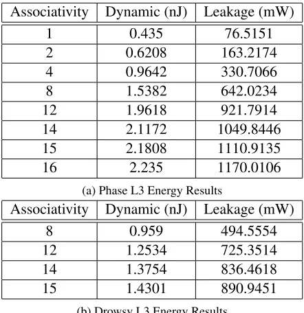
[image:54.612.199.420.88.316.2](b) Drowsy L3 Energy Results
Table 4.11: CACTI L3 Final Energy Results
4.3
Multi2sim
Multi2sim is an application-only simulation framework for heterogeneous computing [20].
This simulator is highly configurable, allowing for multithreaded and multicore
simula-tions. It also has a highly configurable memory hierarchy allowing for simulations with
very customized cache configurations. This simulator has been used and modified to
im-plement the work described here.
Previous work has been done on this simulator as described in [10]. Brendan Fitzgerald
et al. added a new input parameter to turn phase adaptive behaviour on and off for each configurable cache level. Also the simulator was modified to keep track of static and
dy-namic power consumption using the equations and results discussed previously. This was
implemented for L2 only. Variables were also added to keep track of the MRU counters,
accesses, misses, and swaps occurring throughout a simulation. MRU counters are used to
there is a hit in a particular way, that MRU counter is incremented. Based on the current
configuration this MRU counter represents hits in either the A or B partition.
This modified version of Multi2sim 3.2 was used for the work described here. The first
portion of the simulator that needed to be modified was the MRU counters. There was a
bug in the previous modifications that resulted in an incorrect number of hits being recorded
for each MRU state. This just required ensuring the the MRU counters were updated each
and every time there was a hit in a particular cache level. From there, the phase adaptive
implementations for L1 and L3 were added. Care was taken to follow the coding standards
of both the original authors and the previous additions that were made.
These modifications required adding additional control algorithms to the portion of the
code that controls the cache structure, as described in [10]. This section determines the
next cache configuration based on the statistics for the just finished phase. In this case
a phase occurs every 15k instructions, as explained in Chapter 3. From there, it sets the
latency for the B partition and records the energy usage of the previous phase. For L1 and
L3 variables were added to collect the statistical information. Then the configuration costs
are determined using Equation 3.2 and Equation 3.3. Equation 4.1 is also used to convert
the leakage power values to leakage energy.
LeakageEnergy =
LeakageP ower∗CycleCount
3GHz (4.1)
After that step, the next configuration is determined by comparing the energy usage from all
of the possible configurations of the just finished phase. After that is complete the counters
4.3.1 Simulation Configurations
The memory configuration was chosen to match the simulations done by Jorge Albericio
in [2] for comparison. The same base cache sizes and configurations were used for all
sim-ulations. The only modifications were which levels where phase adaptive and which were
not. These cache configurations are shown in Table 4.12. The CPU specific configuration
is shown in Table 4.13.
Parameter Value
General LRU, 64B line, 2 Read ports, 2 Write Ports L1 Cache Split, 32KB, 4 way, 4 cycle
L2 Cache 256KB, 8 way, 5 cycle L3 Cache 8MB, 16 way, 16 cycle
Table 4.12: Memory Configurations for All Simulations
Parameter Value
Fetch Queue 64 bytes
Decode Width 4 instructions
Branch Predictor Combined, 1024 entry BTB, 1024 entry Biomodal, Two level 8K history table
Return Address Stack 16 entry
Issue & Commit Width 4 instructions
Reorder Buffer Size 129
Table 4.13: Processor Configuration
The architecture used for the multicore simulations is shown in Figure 4.9. There are a total
of two cores and four threads running. The configuration for each of the individual cache
levels is kept the same as shown in Table 4.12.
4.3.2 Benchmarks
The SPEC2006 benchmark suite [6] was used for all of the simulations. These benchmarks
are listed in Table 4.14. For the multithreaded and multicore simulations different
Figure 4.9: Multiple Core Configuration [2]
the IPC performance of each of the different benchmarks shown in Table 4.15. The
combi-nations of these benchmarks simulate both mixes of high performance benchmarks as well
as benchmarks with low IPC performance. Mixes are also created based on theMisses Per Kilo Instruction (MPKI) for both cache level 1 (MPKIL1) and level 2 (MPKIL2). Each of these benchmarks will be run for a maximum number of cycles to allow for enough to
occur to show useful results.
4.4
Summary
This chapter outlines the methods used to implement the design outlined in Chapter 3. It
first outlines the previous SPICE simulations done in [10]. From there it describes how
CACTI is used to determine the hardware parameters for energy and latency, as well as
how Multi2sim is modified to simulate this design. The SPEC2006 benchmarks used, as
well as the simulation configurations are also described here. In the next chapter the results
Test Description SPECINT
401.bzip Modified bzip2 to run in memory opposed to I/O 403.gcc Generates code based on GCC version 3.2 456.hmmer Protein sequence analysis using Markov models 459.sjeng An artificial intelligence program that plays chess 462.libquantum Simulates a quantum computer running Shor’s
fac-torization algorithm
471.omnetpp Models a large ethernet network using OMNet++ SPECFP
433.milc Quantum Chromodynamic simulator
434.zeusmp Fluid dynamic simulation of astrophysical phenom-ena
436.cacatusADM Einstein evolution equation solver using staggered leapfrog method
447.dealII Solves a Helmholtz-type equation with non-constant coefficients
450.soplex Linear program simulator using a simplex algorithm and sparse linear algebra
454.calculix Finite element code for linear and nonlinear 3D structures
[image:58.612.134.486.125.458.2]465.tonto Open source quantum chemistry package 470.lbm Simulates incompressible fluids in 3D
Table 4.14: Spec2006 Benchmarks Used [6]
Benchmark IPC MPKIL1 MPKIL2
mcf 0.58 102 5
hmmer 1.19 4 0.001
milc 0.66 19 9
dealII 1.6 4 0.1
lbm 0.43 57 26
[image:58.612.210.410.553.641.2]Chapter 5
Results
The drowsy phase adaptive cache is designed to reduce dynamic energy consumption and
reduce leakage power consumption while incurring a small performance penalty. These
aspects will be shown and analyzed for each cache level implemented for single threaded,
multithreaded, and multicore architectures.
5.1
Experiments
The following experiments, shown in Table 5.1, have been performed for each of the
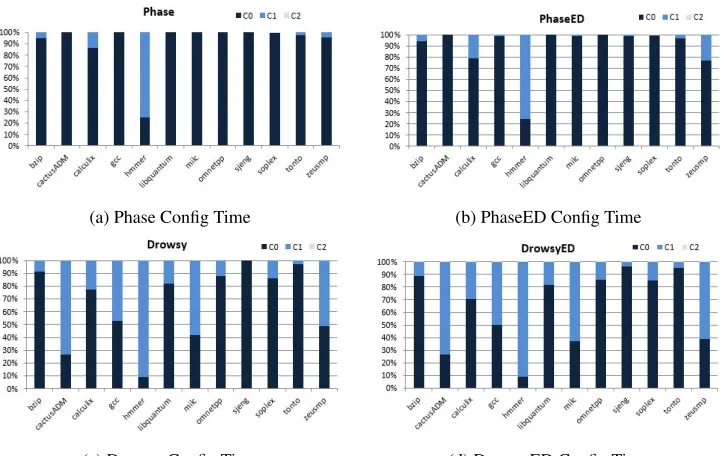
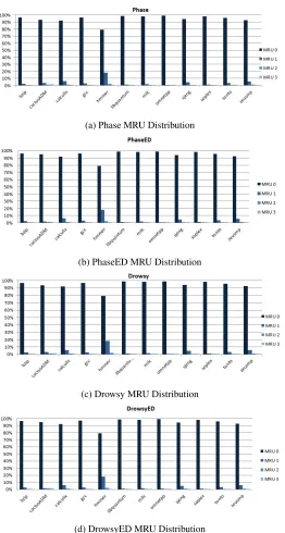
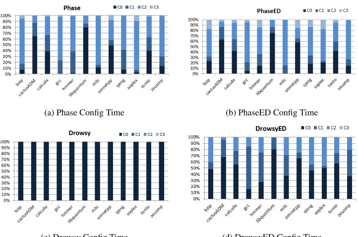
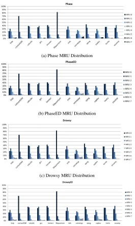
bench-marks shown in Table 4.14 and will be shown in the following figures.
Configuration name Description
Baseline The cache configuration was held unpartitioned Phase The cache configuration is determined on the
MRU statistics, energy and leakage. Drowsy The cache configuration is determined on the
MRU statistics, energy and leakage with the B partition being put into the drowsy state.
PhaseED The cache configuration is determined on the MRU statistics and the energy-delay product.
DrowsyED The cache configuration is determined on the MRU statistics, and the energy-delay product with the
B partition being put into the drowsy state .
5.2
Single Threaded Results
The first set of results gathered is for single threaded simulations. First the simulations are
run with each cache level set to be phase adaptive independently. Finally, a simulation is
run with all three levels active together.
5.2.1 L1 Results
The following set of results are for a cache sys
![Figure 2.1: Hardware Design for a Single Way in a Selective Way Cache [3]](https://thumb-us.123doks.com/thumbv2/123dok_us/42585.3811/19.612.112.510.224.576/figure-hardware-design-single-way-selective-way-cache.webp)
![Figure 2.2: Example Partitioning for 256KB Banks [5]](https://thumb-us.123doks.com/thumbv2/123dok_us/42585.3811/21.612.98.510.89.419/figure-example-partitioning-for-kb-banks.webp)
![Figure 4.9: Multiple Core Configuration [2]](https://thumb-us.123doks.com/thumbv2/123dok_us/42585.3811/57.612.242.379.101.262/figure-multiple-core-conguration.webp)
![Table 4.14: Spec2006 Benchmarks Used [6]](https://thumb-us.123doks.com/thumbv2/123dok_us/42585.3811/58.612.210.410.553.641/table-spec-benchmarks-used.webp)