Int. J. Electrochem. Sci., 7 (2012) 12054 - 12063
International Journal of
ELECTROCHEMICAL
SCIENCE
www.electrochemsci.org
The Design and Simulation of a Planar Microarray Dot
Electrode for a Dielectrophoretic Lab-on-Chip Device
Bashar Yafouz, Nahrizul Adib Kadri*, Fatimah Ibrahim
Medical Informatics and Biological Micro-Electro-Mechanical Systems (MIMEMS) Specialized Laboratory, Department of Biomedical Engineering, Faculty of Engineering, University of Malaya, 50603 Kuala Lumpur, Malaysia
*
E-mail: [email protected]
Received: 1 October 2012 / Accepted: 24 October 2012 / Published: 1 December 2012
Dielectrophoresis (DEP) has been proven as a method of manipulating and analyzing the electrophysiological properties of bioparticles by applying non-uniform electric fields generated through special electrodes. Various electrode geometries have been developed to address different applications. Electric field simulation over electrodes is essential in order to optimize the generated DEP force for cell manipulation. This paper describes the study of electric field distribution over planar multiple microarray dot electrodes using numerical modeling of Comsol Multiphysics 4.2a®. Electric field evaluation for different dot sizes has been demonstrated by applying a range of frequencies to the designed electrodes. Results show that the electric field is axisymmetrical around the center of the dot aperture and that it is higher at the dot edges than the dot centers. Furthermore, adding ground plane between adjacent dots increases the electric field strength.
Keywords: Dielectrophoresis; Numerical modeling; Dot microarray electrodes
1. INTRODUCTION
Microfluidic devices have the potential to be used for early detection and diagnosis of disease at Point-of-Care (POC). This is aligned with the current trend of miniaturizing laboratory equipment to achieve better reactions efficiency, faster results, portability and lower reagents consumption. One of the platforms used in microfluidic devices is Lab-on-chip, which is a potential solution for an automated bio-microfluidic diagnostic system that requires the minimum quantity of blood and offers fast and high-throughput results.
invasiveness and low cost. DEP has been used as a method for cell manipulation and characterization since its discoverer Pohl [1] launched a novel technique for separating living cells from admixed dead ones, taking advantage of the unique electrical properties of each bioparticles [2]. DEP is the phenomenon that describes the motion of polarizable particles through a non-uniform electric field. One of the core strengths of DEP is that the characterization of different cells depends only on the dielectric properties controlled by the particle’s individual phenotype. Hence, the process does not require specific tags or involve chemical reactions [3].
The DEP force depends on the applied frequency and geometry of the electrodes used to generate the electric field. Different electrode geometries have been used in previous studies for different applications. This study provides a numerical analysis of the electric field generated by a 4x4 planar multiple microarray dot electrode, which is a modification of that used by Fatoyinbo et al. [4]. The adjustment geometry parameters for the electrode were employed to produce the optimum design. In order to optimize the size of the dots, the designed electrodes were numerically analyzed and their electric field strength and distribution were compared for different dot diameters. The dots diameter was adjusted by changing either the ring width or the distance between the adjacent dots. Moreover, the effect of adding ground plane between dot apertures was evaluated. These electrodes will be used to conduct DEP expirements as a sample preparation prior to the stage of infectious dieases diagnosis.
1.1. Dielectrophoretic theory
Applying a non-uniform electric field to polarizable particles that are placed in a conductive medium produces DEP force. The magnitude and direction of the DEP force depends on the relative polarizability of the particle and the surrounding medium [5]. The DEP force acting on a spherical particle can by expressed by the following equation [6]:
2 3
)] ( Re[
2 r K E
FDEP o m
(1)
where εo is the permittivity of free space, εm is the permittivity of the surrounding medium, r is the particle radius, ∇E is the electric field gradient and Re[K(ω)] is the real part of Clausius-Mossotti factor, which is defined as:
m p m p K 2 )
( (2)
where ε* is the complex permittivity and subscripts p and m denote particles and medium respectively. Moreover, the complex permittivity ε* is described by:
where ε is the permittivity, j 1, σ is the conductivity and ω is the angular frequency of the
applied AC electric field. The value of Re[K(ω)] for a sphere ranges between -0.5 and 1, and depends on the frequency of the applied AC electric field and relative polarizability between the particle and its surrounding medium [6]. When Re[K(ω)] > 0, the particles undergo positive DEP and move toward the high electric field gradient region. However, when Re[K(ω)] < 0, the particles travel to the low electric field gradient region as a result of the negative DEP effect.
1.2. Electrode design
In order to minimize the value of the applied voltage, the non-uniform electric field required for DEP is typically produced by electrodes on the scale of microns. Electrode geometries can be categorized into two main groups: planar and 3D electrodes. Planar electrodes are typically patterned on the bottom of the microchannel using conventional lithography techniques. Examples of planar electrode designs include interdigitated [7], castellated [8], spiral [9], curved [10], oblique [11], quadrupole [12], matrix [4] and polynomial [13]. On the other hand, 3D electrodes are designed on the bottom, bottom/top, or side wall of the microchannel using complicated techniques. Examples of 3D electrode designs are grid [14], microwells [15], DEP-well [16], extruded [17], sidewall patterned [18] and top-bottom patterned [19]. This variety of electrode geometry has evolved in response to the need to address different research tasks. Hence, the electrode geometry that is used is determined by the general goal of the study.
A planar multiple microarray dot electrode was chosen in this study because it has a well-defined and enclosed region of analysis. This type of electrode has been proven to create electric fields with axisymmetrical gradient around every dot aperture [20]. The current 4x4 microarray dot electrode was designed in this study in such a way that individual dots can be electrically supplied independently, giving the capability to observe and record cellular electrophysiological changes in near real-time by conducting multiple DEP experiments in parallel.
2. METHODOLOGY
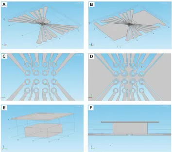
AC/DC module of Comsol Multiphysics 4.2a® (COMSOL Inc, Palo Alto, USA) was used to model the electric field distribution over the microarray dot electrodes. A few assumptions were made to mimic the actual situation and to provide greater processing memory and a better fitting mesh of the model. Two main 3D models were designed in order to perform the objective of the study. These are shown in Fig. 1.
5x5x0.1 mm3 solid block, while the gasket chamber was represented by 3x3x1 mm3 solid block, as depicted in Fig. 1(E) and (F).
Figure 1. Two designs of the planar multiple microarray dot electrode: (A) the full design for electrodes without ground plane between dots apertures. (B) the design with ground plane between dots apertures. The pattern of the 4x4 microarray dot electrode without ground plane (C) and with ground plane (D). (E) three dimensional view of the ground electrode and the gasket chamber, while (F) is a front view of the entire design.
In order to optimize the size of the dots, dots were given diameters of 100, 150, and 200 μm for both electrode designs. The diameter of the dots was adjusted by changing either the ring width or the distance between adjacent dots. First, the size of the dots was modified by varying the ring width 100, 75 and 50 µm, for the diameters of 100, 150, and 200 μm respectively. The distances between adjacent dots and between the center of the dots were fixed at 150 and 450µm respectively. Second, in order to investigate whether the ring width variation has an effect on the electric field strength, other simulations were conducted such that the width of the rings was fixed at 50 µm for all sizes of the dots, while varying the distances between adjacent dots (distance between dots centers remained fixed at 450 µm).
The patterned dot electrode and ground plane between the aperture of the dots were given gold properties σ = 4.1x10⁷
S/m and εr =1, the ground top electrode was given material properties of indium tin oxide (ITO) σ = 1.3x10⁴
[image:4.596.119.473.130.444.2]
suspending medium, was given the material properties of deionized water σ = 2x10⁻⁴ S/m and εr =78 [20, 21].
The entire geometries were meshed using tetrahedral elements with maximum and minimum element sizes of 5 and 0.05mm respectively. Boundary conditions for the top electrode and ground plane between the apertures of the dots were defined as ground, while the patterned electrode was supplied with 10Vp.
A range of frequencies was applied to observe any changes in the generated electric field strength and distribution over the designed electrodes. The applied frequencies were 100 Hz, 1 kHz, 10 kHz, 50 kHz, 100 kHz, 500 kHz, 1 MHz and 2 MHz.
3. RESULTS AND DISCUSSION
Different experiments were conducted utilizing different frequencies; however, the change in the electric field strength (V/m) and distribution was negligible. Frequency plays a significant role in determination of the Clausius-Mosotti factor [K(ω)], which affects the DEP force, as expressed in equation (1) [6]. Therefore, frequency controls the DEP force via Clausius- Mossotti factor rather than electric field strength.
The rest of the experiments were simulated by applying 100 kHz. Fig. 2 shows the distribution of the strength of the electric field of the electrodes without ground plane between the apertures of the dots, with dot diameters 100, 150 and 200 µm. On the other hand, Fig. 3 illustrates the distribution of the electric field strengths of electrodes with ground plane between the apertures of the dots, with dot diameters of 100, 150 and 200 µm. These results are associated with the adjustment of ring width to change the diameters of the dots. The strength of the electric field is illustrated by color ranging from blue (least strength) to red (most strength).
The results revealed that the values of the electric field strength at the edge of the dots are higher than that at the center of the dots for all electrode designs. This is aligned with the previous simulations in the literature that show the electric field of a planar electrodes increases near the electrode edge [6, 22-24]. Therefore, the DEP force is expected to be higher at the dot edges rather than at the dot centers, which is in agreement with the earlier works of Fatoyinbo et al. [4, 20].
Moreover, Fig. 2 and 3 depicts that the electric field strengths are axisymmetrical around the center of the aperture of the dots, which suggests that the DEP force is also axisymmetrical within the dot volume. This indicates that the particles will undergo homogenous radial movement. The direction of this movement will depend on Clausius-Mossotti factor. If it is positive, particles will be attracted to the dot edges. However, if Clausius-Mossotti factor is negative, particles will be repelled to the centers of the dots. This finding is in consistent with the work done by Kadri et al., in which K562 leukemic cells were collected at the centers of the dots in the case of negative DEP, and attracted to the dot edges in the case of positive DEP [25].
et al., the gaps between adjacent electrodes should be wide enough compared to the diffusion layer thickness; in order to prevent the overlapping between the diffusion layers of the adjacent electrodes [26]. Thus, the advantageous outcome of inserting ground plane between adjacent dots in the proposed electrode is due to the fact that the overlapping that might occur between the electric fields generated by adjacent dots is avoided; since the ground plane absorbs any charges in this area.
[image:6.596.157.437.182.702.2][image:7.596.132.461.81.716.2]
Table 1. Maximum electric field strengths (V/m) of electrodes with/without ground plane between dot apertures for different dots diameters.
Dot Diameter (µm) 100 150 200
Electrodes without ground plane between dots
7.057*104 7.423*104 7.914*104 Electrodes with ground plane
between dots
3.426*105 3.194*105 2.885*105
[image:8.596.177.418.224.689.2]
Table 2. Maximum electric field strengths (V/m) of electrodes without ground plane between dot apertures with fixed dots separation distance and with fixed ring width for different dots diameters.
Dot Diameter (µm) 100 150 200
Electrodes with fixed dots separation distance (150 µm)
7.057*104 7.423*104 7.914*104 Electrodes with fixed ring width
(50 µm)
8.731*104 6.372*104 7.914*104
Table 1 shows that the values of electric field strength are decreased when the diameter of the dots in the electrodes are increased with ground plane between dots. The highest electric field strength value is 3.426*105 V/m and this is associated with an electrode that has a dot diameter of 100 µm.
On the other hand, the values of electric field strength are increased as the diameters of the dots in the electrodes are increased when there is no ground plane between dots, as shown in Table 1. The maximum electric field strength was produced by an electrode that had a dot diameter of 200 µm.
Changing dot diameters in the previous electrodes was done by changing the ring width. To explore what effects the ring width may have on the electric field strength and distribution, electrodes with different dot diameters were designed with fixed ring width (50 µm) for all sizes of dots, while varying the distances between the adjacent dots. The results of the electric field strengths of these electrodes are shown in Fig. 4. The results reveal that the distribution of the electric field over the dot electrodes is similar to that shown in Fig. 2. Hence, ring width does not affect electric field distribution.
Table 2 depicts the maximum values of the electric field strengths of electrodes with fixed dots separation distance and electrodes with fixed rings. The findings show that there are insignificant differences between the two cases. Therefore, ring width has no major effect on the induced electric field strength over the dot electrodes.
4. CONCLUSION
ACKNOWLEDGMENT
This research is financially supported by the University of Malaya, Ministry of Higher Education High Impact Research Grant (UM/HIR/MOHE/ENG/05), and University of Malaya Research Grant (UMRG: RG023/09AET)
References
1. H. A. Pohl, J. Applied Physics, 22 (1951) 869 2. H. A. Pohl, I. Hawk, Science, 152 (1966) 647
3. N. A. Kadri, PhD Thesis, University of Surrey, (2011)
4. H. O. Fatoyinbo, N. A. Kadri, D. H. Gould, K. F. Hoettges, F. H. Labeed, Electrophoresis, 32 (2011) 2541
5. R. Pethig, G. H. Markx, Trends in biotechnology, 15 (1997) 426 6. J. Cao, P. Cheng, F. Hong, J. Electrostatics, 66 (2008) 620
7. J. Auerswald, H. F. Knapp, Microelectronic engineering, 67 (2003) 879
8. F. F. Becker, X. B. Wang, Y. Huang, R. Pethig, J. Vykoukal, P. Gascoyne, Proceedings of the National Academy of SciencesI, 92 (1995) 860
9. X. B. Wang, Y. Huang, X. Wang, F. F. Becker, P. Gascoyne, Biophys. J., 72 (1997) 1887
10. K. Khoshmanesh, C. Zhang, F. J. Tovar‐Lopez, S. Nahavandi, S. Baratchi, K. Kalantar‐zadeh, A. Mitchell, Electrophoresis, 30 (2009) 3707
11. M. S. Pommer, Y. Zhang, N. Keerthi, D. Chen, J. A. Thomson, C. D. Meinhart, H. T. Soh, Electrophoresis, 29 (2008) 1213
12. L. S. Jang, P. H. Huang, K. C. Lan, Biosens. Bioelectronics, 24 (2009) 3637 13. M. P. Hughes, H. Morgan, J. Physics D: Applied Physics, 31 (1998) 2205 14. J. Suehiro, R. Pethig, J. Physics D: Applied Physics, 31 (1998) 3298 15. R. S. Thomas, H. Morgan, N. G. Green, Lab Chip, 9 (2009) 1534
16. K. F. Hoettges, Y. Hübner, L. M. Broche, S. L. Ogin, G. E. N. Kass, M. P. Hughes, Anal. Chem., 80 (2008) 2063
17. C. Iliescu, L. Yu, F. E. H. Tay, B. Chen, Sensors and Actuators B: Chemical, 129 (2008) 491 18. L. Wang, J. Lu, S. A. Marchenko, E. S. Monuki, L. A. Flanagan, A. P. Lee, Electrophoresis, 30
(2009) 782
19. M. Dürr, J. Kentsch, T. Müller, T. Schnelle, M. Stelzle, Electrophoresis, 24 (2003) 722 20. H. O. Fatoyinbo, K. F. Hoettges, M. P. Hughes, Electrophoresis, 29 (2008) 3
21. Serway, Raymond, Principles of Physics. 2nd ed.; Saunders College Publishing: Fort Worth, Texas; London, (1998)
22. M. Cha, J. Yoo, J. Lee, Electrochemistry Communications, 13 (2011) 600
23. S. Burgarella, S. Merlo, B. Dell’Anna, G. Zarola, M. Bianchessi, Microelectronic Engineering, 87 (2010) 2124
24. H. Chuang, D. M. Raizen, A. Lamb, N. Dabbish, H. H. Bau, Lab Chip, 11 (2011) 599 25. N. A. Kadri, M. A. Abdul Razak, F. Ibrahim, In. J. Electrochem. Sci., 7 (2012) 5633