epilayers grown by molecular beam epitaxy
C. Bazioti, E. Papadomanolaki, Th. Kehagias, T. Walther, J. Smalc-Koziorowska, E. Pavlidou, Ph. Komninou, Th. Karakostas, E. Iliopoulos, and G. P. Dimitrakopulos
Citation: Journal of Applied Physics 118, 155301 (2015); doi: 10.1063/1.4933276 View online: http://dx.doi.org/10.1063/1.4933276
View Table of Contents: http://scitation.aip.org/content/aip/journal/jap/118/15?ver=pdfcov Published by the AIP Publishing
Articles you may be interested in
Structural anisotropic properties of a-plane GaN epilayers grown on r-plane sapphire by molecular beam epitaxy J. Appl. Phys. 115, 213506 (2014); 10.1063/1.4880957
Highly luminescent, high-indium-content InGaN film with uniform composition and full misfit-strain relaxation Appl. Phys. Lett. 103, 131101 (2013); 10.1063/1.4822122
Defect reduction in GaN/(0001)sapphire films grown by molecular beam epitaxy using nanocolumn intermediate layers
Appl. Phys. Lett. 92, 121902 (2008); 10.1063/1.2899944
Reduction of threading defects in GaN grown on vicinal SiC(0001) by molecular-beam epitaxy Appl. Phys. Lett. 77, 1105 (2000); 10.1063/1.1289266
Optical properties of GaN epilayers and GaN/AlGaN quantum wells grown by molecular beam epitaxy on GaN(0001) single crystal substrate
Defects, strain relaxation, and compositional grading in high indium content
InGaN epilayers grown by molecular beam epitaxy
C.Bazioti,1E.Papadomanolaki,2Th.Kehagias,1T.Walther,3J.Smalc-Koziorowska,4 E.Pavlidou,1Ph.Komninou,1Th.Karakostas,1E.Iliopoulos,2and G. P.Dimitrakopulos1,a)
1
Physics Department, Aristotle University of Thessaloniki, GR 541 24 Thessaloniki, Greece 2
Microelectronics Research Group (MRG), IESL, FORTH, P.O. Box 1385, 71110 Heraklion Crete, Greece and Physics Department, University of Crete, Heraklion Crete, Greece
3
Department of Electronic & Electrical Engineering, University of Sheffield, Sheffield S1 3JD, United Kingdom
4
Institute of High Pressure Physics, Polish Academy of Sciences, Sokolowska 29/37, 01-142 Warsaw, Poland
(Received 7 July 2015; accepted 3 October 2015; published online 16 October 2015)
We investigate the structural properties of a series of high alloy content InGaN epilayers grown by plasma-assisted molecular beam epitaxy, employing the deposition temperature as variable under invariant element fluxes. Using transmission electron microscopy methods, distinct strain relaxa-tion modes were observed, depending on the indium content attained through temperature adjust-ment. At lower indium contents, strain relaxation by V-pit formation dominated, with concurrent formation of an indium-rich interfacial zone. With increasing indium content, this mechanism was gradually substituted by the introduction of a self-formed strained interfacial InGaN layer of lower indium content, as well as multiple intrinsic basal stacking faults and threading dislocations in the rest of the film. We show that this interfacial layer is not chemically abrupt and that major plastic strain relaxation through defect introduction commences upon reaching a critical indium concentra-tion as a result of composiconcentra-tional pulling. Upon further increase of the indium content, this relaxa-tion mode was again gradually succeeded by the increase in the density of misfit dislocarelaxa-tions at the InGaN/GaN interface, leading eventually to the suppression of the strained InGaN layer and basal stacking faults.VC 2015 AIP Publishing LLC. [http://dx.doi.org/10.1063/1.4933276]
I. INTRODUCTION
InxGa1xN epitaxial films with high indium content are
important for optoelectronics applications up to the near-infrared, as well as for high efficiency photovoltaics. The tai-loring of the indium composition, in principle, permits bandgap tunability from 0.7 up to 3.4 eV, thus allowing utili-zation of most part of the solar spectrum.1,2However, due to the immiscibility of alloy constituents, chemically induced phenomena, such as phase separation and compositional pulling, may take place, resulting in complex defect micro-structures that are sensitive to the growth conditions.3–6
The fluctuations in the indium concentration can be either long- or short-range in character. Short-range ones cause the local depletion of indium around regions that exhibit higher InN molar fraction. Elastic strain shifts the center of the misci-bility gap to higher indium contents leading to the appearance of periodic compositional fluctuations.7,8Line and extended defects, such as threading dislocations (TDs), can induce local indium clustering.9–13On the other hand, compositional pull-ing is a mesoscale phenomenon, whereby the compressive strain due to the interfacial misfit impedes incorporation of the larger indium atoms, causing a gradually increasing in-dium concentration with increasing film thickness.14
Plasma-assisted molecular beam epitaxy (PAMBE), in principle, is a suitable growth method for achieving high
(x>0.2) indium contents. It can be employed in order to take advantage of metastability, and to avoid phase separa-tion, by exploiting low growth temperatures (Tgr) so that the mobility of indium atoms is reduced.15Due to the easier dis-sociation of In-N bonds, indium incorporation is favored at
Tgr<500C. 15,16
On the other hand, the surfactant effect of the indium adlayer formed under metal enrichment of the surface favors the desired two-dimensional (2D) growth.17 Iliopoulos et al.18 have demonstrated PAMBE-growth of (0001) InGaN films over the entire composition range with high indium incorporation efficiency, using a low tempera-ture range and almost stoichiometric flux ratios. Phase sepa-ration and a decrease of the indium content along the growth direction have been observed in PAMBE growth at higher temperatures.19,20 Film growth at the indium accumulation limit and at temperatures where InGaN decomposition is active has been reported.21
The defect microstructure of the epilayer, in conjunction with the indium distribution and strain content, is crucial for device efficiency. The microstructure depends in a sensitive manner on the operating mechanisms for misfit relief, which, in turn, are affected by the growth kinetics. The concept of “critical thickness,”hcr, describes the response of the system to the stored elastic energy. The interplay between chemistry and available strain relaxation modes has been pointed out in multiple previous works that concern principally epilayers grown by metalorganic vapor phase epitaxy (MOVPE). Spinodal decomposition was reported in InGaN films with indium content xⲏ0.3.8 V-pit formation from TDs was
a)Author to whom correspondence should be addressed. Electronic mail:
reported as a mechanism of strain relaxation in films with
xⱗ0.15, whereas pyramidal slip through the Matthews-Blakeslee mechanism22 operated when the TD density was significantly reduced.23,24When free surfaces intercepted the epitaxial interface, e.g., due to pits, relaxation proceeded through basal slip of misfit dislocation half-loops.25
Below hcr (according to the People-Bean model),26 the film retains a principally elastic strain state and the composi-tional pulling phenomenon appears.27,28Abovehcr, reciprocal space x-ray diffraction (XRD) maps of asymmetrical reflec-tions often exhibit double points associated with discontinu-ous strain relaxation along the growth direction, and what may also be a chemical discontinuity. Strain discontinuity but no compositional gradient was reported in 120 nm thick In0.19Ga0.81N.29Liliental-Weberet al.30studied In0.28Ga0.72N and In0.40Ga0.60N epilayers using transmission electron mi-croscopy (TEM) and correlated the double points to a self-formed pseudomorphic InGaN interlayer between the main film and the substrate, which was termed a “sequestration layer” (SQL) and had lower indium concentration (0.17 in the first case and 0.23 in the second). Contrary to the SQL, the main epilayer was very rich in basal stacking faults (BSFs). It also exhibited a saw-tooth surface structure. When the indium content was increased to 0.45, the SQL was suppressed but the BSFs and surface roughness persisted. However, in another study, of In0.08Ga0.92N with 30 nm thickness,31 sequestration was observed despite that the thickness was far below critical. One sublayer had a 10 nm thickness and
x¼0.04, whereas the second one had a 25 nm thickness and
x¼0.10. In later work on low (0.10) indium content films, Liliental-Weberet al.28observed that the phenomena of sur-face roughening and BSF introduction became more intense with increasing film thickness, giving rise to polytype-like areas. Choet al.32also observed saw-tooth surface roughening and introduction of multiple BSFs in epilayers with indium content between 0.18 and 0.45. However, although they reported that the InGaN region closer to the GaN substrate retains more elastic strain, they found a gradual and not dis-continuous strain relaxation with increasing thickness, with most relaxation occurring between 20 and 50 nm thickness. In the study of Wanget al.,33sequestration was correlated to dis-location glide on pyramidal planes from the film surface. Pantzas et al.34 employed Z-contrast imaging to view a 140 nm sequestrated In0.2Ga0.8N film and found that the SQL containedx¼0.13 indium. Based on their Z-contrast quantifi-cation, they observed a stark compositional difference between the SQL and film, explained by the absence of com-positional pulling. Wilschet al.35found that indium remained constant atx¼0.13 up to100 nm and this layer was relaxed by 20%. Then, it increased up tox¼0.19 in the next 200 nm and saturated in the relaxed 100 nm thick upper part. M€uller
et al.36 employed atom probe tomography in 300 nm In0.25G0.75N to show that indium remains almost constant in the SQL (40 nm thick) and then starts to increase gradually.
It has been suggested that the strain discontinuity of the SQL should be attributed to a transition from 2D growth to Stranski-Krastanow type 2D/3D growth and that it is invaria-bly associated with the saw-tooth roughening of the film sur-face, which aids the incorporation of indium.37–40 The
sequestration phenomenon has also been observed in PAMBE-grown epilayers, but the relevant reports in films grown by this method are very sparse.21,41
Based on the afore-given literature review, there is no consensus on what actually takes place during the relaxation of InGaN films, i.e., if there is a strain or compositional dis-continuity (or both) close to the InGaN/GaN interface or whether chemical and strain gradients are in place. Also, we do not understand clearly the onset of defect introduction and how critical thickness calculations need to be modified in order to take into account the dominant and distinct strain relaxation mechanism(s) that appear under the employed growth conditions, especially those of PAMBE growth. Elastic strain and indium surface kinetics constitute the pri-mary driving forces for the realization of such phenomena. In this regard, it is important to achieve a deconvolution of the influences of growth conditions on these two factors and to elucidate the chemical and strain gradients taking place.
In our contribution, we focus on TEM observations of PAMBE-grown films deposited at different temperatures under constant fluxes. Hence, we monitor the changes that occur by influencing just one parameter that affects the dium mobility. We report on the correlation between the in-dium content (on average as well as along the growth direction) and the dominant strain relaxation mechanisms of the films. We demonstrate the change of relaxation mode with temperature and the gradual suppression of the SQL. We also analyze the line and extended defects that are intro-duced, and we elucidate the structure of the sequestration interface. Finally, we report on the correlation between strain relaxation and chemistry, and show that the chemical varia-tion is gradual in the film but the strain variavaria-tion is discontin-uous. Based on our results, we propose that accomplishing early strain relaxation through indium saturation of the growth front is a prerequisite for suppressing the SQL.
II. EXPERIMENT
TEM thin foil preparation for cross sectional observations along the [1120] and [1100] zone axes was performed by me-chanical grinding using the tripod wedge polishing method in the Allied Multiprep, followed by15 min of Arþion milling in the Gatan PIPS. Cross sectional TEM (XTEM), plan view TEM (PV-TEM), and high resolution TEM (HRTEM) obser-vations were performed using a 200 kV JEOL JEM 2011 microscope (point resolution 0.19 nm, Cs¼0.4 mm). High angle annular dark field (HAADF) observations for Z-contrast imaging were performed in a 200 kV FEI TECNAI G2 F20 S-TWIN scanning TEM (STEM). Energy dispersive x-ray spectroscopy (EDX) was performed using a 200 kV JEOL JEM 2010F microscope. Measurements of lattice constant variations at the nanoscale were obtained from HRTEM observations using geometrical phase analysis (GPA).42 For GPA, negatives were digitized at 4000 dpi using a Nikon Super CoolScan 9000ED scanner. The sample surfaces were assessed by scanning electron microscopy using a JEOL JSM6390 LV microscope. High resolution XRD was per-formed using a Bede D1 diffractometer for the determination of the indium and strain content in the samples.
III. RESULTS
A. Average film properties, dislocation densities, and surface morphology
We have considered five samples grown at different temperatures that are listed in Table I. RHEED patterns remained streaky during growth in all samples, indicative of two-dimensional growth. There were no significant observ-able variations in the RHEED patterns during growth, except for sample E, for which the pattern gradually became less streaky, indicative of some surface roughening. TableIlists the average indium contents of the samples, as determined from lattice constant measurements using XRD and selected area electron diffraction (SAED). For the high resolution XRD measurements, the symmetric (0002) and asymmetric
ð1015ÞBragg reflections were employed forc andalattice constant determination, respectively. SAED patterns were recorded along both the [1120] and [1100] zone axes, and results were averaged from at least three sample areas. For both methods, the indium concentration was then extracted by postulating that the epilayers abide to the condition of biaxial residual stress (the so-called “tetragonal distortion”). We also assumed that Vegard’s law is valid, and performed this calculation in the manner described by Moraleset al.,43
using the GaN and InN lattice and elastic constants given therein. The lattice constants of InGaN were measured with reference to those of GaN. The InGaN elastic constants, as functions of the indium content, were obtained by linear interpolation from the respective constants of GaN and InN. Good agreement between SAED and XRD measurements was found, as can be seen in Table I. Furthermore, in all cases, the SAED patterns revealed a good heteroepitaxial relationship between epilayer and substrate, and no second-ary phases.
A decrease of the indium content with increasingTgrwas recorded from the lattice constant measurements, which was attributed to indium desorption and InGaN decomposition. This trend was also reflected in the decrease, with increasing
Tgr, of the film thickness,h, as determined by TEM and listed in Table I. Only sample A did not appear to abide to this trend, having a greater thickness than sample B, and the rea-son for this will be discussed in SectionIII B.
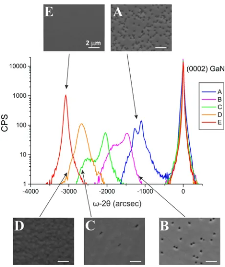
[image:4.612.323.553.468.741.2]We have also listed in TableIthe in-plane total misfitF, and the relaxation parameter R, defined asf/F, wherefis the plastically relaxed strain. Since the films comprised different indium contents,Ris a useful comparative measure of the per-centage of plastic strain relaxation. Significant relaxation (R70%) was observed at x0.18, whereas when indium exceeded 0.35, the films were almost fully relaxed (R>85%). Regarding the structural quality of the films, Fig. 1 depicts XRD (0002) x-2h scans for all the samples. We observe that sample A exhibits clear phase separation with two distinct peaks. For samples B and C, we observe a grad-ing of the (0002) lattice constant with formation of a shoulder-like region on the left hand side of the distributions. This could be attributed either to phase separation by compo-sitional pulling or to strain relaxation following an initial
TABLE I. List of samples grown by varying the growth temperature (Tgr),
including average measurements of indium content (xIn), film thickness (h),
total misfit (F), and strain relaxation (R).
A B C D E
Tgr(C) 590 580 565 535 475
xInby XRD (60.01) 0.12 0.18 0.27 0.36 0.42
xInby SAED (60.01) 0.11 0.17 0.26 0.38 0.41
h(62 nm) 282 200 318 372 445
F(%) 1.23 1.87 2.81 3.98 4.32
R(65%) 39 70 73 90 86 FIG. 1. High resolution XRDx-2hscans of the five samples around the
[image:4.612.50.302.671.765.2]high quality and low-indium content region that corresponds to the sharper peak on the right hand side of each angular distribution. This grading is reduced in sample D and disap-pears altogether in sample E. Elucidation of these findings requires structural observations using TEM and is under-taken in SectionIII B. Figure1also illustrates representative SEM images, given as insets, that depict the surface mor-phologies of the samples. It can be seen that the higher tem-perature sample A exhibited surface pits. These pits were significantly reduced in samples B and C and disappeared al-together in samples D and E. The pit density was reduced from 2108cm2in sample A, to 2.5107cm2in B and 3.8106cm2in C.
Figure 2 gives the (0002) rocking curve FWHM obtained by XRD, in correlation with the density of TDs withc-type [0001] Burgers vector components as determined by TEM. The lowest values were obtained for samples A and E withx¼0.11 and 0.41, respectively, showing better crystal quality. It is noted that Burgers vector analysis by TEM using theg.binvisibility criterion showed that the TDs with a-type 1/3h1120i Burgers vector components were about three times more than those withc-type components.
Overall, the aforegiven comparative study of the films points to sample E as having the lowest defect density and better crystal quality. Detailed structural observations by TEM, given in SectionIII B, elucidate the strain relaxation processes taking place in correlation with the microstructure and the indium content of the films.
B. Defect microstructures
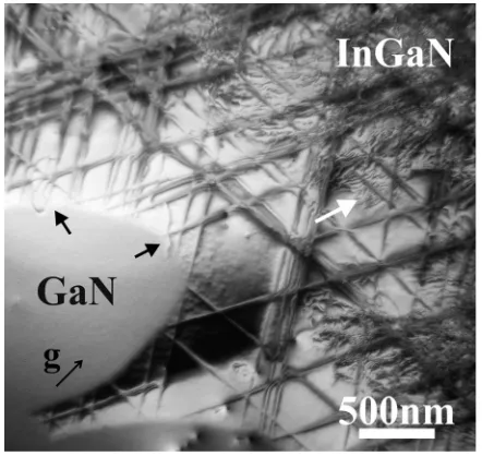
Following an order of decreasingTgrin our presentation of the samples, the structure of the high temperature sample A is shown in the weak beam dark field (WBDF) XTEM images of Figs.3(a)and3(b). As can be seen in the image of Fig.3(a), obtained withg0002, the pits on the sample surface (observed by SEM in Fig. 1) were V-pits associated with ascending TDs withc-type Burgers vector components that propagated from the GaN template. In fact, the V-pit density was almost the same as the TD density in the GaN substrate, i.e., almost all V-pits resulted from TDs coming from the substrate. The V-pits were deep, reaching close to the InGaN/GaN interface. Their surrounding film regions were decorated with a-type TD bundles, as can be seen in Fig. 3(b)obtained with g1100. On the contrary, the rest of the
film exhibited low defect density. There were no regular mis-fit dislocation arrays, but we did observea-type dislocations running parallel to the interface that contribute to the partial misfit relief. Such misfit dislocations may have nucleated at the V-pit areas.23There were several horizontal dislocations along the film height, which were connected to the TD bun-dles at the areas of the V-pits.
The localized defect formation at the V-pits of sample A can be attributed to the larger indium content there, com-pared to the rest of the film, leading to increased local strain. Indium adsorbs preferentially and is incorporated at the cores of the c-type TDs and at the {1101} side facets of the V-pits.44,45 Furthermore, the increased thickness of sample A, which was pointed out in Section III A, could be attrib-uted to this preferential adsorption so that the growth rate for the rest of the film was closer to that of GaN. Another reason for the faster growth is the bunching of surface steps at the V-pits. The opening up of the V-pits started soon after the onset of InGaN growth, but further widening could also be attributed to the InGaN decomposition.
[image:5.612.323.553.61.305.2]The indium distribution in sample A was examined using Z-contrast STEM imaging, as shown in Fig.3(c). Regions of brighter contrast were observed at the facets of V-pits (as indi-cated by arrows), confirming the aforementioned indium seg-regation at these regions. However, what was striking is the appearance of a 50–60 nm thick interfacial zone of abrupt brighter contrast, corresponding to higher indium content close to the heteroepitaxial interface. In order to determine the indium content inside this interfacial zone, we employed measurements of lattice constants from HRTEM images (not shown) using GPA. These measurements yielded an indium
FIG. 2. Graphs of XRD (0002) rocking curve FWHM andc-component TD density versus the growth temperatureTgr.
[image:5.612.57.289.614.741.2]concentration ofx¼0.14, which is higher than the x¼0.12 found in the main film. This difference is consistent with the double XRD peaks shown in Fig.1and was further verified by EDX measurements on the same TEM foils.
Moving to sample B, we found that decreasing the growth temperature by 10C resulted in a drastic change of the strain relaxation mechanism, concurrent with the increase of the in-dium content by 0.06–0.07. As illustrated in Fig.4, the promi-nent structural features of sample B were (a) the appearance of a SQL with low defect density and with average thickness of 40 nm and (b) the introduction of multiple BSFs immediately after this layer, similar to previous literature reports discussed in Sec.I. Contrary to the MOVPE layers, the film surface in our case was almost perfectly flat, and the sequestration phe-nomenon was not associated with a 3D growth mode. Figures 4(a)and4(b)depict bright field (BF) XTEM images, obtained usingg0002 andg1100, respectively. It is seen that TDs were principally ofa-type. Their density (as determined from PV-TEM observations) was equal to 1.31011cm2. Dislocations were also observed inside the GaN substrate, running parallel
to the interface, as shown in Figs.4(b)and4(c). Such substrate dislocations have been reported previously in 200 nm thick In0.12Ga0.88N grown by MOVPE46 and could be related to strain partitioning between the film and the top substrate region. Regarding TDs with c-type Burgers vector compo-nents, new such defects were generated from the s-InGaN/ GaN and InGaN/s-InGaN interfaces (whereby s-InGaN indi-cates the elastically strained InGaN in the SQL), as is visible in Fig.4(a)and is attested by the dislocation density measure-ments in Fig. 2. However, the opening up of such TDs to V-pits was drastically reduced due to the lowering ofTgr.
Misfit dislocations were detected at the s-InGaN/GaN interface of sample B as illustrated in Fig. 4(c). This shows that the SQL was not fully elastically strained but partially relaxed. The misfit dislocations are projected inclined in Fig. 4(c) (arrowed) due to the two-beam imaging condition and thus become well visible. In order to elucidate their character, further observations were undertaken using PV-TEM, and Fig. 5 illustrates such an image from sample B. Three arrays of straight edge-type misfit dislocations aligned along the crystal-lographically equivalent h1100i directions were observed, revealing the operation of pyramidal slip systems during the formation of the SQL,47 and thus confirming the postulate made by Wang et al.33 On occasion, dissociations of these misfit dislocations were observed, as illustrated by black arrows in Fig.5, showing that they may also bear 2aBurgers vector components.47The average spacing of the misfit dislo-cations in sample B was determined atp¼292 nm. Using the equation f¼ b/p, where bis the magnitude of the Burgers vector, the plastic strain relaxation of the SQL was found equal to 0.11% corresponding to a lattice constant of
a¼0.3192 nm for s-InGaN. In order to ascertain the indium content in the SQL of sample B, we also measured the c -lat-tice constant from cross sectional HRTEM observations using
[image:6.612.70.279.332.691.2]FIG. 4. (a) and (b) XTEM two-beam BF images of the same region of sam-ple B, obtained near the [1120] zone axis withg0002 andg1100 conditions, showing TDs withc- anda-type Burgers vector components, respectively. Multiple BSFs are visible inside the InGaN film. The SQL, comprising elas-tically strained InGaN (s-InGaN), is clearly visible in (b). (c) Higher magni-fication from another film area showing the misfit dislocations at the s-InGaN/GaN interface (arrowed).
[image:6.612.328.549.494.703.2]GPA, which gave a value ofc¼0.5317 nm (i.e., 2.5% larger than GaN). Then, the biaxial stress approximation yielded a value ofx¼0.16 for the average indium content in the SQL, i.e., slightly smaller than the average value ofx¼0.18 for the whole film. It is worth pointing out that, for the given indium content of 0.16, the misfit dislocation spacing that is required for complete misfit relaxation is 21 nm, which is lower by one order of magnitude compared to the observed one. In the SQL of sample B, the elastic strain was1.69%, and the relaxation parameter was R¼6%. Compared to the average value of
R¼70% for the whole film B, this shows that the SQL was almost fully elastically strained, and plastic strain relaxation principally commenced above it.
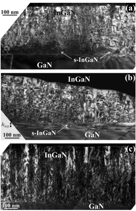
Samples C and D also exhibited a SQL. However, its thickness was found to be reduced to30 nm on average in sample C, as shown in Fig.6(a). This took place through the gradual introduction of more BSFs closer to the InGaN/GaN interface. The SQL of sample D had a similar average thick-ness to that of sample C, despite its much higher indium con-tent. However, the InGaN/s-InGaN interface was now more continuous and well-defined, as illustrated in Fig.6(b). The SQL was fully eliminated in sample E, as shown in Fig.6(c). The SQL of sample D is illustrated in greater detail in the HRTEM image of Fig. 7(a). It can be seen that the InGaN/s-InGaN interface was a principal source of ascend-ing TD half loops, revealascend-ing major plastic accommodation of elastic strain there. In all samples, the InGaN/s-InGaN inter-face was marked by an extended BSF that was discontinuous and stepped. Its character was determined by HRTEM/GPA and was found to be of I1 type as shown in Fig. 7(b). The multiple BSFs that were introduced after this interface were also of I1type in their majority. Their distribution was inho-mogeneous along the height and length of the film. More a-type TDs were found to be introduced from the steps and folds between these BSFs. Since the dominant BSF type is I1, their emanation mechanism is not consistent with that proposed by Meng et al.,48 which requires dissociation of Shockley partial dislocations and hence the existence of I2 BSFs. The TD half loops emanating from the SQL interface and BSFs give rise to the curved dislocation segment con-trast in plan-view observations, as indicated by the white arrow in the thicker parts of the TEM foil in Fig.5.
As mentioned, in the low temperature sample E, the SQL was fully eliminated, and Fig. 7(c) is a characteristic HRTEM image of the InGaN/GaN interfacial region. Detailed structural observations revealed misfit dislocations at the InGaN/GaN interface, but no ordered dislocation array. In addition to the elimination of the SQL, BSFs were also eliminated almost completely in sample E, as can be seen in Figs.6(c)and7(c).
Regarding the transition from SQL to “no-SQL,” our observations indicate that, with increasing indium content, the SQL gradually became decorated witha-type TDs. Such TDs were either introduced directly from the s-InGaN/GaN interface or from inside the SQL, as can be seen by compar-ing Figs.4(b)and6(a). Hence, it appears that the SQL/BSF mechanism was gradually overtaken by the introduction of more misfit dislocations at the s-InGaN/GaN interface, caus-ing more plastic relaxation of the SQL. This leads us to
consider that for a certain combination between strain and chemistry, there is a critical thickness for BSF introduction, relating to the accumulation of a critical amount of indium at the growth front. We address this issue in Section III C by combined GPA and EDX analysis.
C. Compositional and strain profiling of sequestrated samples
As discussed in Sec. I, there has been a debate on whether the SQL is a rather chemically abrupt layer or if its composition varies gradually. Our Z-contrast imaging showed a darker contrast for the SQL compared to the rest of the film, similar to the observation of Pantzas et al.,34 as illustrated in Figs.8(a)and8(b)for samples B and D, respec-tively. However, the brighter contrast above the SQL could signify not only a higher indium content but may also be attributed to the cores of the TDs that give rise to diffuse scattering, i.e., the high TD density could contribute to con-trast formation even at high electron collection angles.49,50 Similarly, the brighter s-InGaN/GaN interfacial contrast could be either due to the chemistry or associated with the misfit dislocations.
Therefore, we have employed EDX profiling in order to ascertain the average indium distribution along the growth
[image:7.612.329.547.59.397.2]direction, without attempting a direct correlation with the Z-contrast images. Figures8(c) and8(d) illustrate EDX files along [0001] for samples B and D, respectively. The pro-files have been obtained from 2D x-ray maps for the respective lines, after averaging for80 nm parallel to the interface. The maps were recorded with a2 nm spot size. What we can see for sample B (x¼0.18) is an initial interfacial region, roughly
20 nm thick (region I) of rather abrupt change of the stoichi-ometry, followed by a more slowly graded region that extends
for40 nm (region II). In other words, the chemical content is graded inside the SQL layer and stabilizes above it. A corre-sponding gradual strain increase was not detected here by HRTEM/GPA, probably because of the very small overall compositional change of 0.02.
Sample D (x¼0.36) also exhibited two compositionally graded regions. The interfacial one (region I) was 10 nm wide, followed by a second region (region II), roughly40 nm wide, having a smaller compositional gradient before the film reached a steady-state indium concentration. It is noted here that some artificial broadening in the delineation of the interfa-cial region is unavoidable due to the influence of the excitation volume, despite the small probe size used. In any case, a real compositional sequestration in the form of chemical disconti-nuity does not seem to exist. Moreover, in sample D, the over-all film thickness that exhibited compositional grading exceeded by almost two times the thickness of the visible SQL [Fig.8(b)], contrary to the case of sample B where these nesses were rather close. This signifies that the critical thick-ness for the onset of BSF formation was reached before the end of the compositional pulling phenomenon in sample D.
Hence, BSF formation should be associated with a criti-cal indium content and the resulting biaxial stress. In sample B, appearance of BSFs commenced when the indium content reached its final value close to 0.2. In order to ascertain if a similar indium content is associated with BSF introduction also in sample D, we undertook a detailed strain analysis of the first 40 nm of epilayer thickness from HRTEM images using GPA. Figure 9 illustrates such a region with corre-sponding GPA for theg1100 andg0002 spatial frequencies, depicting the reduced relative variations of the in-plane and out-of-plane InGaN lattice parameters with respect to that of GaN (expressed as “lattice strain”,elt). The GPA maps were collected using Gaussian masks placed around the respective spatial frequencies. The employed mask size was g/6, i.e., the spatial resolution was 1.6 nm forg0002 and 1.7 nm forg
FIG. 7. (a) Cross sectional HRTEM image along [1120] showing emanation of TD half loops (white arrows) from the InGaN/s-InGaN interface (black arrow) in sample D. (b) HRTEM image with correspondingg1100 phase map and phase profile across the InGaN/s-InGaN interface, obtained with
0.5 nm spatial resolution. The phase change along the growth direction is given as inset. The [0001] growth direction is indicated in all images. (c) HRTEM image along [1120] of the interfacial region of sample E showing emanating TD half-loops from a rather distorted InGaN/GaN interface, and lack of BSFs in the InGaN film.
[image:8.612.65.283.53.542.2] [image:8.612.316.556.63.275.2]1100. It can be seen that thec-lattice constant of the InGaN epilayer acquired almost abruptly the value of 2.2% greater than that of GaN. However, thea-lattice constant increased in a gradual manner, starting from 0.7% at the heteroepitax-ial interface, and reached 2.0%, compared to that of GaN, just above the SQL. Assuming a biaxial stress state, this behavior is justified by a gradual increase of the indium con-tent, starting from 0.16 at the interface and reaching 0.21 at the SQL discontinuity. This shows that BSF formation again commenced at a critical indium concentration of 0.2, in agreement with sample B.
IV. DISCUSSION AND CONCLUSIONS
In the present work, we have focused on the observation of the strain relaxation mechanisms taking place during PAMBE growth while varying only the growth temperature under nominally slightly metal rich conditions. Prominent structural features were identified, and special emphasis was placed on the SQL, in correlation with the chemical distribu-tion and defect introducdistribu-tion.
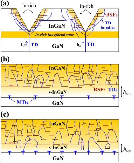
We found that, due to the strain relaxation through V-pit formation at higherTgr, an indium rich interfacial zone was promoted in sample A. Although the observed indium
configuration is reminiscent of that reported by Park et al.51
for MOVPE-grown pyramidal InGaN (whereby the base region of the pyramids exhibited 0.89 indium content com-pared to 0.32 at the rest), in their case such regions were asso-ciated with the influence of ascending TDs. Here, we observed a laterally continuous indium-rich zone, and also its indium content was close to that of the epilayer. We postulate that the thickness of this interfacial zone actually reveals thehcrfor the opening up of the V-pits, since, up to that time, indium was incorporated homogeneously in the film. However, after for-mation of the V-pits, indium was incorporated preferentially there, hence the local introduction of TD bundles, as illustrated schematically in Fig. 10(a). Therefore, we may describe this growth as a modified Stranski-Krastanow mechanism, whereby an initial layer of higher indium concentration formed first. The interplay with the introduction of V-pits defined the sec-ond stage of the growth. We did not observe a strain-induced 3D growth mode since strain relaxation was accomplished through the opening up of TD cores, followed by preferential indium accumulation at these regions. The preferential indium segregation at the V-pits was probably the cause for the reduc-tion of the indium content in the rest of the film.
This situation was reversed at lower growth temperatures, when the indium-deficient sequestration layer appeared, and
[image:9.612.53.386.63.466.2]V-pits gradually disappeared (samples B, C, and D). Contrary to previous reports on MOVPE-grown epilayers,28,30,32,37–40 in our case (PAMBE), the sequestration phenomenon was not correlated to 3D growth. Hence, we do not support the argu-ment that this phenomenon is a manifestation of a Stranski-Krastanow growth mode. This casts doubt on calculations showing that, up to the indium composition of 0.27, the criti-cal thickness for 3D growth is smaller than that for dislocation generation through the Matthews-Blakeslee mechanism.52In our case, we observed partial relaxation even of the SQL through introduction of misfit dislocations, and our plan view observations (Fig.5) indicate the operation of pyramidal slip planes.
Monitoring of the indium gradient along the growth direction of the films did not reveal a direct correlation between this gradient and the SQL thickness. After an initial steep rise, the indium content followed a gradual increase and saturated well below the final film thickness. The SQL was principally elastically strained, and the value of the in-plane strain inside the SQL was also graded. However, most of the elastic strain was plastically relieved at the SQL inter-face. In two representative studied samples, the SQL termi-nated when the indium content reached0.2. This critical indium content corresponded to an accumulated elastic strain energy that triggered the formation of multiple BSFs and associated partial dislocations that contributed to the strain
relaxation process along the height of the film.53 Thus, the SQL interface represented a discontinuity in the strain distri-bution along the growth direction, marking the boundary for the onset of plastic strain relaxation. However, our results did not confirm the claim of other authors that the SQL inter-face is a chemical interinter-face between regions of low and high indium content.34,36Our observations regarding the SQL are summarized in Figs. 10(b)and10(c). It is seen that at inter-mediate indium contents, the SQL is principally elastically strained since the critical indium content for BSF introduc-tion is attained at an average thicknesshcr¼hSQL. Upon fur-ther increase of indium, hSQL is reduced since the critical indium content is attained earlier. However, at the same time, more misfit dislocations are introduced early on. Hence, TD introduction also commences from the heteroepi-taxial interface. At high indium contents, the plastic strain relaxation takes place almost fully at the InGaN/GaN inter-face and so there is no SQL and almost no BSFs.
The easy formation of I1BSFs is consistent with the low energy of this defect compared to the other stacking fault types.54 However, their systematic formation cannot be explained on the basis of energetical considerations alone, but should be justified by the growth kinetics, i.e., the SQL probably has a kinetically defined critical thickness that is dependent on the combination ofTgrand elemental fluxes. In this respect, further experimental studies are required in order to clarify the influence of indium content (and hence strain) variation under constantTgr, i.e., through variation of the fluxes. Based on the present results, we postulate that BSF formation is attributed to partial indium segregation to the growth front, leading to the formation of vacancy islands in the adlayer coverage.55 Such islands accommodate extra indium atoms at their perimeter. The introduction of I1BSFs upon further growth probably also reduces the surface energy. Although explicit studies to this effect are not avail-able to our knowledge, recent calculations by Duff et al.56
show that indium surface atoms release strain energy by relaxing outwards, which may further promote BSF forma-tion due to the small increase in the lattice parameter by the local transition from wurtzite to sphalerite structural units.57
[image:10.612.59.293.63.347.2]By loweringTgrunder invariant fluxes, the thickness of the SQL was reduced as a result, in our opinion, of the earlier accumulation of the critical indium content. Concurrently, the SQL became more relaxed through the introduction of misfit dislocations at the heteroepitaxial interface. We postu-late that, as the initial interfacial concentration of indium approaches the critical value, more misfit dislocations are generated there. Eventually, when this concentration is equal or greater than critical, the sequestration phenomenon is fully suppressed. Hence, the SQL suppression is correlated to the reduced indium desorption and early formation of an indium-rich surface adlayer. This is consistent with the ob-servation of Liliental-Weber et al.30 but, contrary to the MOVPE case, here BSF formation was also suppressed and 2D growth was maintained. The absence of BSFs in our sam-ple E is intriguing, since, in fact, stacking errors should be favored at low Tgr. Therefore, it appears that not only the mobility of indium but also strain is relevant for the appear-ance of the BSFs. In the case of sample E, defect
introduction takes place early on at the heteroepitaxial inter-face, and then a steady state is maintained throughout the rest of the growth.
In summary, we have observed V-pit formation only at samples with lower indium contents and have associated this with a modified Stranski-Krastanow mechanism that can lead to slightly increased indium concentration in the first
50 nm of film thickness. On the other hand, the sequestra-tion phenomenon was observed under 2D growth, contrary to the MOVPE case. In PAMBE-grown films that exhibited sequestration, the chemical concentration along the film thickness saturated gradually, but was not in correspondence with the SQL thickness. The InGaN inside the SQL was par-tially elastically strained, depending on the amount of plastic relaxation that took place through misfit dislocations at the heteroepitaxial interface. This elastic strain increased from bottom to top of the SQL. The coupling between composi-tional pulling and strain relaxation resulted in the introduc-tion of the SQL interface. This interface marks the onset of extensive plastic strain relaxation. The SQL thickness and in-dium content are kinetically defined depending on the perti-nent growth conditions. Suppression of sequestration was achieved through early formation of an indium-rich adlayer.
ACKNOWLEDGMENTS
This research has been co-financed by the European Union (European Social Fund—ESF) and Greek national funds through the Operational Program “Education and Lifelong Learning” of the National Strategic Reference
Framework (NSRF)—Research Funding Program:
THALES, project NITPHOTO. J. S.-K. acknowledges support in the framework of Project BRIDGE: “Elimination of structural defects in nitride semiconductor layers (InGaN and InAlGaN) used as active layers in semiconductor lasers” funded by the Foundation for Polish Science in the frame of the EU operating program Innovative Economy.
1O. Jani, I. Ferguson, C. Honsberg, and S. Kurtz, Appl. Phys. Lett.
91, 132117 (2007).
2C. J. Neufeld, N. G. Toledo, S. C. Cruz, M. Iza, S. P. Den Baars, and U. K.
Mishra,Appl. Phys. Lett.93, 143502 (2008).
3I.-H. Ho and G. B. Stringfellow,Appl. Phys. Lett.69, 2701 (1996). 4D. Doppalapudi, S. N. Basu, K. F. Ludwig, and T. D. Moustakas,J. Appl.
Phys.84, 1389 (1998).
5P. Ruterana and F. Deniel,Mater. Sci. Eng., B59, 186 (1999). 6
F. A. Ponce, S. Srinivasan, A. Bell, L. Geng, R. Liu, M. Stevens, J. Cai, H. Omiya, H. Marui, and S. Tanaka,Phys. Status Solidi B240, 273 (2003).
7T. P. Bartel, P. Specht, J. C. Ho, and C. Kisielowski, Philos. Mag.
87, 1983 (2007).
8N. El-Masry, E. L. Piner, S. X. Liu, and S. M. Bedair,Appl. Phys. Lett.
72, 40 (1998).
9H. K. Cho, J. Y. Lee, C. S. Kim, G. M. Yang, N. Sharma, and C.
Humphreys,J. Cryst. Growth231, 466 (2001).
10H. K. Cho, J. Y. Lee, and J. Y. Leem,Appl. Surf. Sci.221, 288 (2004). 11M. C. Johnson, Z. Liliental-Weber, D. N. Zakharov, D. E. McCready, R. J.
Jorgenson, J. Wu, W. Shan, and E. D. Bourret-Courchesne,J. Electron. Mater.34, 605 (2005).
12
D. I. Florescu, S. M. Ting, J. C. Ramer, D. S. Lee, V. N. Merai, A. Parkeh, D. Lu, E. A. Armour, and L. Chernyak,Appl. Phys. Lett.83, 33 (2003).
13
H. Lei, J. Chen, and P. Ruterana,J. Appl. Phys.108, 103503 (2010).
14
K. Hiramatsu, Y. Kawaguchi, M. Shimizu, N. Sawaki, T. Zheleva, R. F. Davis, H. Tsuda, W. Taki, N. Kuwano, and K. Oki, MRS Internet J. Nitride Semicond. Res.2, e6 (1997).
15Z. Gacˇevic´, V. J. G omez, N. G. Lepetit, P. E. D. Soto Rodrıguez, A.
Bengoechea, S. Fernandez-Garrido, R. N€otzel, and E. Calleja,J. Cryst. Growth364, 123 (2013).
16M. Siekacz, M. Sawicka, H. Turski, G. Cywinski, A. Khachapuridze, P.
Perlin, T. Suski, M. Boc´kowski, J. Smalc-Koziorowska, M. Krysko, R. Kudrawiec, M. Syperek, J. Misiewicz, Z. Wasilewski, S. Porowski, and C. Skierbiszewski,J. Apl. Phys.110, 063110 (2011).
17
E. Monroy, B. Daudin, E. Bellet-Amalric, N. Gogneau, D. Jalabert, F. Enjalbert, J. Brault, J. Barjon, and L. S. Dang,J. Appl. Phys.93, 1550 (2003).
18
E. Iliopoulos, A. Georgakilas, E. Dimakis, A. Adikimenakis, K. Tsagaraki, M. Androulidaki, and N. T. Pelekanos, Phys. Status Solidi A203, 102 (2006).
19
K. G. Belyaev, M. V. Rakhlin, V. N. Jmerik, A. M. Mizerov, Y. V. Kuznetsova, M. V. Zamoryanskaya, S. V. Ivanov, and A. A. Toropov,
Phys. Status Solidi C10, 527 (2013).
20
T. B€ottcher, S. Einfeldt, V. Kirchner, S. Figge, H. Heinke, D. Hommel, H. Selke, and P. L. Ryder,Appl. Phys. Lett.73, 3232 (1998).
21S. Valdueza-Felip, E. Bellet-Amalric, A. Nu~nez-Cascajero, Y. Wang,
M.-P. Chauvat, P. Ruterana, S. Pouget, K. Loren, E. Alves, and E. Monroy,J. Appl. Phys.116, 233504 (2014).
22J. W. Matthews and A. E. Blakeslee,J. Cryst. Growth27, 118 (1974). 23
B. Jahnen, M. Albrecht, W. Dorsch, S. Christiansen, H. P. Strunk, D. Hanser, and R. F. Davis,MRS Internet J. Nitride Semicond. Res.3, e39 (1998).
24
S. Srinivasan, L. Geng, R. Liu, F. A. Ponce, Y. Narukawa, and S. Tanaka,
Appl. Phys. Lett.83, 5187 (2003).
25R. Liu, J. Mei, S. Srinivasan, F. A. Ponce, H. Omiya, Y. Narukawa, and T.
Mukai,Appl. Phys. Lett.89, 201911 (2006).
26
R. People and J. C. Bean,Appl. Phys. Lett.47, 322 (1985).
27S. Pereira, M. R. Correia, E. Pereira, K. P. O’Donnell, C. Trager-Cowan,
F. Sweeney, and E. Alves,Phys. Rev. B64, 205311 (2001).
28
Z. Liliental-Weber, K. M. Yu, M. Hawkridge, S. Bedair, A. E. Berman, A. Emara, J. Domagala, D. R. Khanal, J. Wu, and J. Bak-Misiuk,Phys. Status Solidi C6, 2626 (2009).
29
S. Pereira, M. R. Correia, E. Pereira, C. Trager-Cowan, F. Sweeney, K. P. O’Donnell, E. Alves, N. Franco, and A. D. Sequeira,Appl. Phys. Lett.81, 1207 (2002).
30
Z. Liliental-Weber, M. Benamara, J. Washburn, J. Z. Domagala, J. Bak-Misiuk, E. L. Piner, J. C. Roberts, and S. M. Bedair,J. Electron. Mater. 30, 439 (2001).
31
K. S. Ramaiah, D. Huang, M. A. Reshchikov, F. Yun, H. Morkoc, J. Jasinski, Z. Liliental-Weber, C. Sone, S. S. Park, and K. Y. Lee,J. Mater. Sci.: Materials in Electronics14, 233 (2003).
32
H. K. Cho, J. Y. Lee, K. S. Kim, and G. M. Yang,J. Cryst. Growth220, 197 (2000).
33
H. Wang, D. S. Jiang, U. Jahn, J. J. Zhu, D. G. Zhao, Z. S. Liu, Z. S. Liu, S. M. Zhang, Y. X. Qiu, and H. Yang,Physica B: Condens. Matter405, 4668 (2010).
34
K. Pantzas, G. Patriarche, D. Troadec, S. Gautier, T. Moudakir, S. Suresh, L. Largeau, O. Mauguin, P. L. Voss, and A. Ougazzaden,Nanotechnology 23, 455707 (2012).
35
B. Wilsch, U. Jahn, B. Jenichen, J. L€ahnemann, H. T. Grahn, H. Wang, and H. Yang,Appl. Phys. Lett.102, 052109 (2013).
36M. M€uller, G. D. W. Smith, B. Gault, and C. R. M. Grovenor,Acta Mater.
60, 4277 (2012).
37
S. M. de Sousa Pereira, K. P. O’Donnell, and E. J. da Costa Alves,Adv. Funct. Mater.17, 37 (2007).
38M. Leyer, J. Stellmach, C. Meissner, M. Pristovsek, and M. Kneissl,
J. Cryst. Growth310, 4913 (2008).
39H. K. Cho, J. Y. Lee, and G. M. Yang, Appl. Phys. Lett. 80, 1370
(2002).
40
K. Pantzas, G. Patriarche, G. Orsal, S. Gautier, T. Moudakir, M. Abid, V. Gorge, Z. Djebbour, P. L. Voss, and A. Ougazzaden,Phys. Status Solidi A 209, 25 (2012).
41
V. N. Jmerik, A. M. Mizerov, T. V. Shubina, D. S. Plotnikov, M. V. Zamoryanskaya, M. A. Yagovkina, Ya. V. Domracheva, A. A. Sitnikova, and S. V. Ivanov,Semiconductors42, 616 (2008).
42
M. J. H€ytch, E. Snoeck, and R. Kilaas, Ultramicroscopy 74, 131 (1998).
43F. M. Morales, D. Gonzalez, J. G. Lozano, R. Garcıa, S. Hauguth-Frank,
V. Lebedev, V. Cimalla, and O. Ambacher,Acta Mater.57, 5681 (2009).
44
45Th. Kehagias, G. P. Dimitrakopulos, J. Kioseoglou, H. Kirmse, C. Giesen,
M. Heuken, A. Georgakilas, W. Neumann, Th. Karakostas, and Ph. Komninou,Appl. Phys. Lett.95, 071905 (2009).
46
Y. Zhang, M. J. Kappers, D. Zhu, F. Oehler, F. Gao, and C. J. Humphreys,
Sol. Energy Mater. Sol. Cells117, 279 (2013).
47R. Liu, J. Mei, S. Srinivasan, H. Omiya, F. A. Ponce, D., Cherns, Y.
Narukawa, and T. Mukai,Jpn. J. Appl. Phys., Part 245, L549 (2006).
48
F. Y. Meng, H. McFelea, R. Datta, U. Chowdhury, C. Werkhoven, C. Arena, and S. Mahajan,J. Appl. Phys.110, 073503 (2011).
49J. M. Cowley and Y. Huang,Ultramicroscopy
40, 171 (1992).
50
T. Walther and C. J. Humphreys, “Quantification of the composition of sil-icon germanium/silsil-icon structures by high-angle annular dark field imag-ing,” inProceedings EMAG97 Cambridge, edited by J. M. Rodenburg
(Institute Physics Conference Series, Bristol, 1997), Vol. 153, pp. 303–306.
51
J. Park, S.-I. Baik, D.-S. Ko, S.-H. Park, E. Yoon, and Y.-W. Kim,
J. Electron. Mater.38, 518 (2009).
52W. Zhao, L. Wang, J. Wang, Z. Hao, and Y. Luo,J. Cryst. Growth327,
202 (2011).
53
H. K. Cho and G. M. Yang,J. Cryst. Growth243, 124 (2002).
54
C. Stampfl and C. Van de Walle,Phys. Rev. B57, R15052 (1998).
55H. Chen, R. Feenstra, J. Northrup, T. Zywietz, and J. Neugebauer,Phys.
Rev. Lett.85, 1902 (2000).
56
A. I. Duff, L. Lymperakis, and J. Neugebauer,Phys. Rev. B89, 085307 (2014).
57
![FIG. 3. (a) XTEM WBDF gzone axis with/3g image of sample A obtained near the [1120]� g0002](https://thumb-us.123doks.com/thumbv2/123dok_us/7869447.181698/5.612.323.553.61.305/fig-xtem-wbdf-gzone-axis-image-sample-obtained.webp)
![FIG. 8. (a) and (b) Z-contrast images of samples B and D, respectively. (c)and (d) EDX profiles along [0001] of the Ga and In lines, after noise subtrac-tion, for samples B and D, respectively](https://thumb-us.123doks.com/thumbv2/123dok_us/7869447.181698/8.612.316.556.63.275/contrast-images-samples-respectively-proles-subtrac-samples-respectively.webp)