International Journal of Innovative Technology and Exploring Engineering (IJITEE) ISSN: 2278-3075, Volume-8 Issue-9, July 2019
Abstract: The need for energy is increasing day-by-day, which is a large part of total global energy consumption. The crises of fossil fuels and nuclear power will run out someday in the future. Therefore, we aim to develop energy from Renewable Energy Sources (RES) especially from solar. The growth of solar energy has increase day by day to meet the demand in the future. In this paper, modeling and analyzing of a transformer-less grid-connected inverter is proposed for solar photovoltaic (PV)-grid interface system. The scope of the transformer-less inverter is used to minimize ground leakage current in the grid. The inverter is directly connected to unbiased grid line and PV array inverting terminal to compensate the ground leakage current. The transformer-less grid connected inverter is used to compensate reactive power, extraction of high energy from PV array, and low grid current distortion. The inverter is also used to improve tracking output current reference, grid synchronization, and to provide a safety margin of forced direct current into the grid. In the control circuit the Proportional Resonant (PR) controller is used. Atmega328 based reduced rated hardware is developed for verifying the system enhancements and the experimental results are used to prove the proposed methodology for control of transformer less grid interactive inverter which supports both active and reactive power to the loads.
Index Terms: Grid interface inverter, Renewable energy, Reactive power compensation, Solar PV, Transformer less.
I. INTRODUCTION
In the future, the Renewable energy sources (RES) will meet significant part demand in the distribution system. The solar energy is the most efficient method to produce electricity because it has the following advantages like no fuel cost, free from air pollution, and there is no practical constraint to limit. The disadvantage of solar energy is it requires more space for the installation of the PV array system. Moreover, PV array has the following advantages(i) secured operation, (ii) free fuel cost and (iii) Environmental friendly [1] and [3]. The combination of Distribution generation (DG) plays essential aspects to the improvement of power electronics devices in the system which changes the vertical mode to a horizontal system. DGs are mainly used to supportreactive power, unbalanced loading condition and to support voltage for sag/swell occurs and to mitigate harmonics in the system [4]. The electrical power systems are mainly classified into synchronous machine, asynchronous machine, and power electronics converters [5].
Revised Manuscript Received on July 05, 2019.
A. Balamurugan Assistant professor, V.M.K.V Engineering College, Salem, Tamil Nadu.
K. Thenmozhi, M.E Power systems engineering, V.M.K.V Engineering College, Salem, Tamil Nadu.
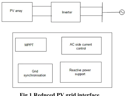
[image:1.595.329.546.460.625.2]The synchronization and current control play a significant role to meet the standards for the interconnection of PV to a utility grid [6]. The main disadvantage of the solar PV system they occupy large space to install a PV module. To extract the highest power from the PV source is the major problem in unsuitable conditions. Thus the optimal control can be taken out from the PV array with the help of micro inverter. The high-frequency transformers are used to increase the voltage or interconnect the PV array to the grid system. To reduce the large space for installing the transformer, the transformer is removed, and the micro inverter is used to reduce the drawback in the existing system. The cost-effective inverter solar PV is developed because of the growth in the semiconductor devices, controllers, and fall the rate in PV modules. In the PV module, due to the presence of parasitic capacitance and grounded metallic frame, they produce grounded leakage current. The leakage current, which increases the loss in the system, creates safety issues and unprotected to coordinate the operation. The main role of the transformer-less grid-connected inverter is to reduce the ground leakage current and to prevent the grid from the direct current.
Fig.1 Reduced PV grid interface
Figure 1 shows the reduced single stage PV-grid interface circuit. It consists of PV plants, MPPT controller, AC side current controller, grid synchronization, and reactive power support. Photovoltaic (PV) module converts the solar energy into the DC power. The dc power can be stored in the energy storage devices or directly connected to the inverter circuit. The filter circuit is used to inject a generated AC power to the grid and utilized by the loads. The reactive power support is used to inject voltage or current into the grid. The ac side current control is used to
control the grid current in the power system network. Thus, the electrical energy from the
Design and Implementation of Transformer less
Micro Inverter for PV-Grid Interface
PV module stored in the fuel cells.
II. INTERFACEOFPOWERCONVERTERSWITH PVSYSTEM
Photovoltaic (PV) array is mainly used to convert solar energy to electrical energy (i.e. Direct Current). The generated dc power is not directly fed to the grid because it is an ac system. With the help of power electronic converters or inverter this system is connected to the grid. According to the desired value of output voltage the inverters are connected in series or shunt combination. It can be operated in wide power range and hence it is easily transfers the generated PV power to the grid. The main aim of the transformer less micro inverter has to comply with
1. THD
2. Control voltage and frequency 3. Inject harmonic current 4. Grounding of the system 5. Synchronization 6. Islanding operation 7. Power factor
The requirement of grid-tied system is to extract the maximum power from the PV source and feed the generating power directly to the utility system without any storage devices. Fig.2. shows the block diagram of transformer less grid connected PV system. The main components of grid-connected PV system are as follows:
PV array
Inverter (DC-AC)
Filter circuit
Control devices
Cables
Fig.2 Transformer less grid connected PV system The main role of grid-connected PV system is to convert DC power to AC power. The PV array produce direct current (DC) power only but we need to AC power in the grid. The inverters do this task with high performance. The integration of PV and grid is a tedious task in the power system network. The inverter is used to integrate grid and PV system and delivers the good quality of power to the utility side.
III. OPERATIONANDFUNCTIONSOFPROPOSED
NOVELMICROINVERTER
A. Operation and function of micro inverter
Fig.3 shows the proposed transformer less micro inverter, which takes from the concept of Cuk converter. The neutral leakage current is eliminating with the help of connecting the grid neutral terminal to the PV module inverting terminal [8]. Table.1 shows the various modes of operation and switching connection. The input inductor (L1) is used for smoothing
operation. The peak overshoot occurs when the PV module interferes with the grid. The inductor (L1) is used to reduce the peak overshoot and also to improve the system performance and eliminate the delay time in the switches. The gate pulse will trigger easily and reduces the ripple current with the help of capacitor C1.
Fig.3 Proposed transformer less micro inverter Modes of operation described that first two modes are operates on non-inverting side and next two modes are operates on inverting mode side.
i. Mode I (S1, S3, and S4 ON)
A detailed operation of Mode I is shown in Fig.4. In mode I switches S1, S3, and S4 are ON. Switch S1 is ON condition, L1 gets store the charge from energy sources (PV).
ii.Mode II
Mode II operation classified into two sub-modes is described in Fig.5 (a) and Fig.5 (b). In Fig.5 (a) switch, S1 is OFF; the inductor L1 released their stored charge to C1 through diodes D2 and D3 respectively. The discharge way of capacitor C1 is sendto inductor L2, S4 and S3 to the grid. In Fig.5 (b) L2 discharge its energy through grid and S6.
Fig.4 Mode 1 operation
International Journal of Innovative Technology and Exploring Engineering (IJITEE) ISSN: 2278-3075, Volume-8 Issue-9, July 2019
Fig.5 (b): Mode 2 operation S3, S6 ON (iL1=0)
iii. Mode III
Fig.6. Shows the Mode III operation that S1, S2 and S5 are ON in condition. In Mode III and Mode IV, the switch S1 is operating on inverting side of the grid. The discharge path of the capacitor C1is bypassed through S2, S1, grid, and S5.
Fig.6: Mode 3 operation
iv.Mode IV
Mode IV operation classified into two sub-modes shown in Fig.7 (a) and Fig.7 (b).In Fig.6 (a) (iL1>0), the stored energy transfers from L1 to C1 takes place through D2 and D3. In Fig.7 (b) S1, S2 and S5 are ON in condition, (iL1=0) L2 sends the stored charge to S5 and D3 to the grid.
Fig.7 (a): Mode 2 operation S1, S2 and S5 ON (iL1>0)
Fig.7 (b): Mode 2 operation S1, S2 and S5 ON (iL1=0) Table.1: Modes of operation and inverter switching
connection
To prove the concept of the proposed system are taken by the following assumptions. The grid voltage (Vg) is constant over the switching period (Ts). The maximum power is injected to the grid by taking the inverter is lossless (assumed). In this case, the maximum power will be stored in the input inductor (L1).
whereVgmax and igmax is the voltage and current of the grid, L1 is the input inductor,
I2L1peak is the peak power stored in theinductor, Tsis the switching period.
B. Capacitor Voltage
At the time of high-frequency switching, the average current in the intermediate capacitor must be zero. The intermediate capacitor voltage Vc1 expressed as
C. Modulation Index
The discontinuous mode of operation of L1 leads to injecting high-quality power to the grid and ensures secure condition.
D. Input Inductor (L1)
The maximum power injects into the grid and ripple current are the two major sources to select the input inductor L1. TheequationforL1 is given below.
equated to the change in charge storage of C1 during OFF time (tOFF) of switch S1 as follows:
F. Secondary side Inductor (L2)
The secondary side inductor L2can be expressed as
G. Peak Voltage and Current
Except for S5 and S6 switches, the maximum current or voltage occurs in all the switches.
H. Primary side Capacitor (Cin)
The primary side capacitor Cin is used to reduce the peak input voltage is expressed as
I. Voltage Ratio
To balance the volt-sec of the inductors L1 and L2, the ratio of the maximum secondary voltage Voutpeak to the primary voltage Vin can be expressed as
IV. SIMULATIONRESULTS
(a)
(b)
(c)
(d)
Fig.8: Hardware Result (a) Input Voltage (b) Capacitor Voltage (c) Current across grid (d) Voltage across grid Hardware Description:
Reduced rated hardware is developed to validate proposed micro inverter. The 50W load is connected in the output side with the grid. IRF560 MOSFET is used as the switch. TLP250 MOSFET driver is used to switch to the MOSFET. Atmega 328 microcontroller is used to develop the switching pulses. Each switching voltage is isolated by separate isolation transformers. The hardware results are shown in above Fig.8: (a) Primary Voltage (b) Capacitor Voltage (c) Current across grid (d) Voltage across grid. The source voltage is transferred to capacitor C1 through inductor L1. When the switch S1 is operated, the source current is stored into capacitor C1. 12V solar panel is used to generate the input power of the microcontroller. The energy storage in the capacitor is shown in Fig.7 (a). The capacitor voltage is equal to 24V. During inverting and non-inverting side of the grid, the capacitor voltage is transferred to the grid through inductor L1 and L2 and voltage match transformer. The value of L1 is 320mH, L2, and L3 are equal to 740mH. The net voltage across the grid side is same as 230V. Harvested solar power is transferred through proposed micro inverter L1, L2, and C2are used to amplify the voltage of the micro inverter
V. CONCLUSION
The proposed method removes the ground leakage current and preventing injection of dc voltage into the grid is proposed for transformer less GCPVS. The different modes of operation are used to compensate both current-based and voltage-based power quality
issues.
International Journal of Innovative Technology and Exploring Engineering (IJITEE) ISSN: 2278-3075, Volume-8 Issue-9, July 2019
current from the PV array and gets the low output current distortion, reactive power support, and eliminate harmonics presents in the system. Reduced rated hardware was developed to validate the circuit, and the results are satisfying. Atmega 328 controller is used to get the desired output voltage.
REFERENCES
1. HcomonDehbonei, ChemNayar. “A Combined Voltage Controlled and current controlled ‘Dual converter for a Weak Grid-Connected Photovoltaic system with Battery Energy Storage.” IEEE Conference 011 Power Electronics Specialists.Vol. 3. Pp: 1495-1500.2002. 2. J.S. Siva Prasad and B.G. Femandes. “Active Commutated Thyristors
CSI for Grid-Connected Photo-voltaic Applications.” The 4m ICPEM, Vol. 3, pp: 1767-1771.2004.
3. AnastasiosCh et al. “Design and control of current source fly-back inverter for decentralized grid-connected photovoltaic systems.” European Conference on Power Electronics and Applications. Pp: 1-p.10, 2005.
4. G.Joos and, D. McGill et al. “The potential of distributed generation to provide ancillary services.” IEEE Power Engineering Society Summer Meeting., vol.3, pp. 1762-1767, 16-20 July 2000.
5. SorerenBaekhoejKjaer et al. “Power electronics as efficient interface in dispersed power generation system” IEEE Transactions on Power Electronics. Vol: 19, no.5, pp: 1184-1194, Sept 2004.
6. W.Lietel. “Topology review and derivation methodology of single-phase transformer-less photovoltaic inverters for leakage current suppression.” IEEE Trans. Ind. Electron., vol.62, no.7, pp.4537-4551, Jul. 2015.
AUTHORSPROFILE
A. Balamurugan is completed Master of engineering in applied electronics, Anna University, Chennai. B.E in Electrical and Electronics Engineering, Madras University, Chennai. Diploma in electronics and communication engineering in Director of technical education, Chennai and currently working as Assistant Professor in V.M.K.V engineering college, Salem.