International Journal of Innovative Technology and Exploring Engineering (IJITEE) ISSN: 2278-3075,Volume-8 Issue-6, April 2019
Abstract: The aim of this work is to propose a novel architecture for implementing Multiply Accumulate (MAC) unit which can be used to build a power efficient Digital Signal Processor (DSP). The proposed method uses hybrid parallel prefix adder in the multiplier stage and in the adder stage. The method improves the power consumption as well as the power-delay product. In the proposed architecture, a Han Carlson adder with modified pre-processing and post-processing stages (HCA_MPPS) is used in the Vedic multiplier and in the adder stage. The units are designed using Verilog Hardware Description Language (HDL) and simulated and synthesized for Artix-7 series Field Programmable Gate Array (FPGA) using Xilinx Vivado Design Suite 2015.2. The analysis showed that the proposed design has significant improvement in the power consumption and the figure of merit (power-delay product). The MAC unit employing modified Han Carlson adder has given a power saving of 11.38% and showed an improvement of 6.36% in the power-delay product.
Index Terms: Digital signal processor, Han Carlson adder, Modified Inequality detector, Multiply accumulate unit, Vivado design suite.
I. INTRODUCTION
Nowadays real time digital signal processing (DSP) finds a unique space in electronics industry due to its wide range of powerful applications. It involves tedious and rigorous multiplication as well as addition operations, which increase the computational and hardware complexity of modern digital signal processors. The performance of such digital signal processors largely rely on the efficiency of the multiplier units and adder units which are embedded within the processors. A typical multiplier block comprises of a series of AND gates to generate the partial products and an adder block to sum up the terms. The power consumption of these units has always been a crucial design concern for engineers. Many researchers have been working over the years to optimize the performance of multiplier and adder topologies.
The multiply-accumulate (MAC) unit is the main digital block used commonly and exhaustively in digital signal processors. It is an inevitable component in many digital signal processing applications which involves multiplications
Revised Manuscript Received on April 07, 2019.
Rakesh S, Department of Electronics and Communication Engineering,
Noorul Islam Centre for Higher Education, Thuckalay, Tamil Nadu, India and Mangalam College of Engineering, Ettumanoor, Kerala, India.
K. S. Vijula Grace, Department of Electronics and Communication
Engineering, Noorul Islam Centre for Higher Education, Thuckalay, Tamil Nadu, India.
and accumulations. For example, applications that require Fast Fourier Transform computations or Inverse Fast Fourier Transform computations, Finite Impulse Response filters, convolution, orthogonal frequency-division multiplexing algorithms can be efficiently implemented using MAC units. In this paper we propose a hybrid parallel prefix adder with modified pre-processing and post-processing (MPPS) stages. The basic MAC architecture consists of a multiplier, an adder and an accumulator register organized as in Figure 1. The inputs are given to the multiplier, and the result is added with the previous result stored in the accumulator register, leading to the accumulation process. Multipliers are typically a combination of a partial-product generation unit and a carry propagate adder to add the partial products to find the final sum.
Fig. 1: General architecture of MAC unit The rest of the paper is organized as follows. In Section II, the literature review has been explained in detail. Section III describes the methodology used in the proposed system. The simulation results are discussed in Section IV and finally the concluding remarks are given in Section V.
Modified Han Carlson Adder Based Multiply
Accumulate Unit for Low Power Digital Signal
Processor
II. LITERATUREREVIEW
There has been extensive research going on in the area of low power digital signal processing during the past two decades. Mohamed Asan Basiri et al. introduced a different floating point MAC structure compared to the conventional one. He combined the multiplier and adder block and formed a new block called multiplier-accumulator block and used Wallace tree for multiply accumulation process [1]. Tung Thanh Hoang et al. proposed a two’s complement MAC architecture which used a carry save adder as the final adder. The carry save adder contained 3:2 counters and it used shorter interconnects [2]. S Ahish et al. developed a MAC unit with a partial product reduction block and the multiplier was implemented using Brent Kung adder. The design achieved better area, delay and power performance compared to the conventional multiplier employing Booth algorithm [3]. Nithish Kumar V et al. incorporated a modified carry select adder at the multiplier stage of the MAC unit to improve the area. A digital filter is then designed using the MAC unit which achieved significant reduction in area and power [4]. Maroju Saikumar et al. introduced four different MAC architectures which employed carry save adder at the adder stage and four different multipliers. The four different multipliers used in the design were Array Multiplier, Ripple Carry Multiplier with row bypass technique, Wallace Tree Multiplier and Dadda Multiplier [5]. Narendra C.P et al. developed a partial product reduction stage using 29 compressors. Compressor architectures were also utilized in the carry propagation adder stage and accumulation stage [6]. A. Abdelgawad designed a merged architecture which combined the accumulation stage with the multiplier circuit. The speed and throughput of the MAC unit were increased and the area was decreased [7]. Suryasnata Tripathy et al. introduced a power efficient Vedic multiplier and realized using 45nm CMOS technology. He presented new design for 4-bit and 8-bit multipliers based on the URDHVA TIRYAKBHYAM (UT) sutra in Vedic Mathematics. The design was based on transmission gate logic and pass transistor logic. The design was realized using Cadence EDA tool with a 1V power supply by using several test inputs. The design showed improvement in speed, power consumed and chip area. The partial product generation unit designed using 5T AND gates helped to reduce the chip area. The UT sutra based design was responsible for the speed and power performance [8]. S.Rakesh et al. reviewed the design of different MAC unit architectures [9].
III. PROPOSEDMETHOD
In the proposed system a modified Han Carlson adder (HCA) is used for adding the partial products in the vedic multiplier and also at the adder stage. HCA belongs to the category of hybrid parallel prefix adder. The modification in this adder is done at the pre-processing and the post-processing stages. The pre-processing and post-processing stages consist of an inequality detector which performs exclusive OR operation. The inequality detector is designed here using four transistor logic. Switch level modeling is used to design the logic. The logic used is similar to the Gate Diffusion Input (GDI) logic [10].
Hybrid Parallel Prefix adder is a combination of
Kogge Stone adder (KSA) and Brent Kung adder (BKA). It takes the best feature out of both these adders ie high speed of KSA and low area of BKA. HCA uses Brent Kung stage in the first and last levels of carry computation and Kogge Stone stages in all the middle levels. So the speed is more for HCA due to the large number of Kogge Stone stages used in the carry computation [11].
Hybrid Parallel Prefix adders consist of a Propagate bit and Generate bit block (BGP) in the pre-processing stage, Group Generate and Propagate block (GGP) and Group Generate (GG) block in the carry computation stage and finally an inequality detector in the post processing stage for sum calculation.
BGP block generates the propagate bit
(1)
where Pi is ith Propagate bit, Ai is ith A input, Bi is ith B input,
xor is ‘xor’ operation in digital.
and generate bit
(2)
where Gi is ith Generate bit, Ai is ith A input, Bi is ith B input,
and is ‘and’ operation in digital.
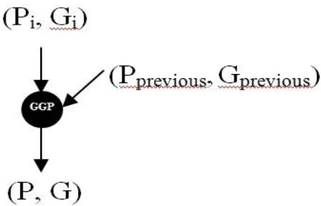
Figure 2 shows that GGP block generates
(3)
(4)
where G is Group Generate bit, P is Group Propagate bit, Gprevious is Generate bit from previous stage, Pprevious is
[image:2.595.326.554.508.654.2]Propagate bit from previous stage, + is ‘or’ operation in digital, . is ‘and’ operation in digital.
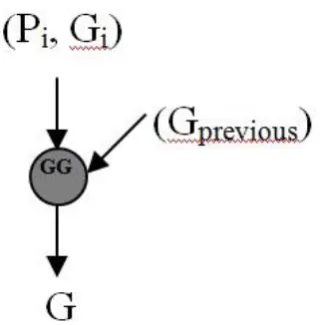
Fig. 2: Generation of Group Generate and Propagate bits Figure 3 explains that GG block generates
International Journal of Innovative Technology and Exploring Engineering (IJITEE) ISSN: 2278-3075,Volume-8 Issue-6, April 2019
[image:3.595.98.259.51.214.2]Fig. 3: Generation of Group Generate bit Figure 4 clearly shows how the GGP block and GG blocks are used to compute the carry at different stages of HCA. The expressions for the generation of carry C0 to C7 are also given
[image:3.595.57.289.299.457.2]in (6) to (19).
Fig. 4: Structure of a 16 bit Han Carlson Adder (6)
C1 = G1 + P1 C0 (7)
(8)
(9)
(10)
(11)
(12)
(13)
(14)
(15)
(16)
(17)
(18)
(19)
The carry bits are used to compute the final sum using the
expression given in (20).
(20)
Thus the pre-processing stage uses an inequality detector to compute the “Propagate bit,Pi” from the input bits Ai and
Bi. The post processing block also uses an inequality detector
to generate the final “sum bit, Si”. Inequality detector
[image:3.595.305.547.434.573.2]performs exclusive OR operation. It gives a high output when the inputs are unequal and hence the name inequality detector. The modified inequality detector is designed using the switch level modeling in Verilog HDL code. It is implemented using 4 MOS transistors out of which there are 2 PMOS transistors and 2 NMOS transistors. The conventional transistor implementation of the inequality detector needs 12 MOS transistors out of which 6 are NMOS transistors and 6 are PMOS transistors. Figure 5 shows the circuit diagram of the modified inequality detector. Thus there is a reduction in the number of transistors in the circuit which reduces the power consumption appreciably and improves the figure of merit (power - delay product) also.
This will pull down the output to ground potential. Low swing can be caused at the output when A=0 and B=0. In that case we expect the output to be zero but due to the poor high to low transition characteristics of the pmos, the output will be VTp. [12-14]. The proposed architecture of the multiply
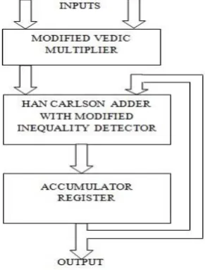
[image:4.595.304.550.51.135.2]accumulate unit that can be used in a Digital Signal Processor is given in Figure 6. The architectures employ a modified Vedic multiplier which uses a modified hybrid parallel prefix adder to sum up the partial products. At the adder stage also the modified hybrid parallel prefix adder is incorporated to add the result of multiplication and the previous result stored in the accumulator register. The accumulation process is actually taking place at the adder stage. The final result is again stored in the register. The accumulator register is basically a parallel in parallel out shift register.
Fig. 6: Proposed MAC Architecture
IV. RESULTSANDDISCUSSION
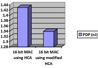
The simulation results of the modified inequality detector and the proposed MAC unit architecture are presented in Figure 7 and 8 respectively. Also the power reports generated are shown in Figure 9 and 10. A comparison between the existing MAC design and the proposed design is given in Table 1. The comparison table clearly reveals that the proposed 16 bit MAC design using modified Han Carlson adder has given a power saving of 11.38% and showed an improvement of 6.36% in the power-delay product. A graphical comparison of the power and power-delay product of the two MAC architectures is presented in Figure 11 and Figure 12 respectively.
[image:4.595.302.553.59.753.2]Fig. 7: Simulation result of modified inequality detector
[image:4.595.302.549.185.440.2]Fig. 8: Simulation result of 16 bit MAC unit with modified Han Carlson adder
[image:4.595.103.249.254.446.2]Fig. 9: Power report of 16 bit MAC unit with Han Carlson adder
Fig. 10: Power report of 16 bit MAC unit with modified Han Carlson adder
Table 1: Comparison of MAC Architectures
Architectures On Chip Power
(W)
Power Delay Product (nJ)
16 bit MAC using Han Carlson
Adder 0.123 1.430
Proposed 16 bit MAC using Modified Han Carlson Adder (HCA_MPPS)
0.109 1.339
0.1 0.105 0.11 0.115 0.12 0.125
16 bit MAC using HCA
16 bit MAC using modified
HCA
Power (W)
[image:4.595.301.554.441.712.2] [image:4.595.44.297.655.752.2]International Journal of Innovative Technology and Exploring Engineering (IJITEE) ISSN: 2278-3075,Volume-8 Issue-6, April 2019
1.28 1.3 1.32 1.34 1.36 1.38 1.4 1.42 1.44
16 bit MAC using HCA
16 bit MAC using modified
HCA
[image:5.595.86.284.60.197.2]PDP (nJ)
Fig. 12: PDP comparison of 16 bit MAC architectures
V. CONCLUSION
The proposed design of MAC unit using modified Han Carlson Adder which employs a modified 4 transistor inequality detector in the pre-processing and post-processing stages is found to be an efficient design in terms of power consumption and power-delay product or figure of merit. It is evident from the performance analysis that the design showed an improvement of 11.38% in the power consumption and 6.36% in the figure of merit. So the power efficient design may be widely used for several data intensive digital signal processing applications such as fourier transform computations, filter design etc. In future focus may be given in reducing the delay further thereby trying to improve the speed of the system.
REFERENCES
1. M. Mohamed Asan Basiri and Sk. Noor Mahammad, “Configurable Folded IIR Filter Design”, IEEE Transactions on Circuits and Systems -
II: Express Briefs, Vol. 62, No. 12, pp. 1144 – 1148, 2015. 2. Tung Thanh Hoang, Magnus Själander and Per Larsson-Edefors, “A
High-Speed, Energy-Efficient Two-Cycle Multiply-Accumulate (MAC) Architecture and Its Application to a Double-Throughput MAC Unit”, IEEE Transactions on Circuits and Systems - I : Regular Papers, Vol. 57, No. 12, pp. 3073 – 3081, 2010.
3. S. Ahish, Y.B.N. Kumar, Dheeraj Sharma and M.H. Vasantha, “Design of High Performance Multiply-Accumulate Computation Unit”, Proceedings of IEEE International Advance Computing Conference (IACC), pp. 915-918, 2015.
4. V. Nithish Kumar, Koteswara Rao Nalluri and G. Lakshminarayanan, “Design of Area and Power Efficient Digital FIR Filter Using Modified MAC Unit”, Proceedings of IEEE International Conference on Electronics and Communication Systems, pp. 884-887, 2015.
5. Maroju SaiKumar, D. Ashok Kumar and Dr. P. Samundiswary, “Design and Performance Analysis of Multiply-Accumulate (MAC) Unit”, Proceedings of IEEE International Conference on Circuit, Power and Computing Technologies (ICCPCT), pp. 1084-1089, 2014.
6. C.P. Narendra and Dr. K.M. Ravi Kumar, “Low Power MAC Architecture for DSP Applications”, Proceedings of IEEE International Conference on Circuits, Communication, Control and Computing (I4C), pp. 404 – 407, 2014.
7. A. Abdelgawad, “Low Power Multiply Accumulate Unit (MAC) for Future Wireless Sensor Networks”, Proceedings of IEEE Sensors Applications Symposium (SAS), pp.129-132, 2013.
8. Suryasnata Tripathy, L.B. Omprakash, K. Sushanta Mandal and B.S. Patro, “Low Power Multiplier Architectures Using Vedic Mathematics in 45nm Technology for High Speed Computing”, Proceedings of IEEE International Conference on Communication, Information & Computing Technology (ICCICT), 2015.
9. S. Rakesh and K.S. Vijula Grace, “A Survey on the Design and Performance of various MAC Unit Architectures”, Proceedings of IEEE International Conference on Circuits and Systems (ICCS), pp. 312 – 315, 2017.
10.A. Askhedkar and G. Agrawal, “Low Power, Low Area Digital Modulators using Gate Diffusion Input Technique”. Journal of King Saud University –
Engineering Sciences, 2017,
http://dx.doi.org/10.1016/j.jksues.2017.08.001.
11. R. Tackdon Han and David A. Carlson, “Fast Area - Efficient VLSI Adders”, Proceedings of IEEE 8th Symposium on Computer Arithmetic
(ARITH), pp. 49 – 56, 1987.
12. Waleed Al-Assadi , Anura P. Jayasumana and Yashwant K. Malaiya, “Pass-transistor logic design”, International Journal of Electronics, Vol. 70, No. 4, pp. 739-749, 1991.
13. A. Morgenshtein, A. Fish, I. A. Wagner, “Gate-Diffusion Input (GDI): A Power Efficient Method for Digital Combinatorial Circuits”, IEEE Transactions on VLSI Systems, Vol. 10, No. 5, pp. 566-581, 2002. 14. I. S. Abu-Khater, A. Bellaouar and M.I. Elmastry, “Circuit Techniques for
CMOS Low-Power High-Performance Multipliers”, IEEE Journal of Solid-state Circuits, Vol. 31, No. 10, pp. 1535-1546, 1996.
AUTHORSPROFILE
Rakesh S received B.Tech. degree in Electronics and Communication Engineering from Mahatma Gandhi University, Kottayam, Kerala, India in 2008. He obtained Masters in Engineering in VLSI Design from Anna University, Chennai, Tamil Nadu, India in 2013. He is currently a research scholar in Noorul Islam Centre for Higher Education, Thuckalay, Tamil Nadu, India. His research interests include Digital VLSI design, Low power VLSI design etc.
Dr. K. S. Vijula Grace received her B.E degree in