Rochester Institute of Technology
RIT Scholar Works
Theses
Thesis/Dissertation Collections
11-1-2000
Development and characterization of a sub-micron
CMOS process as an educational tool at RIT
Ivan Puchades
Follow this and additional works at:
http://scholarworks.rit.edu/theses
This Thesis is brought to you for free and open access by the Thesis/Dissertation Collections at RIT Scholar Works. It has been accepted for inclusion in Theses by an authorized administrator of RIT Scholar Works. For more information, please [email protected].
Recommended Citation
DEVELOPMENT AND CHARACTERIZATION OF A SUB-MICRON
CMOS PROCESS AS AN EDUCATIONAL TOOL AT RIT
by
Ivan Puchades
A thesis Submitted
in
Partial Fulfillment
of the
Requirements for the Degree of
MASTER OF SCIENCE
in
Electrical Engineering
Approved by:
PROF: --'-A..;.;,.lb;.:..e~r....:..t.;;....;H.;..."T;..;.it~u....:..s _
(Thesis Advisor)
PROF: _
PROF: _
PROF: _
(Department Head)
DEPARTMENT OF ELECTRICAL ENGINEERING
COLLEGE OF ENGINEERING
ROCHESTER INSTITUTE OF TECHNOLOGY
ROCHESTER, NEW YORK
THESIS RELEASE PERMISSION FORM
COLLEGE OF ENGINEERING
ROCHESTER INSTITUTE OF TECHNOLOGY
Title of Thesis:
DEVELOPMENT AND CHARACTERIZATION OF A SUB-MICRON CMOS
PROCESS AS AN EDUCATIONAL TOOL AT RIT
I, Ivan Puchades, hereby grant permission to the Wallace Memorial Library of the
Rochester Institute of Technology to reproduce the thesis in whole or in part. Any
reproduction will not be for commercial use or profit.
Signature
!~/
0/
LCOOTable
ofContents
LIST OFTABLES v
LIST OFFIGURES vi
1. INTRODUCTION 1
2. BACKGROUNDANDLITERATUREREVIEW 6
2.1. ICManufacturingEducationatRochester InstituteofTechnology 6
2.2. ProcessBackground 14
2.2.1. Advanced CMOS processTechnology 15
2.2.1.1. Historical TrendandPredictions 15
2.2. 1.2. ScalingRequirements 17
2.2.1.3. IdealScalingvs. ActualScaling 18
2.2. 1.4. First ScalingChallenges- Submicron Devices 21
2.2.1.4.1. Substratedoping 21
2.2. 1.4.2. LightlyDoped Drains
-High energycarriers and short-channel
effects 25
2.2.1.4.3. Shallow
junctions-Xj 32
2.2.1.4.4. Gateoxideintegrity
-tox 34
2.2. 1.5. Latest Developments 37
2.2.2. RlT's CMOS P-wellProcess 45
2.2.2.1. Substrate Preparation 46
2.2.2.3. Interconnects 50
2.2.2.4. Test 51
2.2.2.5. SPICE Parameters 59
2.2.3. RIT's Submicron CMOS Process 65
2.2.3.1. SubmicronCMOS Design 66
2.2.3.2. Submicron CMOS Process 69
2.2.3.2. 1. Substrate Preparation 70
2.2.3.2.2. Build Transistors 72
2.2.3.2.3. Interconnects 74
2.2.3.2.4. Test 75
2.2.3.2.5. Device Simulation 79
3. PROCESS IMPROVEMENTS 85
3.1. Lithography- 1
urnResolution 87
3.2. Etch 88
3.2.1. Polysilicon Etch 88
3.2.2. LTO Etch- SpacersandContactCuts 90
3.3. Diffusion 93
3.3.1. PadOxide 93
3.3.2. Well LOCOS Oxidation 94
3.3.3. Twin-Well Drive 95
3.3.4. Field Oxide Growth 96
3.3.5. Sacrificial Kooi Oxide 96
3.3.6. Gate Oxide 97
m-3.3.7. Poly DopingDrive-in 98
3.3.8. Spacer Densification 98
3.3.9. D/S ActivationAnneal 99
4. PROCESS DETAILS 102
5. TESTRESULTS , 138
5.1. ProcessTesting s 139
5.1.1. NMOS 139
5.1.2. PMOS 140
5.2. NMOS SPICE Parameters 146
5.3. Recommended Test Improvements 150
6. CONCLUSION AND FUTURE WORK 152
APPENDIX 154
A. PROCESS PICTURES 155
B. Silvaco's SUPREM SIMULATION INPUT FILES 173
List
ofTables
Table 2.1a. PredictedprocessdevelopmentsatRTT 13
Table 2.1b. HistoricalTrend-Moore'sLaw 15
Table 2.2. 1994and 1996 SAIRoadmap 16
Table 2.3.IdealScalingRules 18
Table2.3. Comparisonof advanced processes 44
Tabel2.4.Teststructures and parameters extractedintheRITP-Well CMOS Process..52
Table2.5. SummaryofrecentRIT P-Well CMOS Test Results [5] 68
Table 2.6. Summaryof simulation resultsfor 0.5umdevices 79
List
ofFigures
Figure 2.1. Short-channeleffects 17
Figure 2.2. Microtec Simulation- Typical
Retrogradewelldoingprofile 24
Figure 2.3. Lateralcomponentofthesurface electricfield 26
Figure2.4.IGvs. VGwithVDof10V, 12V and 14V [20] 28
Figure2.5.Fabricationsequence ofLightlyDopedDrains 29
Figure2.6.Verticalelectricfield for LDDvs. Non-LDDtransistors 30
Figure 2.7Surfacepotentialinthechannelforlongand shortchanneldevices. Linear
and saturatedVtroll-off effects 31
Figure2.8. Typicalthreshold-voltage roll-off as afunctionof gatepoly-Silength fora
setdrainvoltage 32
Figure 2.9. Oxide breakdownfrequency as afunctionof appliedfield 34
Figure 2.10. Inversion layer junctions [31] 43
Figure2.11. Processcross-sectionafter substratepreparation 48
Figure 2.12.Processcross-section. Completedtransistors 50
Figure2.13. Processcross-section. Completed inverter device 51
Figure 2.14.Test-chiplayoutfortheRIT P-Well CMOS Process 53
Figure 2.15. Van Der Pauwstructureusedin Sheet Resistanceextraction 54
Figure 2.16. CrossBridge Kelvinteststructure forcontact resistance 55
Figure 2.18. NMOSFET layoutstructure 56
Figure 2.19. P-WellandN-welldopingprofiles afterdrive-in 71
Figure 2.20. Processcross-section after substrate preparation 71
Figure 2.21. LDD's junctionprofiles 74
Figure2.22. Processcross-section. Completedtransistors 74
Figure 2.23. Processcross-section. Completedinverter device 75
Figure 2.24. The Submicron CMOS ProcessTest-Chip Layout 77
Figure 2.25. Differentsize capacitorsto studygate oxidequalityVTshifts 78
Figure 2.26. DifferentsizeNMOS transistorstostudy VTroll-offand short channel
effects 78
Figure3.1.Micrographsofthinnedgatelines 88
Figure3.2. Anisotropy 89
Figure3.3.Over-etched Contact Cuts 90
Figure3.4. Fabricationsequence ofLightlyDoped Drains 91
Figure 3.5. Contact Cut Etch SEM 92
Figure 3.6. Twin-well Cross-section. SUPREM Simulation output 95
Figure 3.7. Twin-well junction depths 96
Figure 3.8.FOXandKooiOxideSUPREM Simulation 97
Figure 3.9.N+ andNLDD SUPREM Junction Depth Profile 99
Figure 3.10. P+andPLDD SUPREM Junction Depth Profile 100
Figure 4.1. 1st
LevelLithography- N-well. SUPREM Simulation
106
Figure 4.2.After N-well Oxidation. SUPREM Simulation 109
Figure4.3.After Twin-Well Drive. SUPREMSimulation Ill
Figure 4.4. Alignmentandresolutionverniers 113
Figure 4.5. After Channel StopImplant. SUPREM Simulation 115
Figure 4.6. AfterField Oxidegrowth. SUPREMSimulation 117
Figure 4.7.VtpAdjust Implant. SUPREMSimulation 120
Figure 4.8.AfterPolyetch. SUPREM Simulation 125
Figure 4.9. AfterSpaceEtch Back. SUPREMSimulation 129
Figure4.10. After D/S Anneal.SUPREM Simulation 133
Figure 5.1. Micrographshowingthe l.lum polygate 140
Figure 5.2a,b. Thresholdvoltage extrapolation and familyof curvesfor NMOS 140
Figure5.3. Familyof curves of aPMOS transistor 141
Figure5.4. Low resistance pathbetweensource anddrain areasofthePMOS
transistors 142
Figure 5.5. Drain todrainresistance 143
Figure5.6. Lowresistance pathbetweenthedrainareas oftwodifferent PMOS
transistorsinsidethen-well 143
Figure 5.7. Lowresistance pathbetweenthedrainareas oftwo different PMOS
transistorsin differentn-wells 144
Figure5.8. A leakagepath existsinthep-well 145
Figure5.9. Terada-Muta Method for extracting Leff 148
Chapter 1
Introduction
1. Introduction
Rochester Institute of Technology is recognized worldwide for its educational
programs and laboratory facilities in the area of microelectronic manufacturing
engineering. In this state-of-the-art facility, graduate and undergraduate students design
and manufactureintegratedcircuitsusingPMOS, BJTandCMOS technologies.
In a recent article published in the December 1999 edition of Solid State
Technology magazine, author Stanley Wolf expresses his concern about the lack of
cohesive education programs for IC manufacturing in the U.S. He also concludes that
there is "a shortage ofengineering graduates, especially those from the pioneering and
renowned IC manufacturing program atthe Rochester Institute of Technology (RIT).
Numbering about 35-55/year (approximately 30 BS, 10 MS, and 3 PhDs), the RIT
graduates are only a small fraction of the engineers entering IC manufacturing every
year."[l]
InordertokeepprovidinghighlyqualifiedengineersRITmustkeeppace withthe
rapid evolution ofthe IC manufacturing industry, thus RIT must continuously improve
exclusively using Submicron CMOS process technology. This implies that RIT must
improve its CMOS processto theSubmicronregionalso.
AnadvancedSubmicronCMOSprocesshasbeen developed and characterizedfor
use at RIT. The new process features many advance device structures such as dual well,
sidewall spacers andlow-doped drains.
This project starts withthe literature review ofthemostrecent as well as the not
so-recent advances inthe front end ofIC manufacturing. The frontend is defined as the
manufacturing steps that deal with the fabrication of the transistorper se, prior to a
secondlevel of metaldeposition. It doesnotincludeprocesses such as CMP oranyother
planarization techniques. Although enormous improvements have been developed in the
areas, these are not included inthis work due to the vastcomplexity this would entail. It
also goes beyondtheprocessdeveloped inthis thesisand reviewsthelatest developments
upto thefutureyear2010andbeyond.
It also reviews what is currently the most advanced process at the RIT Factory
lab, the CMOS P-Well Process. It presents the sequential process steps and aid tools
which are availabletoall students.A summary ofthe most recent results anddevice data
isalso presentedinthissection.
Thebasis forthe developmentofthisprojectistheworkof graduate studentSuraj
Bashkaranin the developmentofthe RIT's Sub-Micron CMOSProcess. His work looks
at the design consideration as well as the process flow andboth process simulation and
RIT has developed a large base of previously successful technologies. The new
process is an evolution from these previously successful technologies. The majority of
the project is developed on existing equipment, using modified versions of proven
process sequences. Theseprocess improvements arepresentedin Chapter 3. Atypical IC
manufacturing process is divided in production groups. Each ofthese groups develops
theirown processes tolaterintegratethem togetherwiththeothers. Asimilarapproachis
followed in this project. Separate process steps are developed independently and then
integratedtogether when needed. When avalid process alreadyexists, this is used as is.
The separate processing disciplines and the improvements generated in each are
described below. The integrationof alltheseimprovements ispresentedin Chapter 4.
Processing pictures, which are included in the appendix of this thesis, are also
available at every step of the process as a visual aid in determining the proper action
when problems arise. Thesetwo aids are akeyplayerto the successful completionofthe
process.
Two 3-wafer lots where exclusivelyprocessedat RIT usingthe newly developed
Submicron CMOS Process flow, which is described in detailed in chapter 4. The
electrical test ofthese two lots show promising results although some work must still be
done to further improve the device characteristics. The NMOS and PMOS devices are
tested for functionality and SPICE parameters are extracted when possible. Some
assumptions are made when extracted SPICE parameters and these are noted. The
assumption of some key values is necessary in order to overcome some non-idealities
brought about by a design error. Due to a design error the PMOS devices do not show
3-transistorcharacteristics and theNMOS deviceshave anextremely large leakage current
at OV gate bias. The root cause of this error has been investigated and a solution has
alreadybeenputintoplace.
Due to the successful completion of this project, students from the
Microelectronic department of RIT will use this process flow starting in the winter
quarter of2000. They will follow thenewly developedprocessinthefabrication oftheir
designed IC's. Theextraction ofSpiceparameters will also allow the accurate simulation
of these designs prior to their fabrication. This will place RIT at the top of the
Universities offering semiconductor-manufacturing programs and will help further
References
1.
Chapter 2
Background
and
Literature
Review
2.1 ICManufacturing EducationatRochester InstituteofTechnology
Stanley Wolf is the well-renowned author of the three-part series Silicon
Processingforthe VLSI Era and owner ofLattice Press. In a recent articlepublished in
the December 1999 edition of Solid State Technology magazine, Wolf expresses his
concern about thelack ofcohesive education programs for IC manufacturing in the U.S.
Wolf points out that despite the imminent need of IC manufacturing Engineers on the
work place, and although "engineers and scientist are well educated in specific
disciplines, such as electrical engineering, chemistry, physics, materials science,
mechanical engineering, and optics, they still enter the industry untrained for IC
manufacturing. By-and-large, even at theengineeringlevel, trainingin IC manufacturing
is stilloccurring onthejob" [1]. AccordingtoWolf, engineering educationhas failed to
change and supportwhatisthecornerstoneindustryintoday's society,ICmanufacturing.
Wolfs perspective comes from seeing the shortage ofrecent, up-to-date semiconductor
textbooks. Fourofthefivetop-sellingtextbooksonthesubjecthavecopyrightdatescirca
1990. This means that the most modern developments in technology, which have
Finally, he concludes with a statement that has been the motivation for the
developmentofthis thesis work;
"There is a shortage ofengineering graduates, especially those from the pioneering and renowned IC manufacturing program at the Rochester
Institute of Technology (RIT). Numbering about 35-55/year
(approximately 30 BS, 10 MS, and3 PhDs), the RIT graduates.are only a smallfractionoftheengineers enteringIC manufacturing every
year."
Other universities which have IC Manufacturing facilities include, Boise State
University, University of Illinois, Standford, MIT, UC Berkely, UCLA, University of
Michigan, University of Texas Austin, Arizona State University, National Chiao Tung
University and others [6]. The laboratory courses offered by these universities follow
along the lines ofthe more traditional hands-on courses taught at RIT. Although much
researchisconductedintheseuniversities,this is mainlyundertakenby graduate students
and in only very specific subjects. The uniqueness of the Rochester Institute of
Technology laboratory is its capability of completing a CMOS process by its
undergraduate students andfabricatingcomplex circuit anddevices.
Rochester Institute of Technology started its Microelectronic Engineering
program in 1986. Graduates from this program are highly sought after by leading
Semiconductor companies and are often commended on their preparation and
performance as they reach the work place. The success ofthis programis greatly due to
the excellent clean room facility, which is available to all students, undergraduates and
graduates alike. RIT has invested heavily inthehands-onteaching methodology. The IC
laboratory at RIT is one ofthe largest at any universitywith a cleanroomfloor space of
over 15,000 square feet [3]. The facility has a complete equipment set for the
7-manufacture of silicon integrated circuits on 4 inch and 6 inch diameter wafers. The
equipment includes, IC Design Tools, Electron Beam Maskmaking, 1 GCA g-line
stepper, a Canon Mine stepper, ASM 248nm Excimer Laser Stepper, 193nm Excimer
laser Lithography System, Low Pressure Chemical Vapor Deposition system, Varian
120-10 Ion Implanter, Varian 400-10 Ion Implanter, Wafer Coat and Develop Systems,
Reactive Ion Etch systems, Wet Etch and RCA Clean Benches, Surface Analysis
Systems, Spectroscopic and Ellipsometric Metrology Tools, Profilometer, Chemical
Mechanical Polishing, Electrical Test and Probe Systems and Scanning Electron
Microscopy.
Several courses take advantage of these facilities with classic laboratory
participation such as Microlithography I and U and Thin Films. At these middle-level
courses, students are passive participants on a traditional laboratory experience. The
instructor, with the help of a graduate assistant, performs well-rehearsed experiments
during which the students learn basic IC manufacturing techniques. All these courses
complementthreehour/weeklectures, whichpresentanddiscussthe topicscoveredin lab
aswellas others.
Students also become familiarized with a variety ofIC manufacturing processes
such asthecompletefabricationoffourmask-levelMetalGate PMOS transistorsontheir
sophomore yearaswellas a triple-diffusedNPN BJTprocess [2] duringtheirfourthyear.
As in atraditional university IC laboratory, students take a few wafers and start at step
These classes, for the most part, follow the concurrent (hands-on) teaching
methodology describedbyAzavedo[4]. Thisteachingmethodologyfacesthe"paradoxes"
and pitfalls presented by the more classical method ofteaching: sequential teaching. In
sequential teaching the curriculum is organized by following the logical or historical
structure ofthesubjects tobestudied. Thecontent is divided intotopicsand eachtopicis
presented in depth. "The focus is then on programmatic content and clarity of
exposition". Theclass presentationsexpose fixed protocols forpredetermined problems
and solutions where "The teacherpossesses all theknowledge". Azavedo recognizes the
pitfalls ofthe sequential teaching methodology by saying that students are "reduced to
memorizing names and algorithms"
[4]. The above-mentioned courses address these
issues by creating open-ended experiments during laboratory. Students use previously
learnt skills such as designofexperiments ordevicephysics tocreatetheirown courseof
action to resolve a specific problem presented by the teacher. The teacher becomes a
mere consultanttothestudents project. Oncetheprojecthas beencompleted, the students
presentthe findings to the rest oftheclass and answer questions from the teacher. Their
gradeis basedontheexperimental designand amounteffortputinto solvingtheproblem
as well as on their final understanding ofthe issue. A faulty experimental process does
not mean a failing grade as long as the students can comprehend the issue under study
andexplaintheirmisconceptionsandhow thecorrectedthem.
On the study and evaluation of a similar course taught at San Jose State of
University [5], researchers found that students felt that they have learned more than in
traditionalclassrooms. Inthe study,25%ofthestudents indicatedthattheywereinactive
9-in the classroom. In contrast, all of them thought that they were active or moderate
participants inthelaboratory.
During theirfifth andlastyear, undergraduate students at RIT take an even more
untraditional type of course, an IC Manufacturing Laboratory using a student operated
factory[3]. Inthis course aP-Well CMOS processis used asan educational tool toteach
advanced manufacturing processes. The students in the course are the operators for the
factory. The instructor is the shift manager and the different laboratory sections are the
different shifts. Typically inone schoolterm there are4 to 6 shifts in aweek. Eachshift
begins with a shift meeting where the shift manager reviews the status ofthe lots in the
factory. Assignments are made for each operator based on lot selection rules and
equipment availability and the past experience of the operator. In this factory the
operators are encouraged to do operations that theyhave notdone before and to average
twolot moves per shift. Depending onthenumber ofstudents in the lab section and the
queue status operator assignments are made. At the beginning of the school term
operators are usually assigned in pairs to work on lots. Towards the end ofthe school
term assignments are made one lot per student. The instructor and teaching assistant
rotate around lab from operator to operator helping with some details, answering
questions, asking questions and solving problems. The students keep a lab notebook to
documentwhattheydideachweek,includingobservations,dataand other entries.
The fact that students act as operators could raise some concerns on the actual
learning accomplished. This is acommon problemwith mostlaboratoryexperiences and
moving lots into their pertinent processing steps, students must be able to identify at
whichstep thatparticularlot is and whether or notithas beenprocessedcorrectlytothat
point. Thentheymustcorrectlyperformthe steptheyhavebeenassigned and understand
how it ties to the 200-step process and how it would affect the final product. Finally, if
problems arise, the student mustbe able toidentify a course of action to remedy it. This
is all done with the aide ofthe instructor and several other resources such as in process
monitoringandmetrologytools.
This course could be classified as a extreme of concurrent teaching [4]. Again,
concurrent teaching exposes student to concrete engineering problems that require
knowledge ofthe contents of the discipline. It places them, as much as possible, in the
shoes of the engineer in that he student describes the problem, devises a solution and
presents and/or manages it. In this teaching methodology knowledge is constructed,
althoughbasic knowledge ofthe basic processes is required. The students work and the
teacher supervises guiding them inthe right direction. Students become problem-solvers
and are comfortabletakingupnewchallenges.
Thiscourse also overcomes the twoparadoxes ofengineeringeducationfoundby
Azavado,theparadoxofmultidisciplinaryandtheparadoxofthespecialist.The.paradox
of multidisciplinary deals with the need of combining multiple disciplines in solving a
problem. With theincrease interaction and integration oftechnologies, multidisciplinary
problems ariseconstantly.According toMuscatetal.,Microelectronic device fabrication
is inherently interdisciplinary [5]. Each of the basic processes draws upon a varied
spectrum of subjects such as physics, chemistry and chemical material, electrical
engineering. Although all these subjects have been studied by Microelectronic
Engineering students at RIT during the previous years, it is not until the presentcourse,
ICManufacturingLaboratory, thattheygettointeractalltheirknowledge. Thissimulates
whattheywillbedoingintheworkforce.
The second is theparadox ofthe specialist. Azavado considers it "impossible to
teach alltheknowledgethat an engineeris expectedtouse today".Teachersdo notknow
what will be required for engineers to know in the future. It is also impossible to teach
everything in the allotted amount of time. On the other hand, this course provides
students with the skills andunderstanding necessary to tackle any engineering problems
thatmayarise attheworkplacewithconfidence.
There is nodoubt that the Factory course has become avery useful learning tool
for students. Onthe other hand, the RIT P-Well CMOS process used in this course was
developed eight years ago. Unfortunately, as the IC manufacturing industry has been
developing,it has fallen alongthelines described abovebyWolf. It does notinclude any
ofthemost moderndevelopments in technology,whichhave happened in thelate 1990's.
The manufacturing development of a Sub-Micron CMOS process is proposed.
This would take advantage of the most advance equipment available in the RIT
Microelectronic Manufacturing facility. This equipment is capable of Sub-Micron
resolution,whichwouldbeusablefor Logic designas wellasAnalogcircuitry.
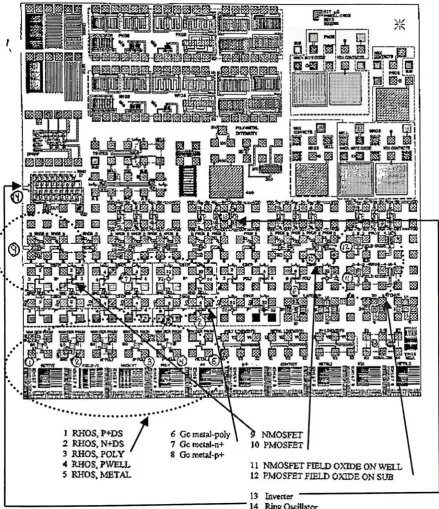
Table 2.1a summarizes the advances that are included in the RIT's Submicron
positon RIT in a level where advance research that would benefit the microelectronic
industrycanbeconducted.
The completion of this project would benefit the RTT College of Engineering
enormously. Not only would undergraduate students be exposed to the most advanced
manufacturing processes but graduate students from the Electrical Engineering,
ComputerEngineering andMicroelectronicEngineeringdepartmentswould alsohavethe
chancetoactuallyfabricatingtheirownICdesigns inatimelymanner.
Present Process Submicron RIT Process
,\,^,..>,^.,.-v,;.'..-,.,i.S,
Advanced RIT Process
P-Well
PMOS+NMOSVtadjustI
j
MinimumCD: 4-micron GCA G-line Stepper LOCOS Isolation 500A GateoxideN+-polyGate
Analog/Digital 12V/5V Design lambda= 3-micron
"RIT's design
rules"
100mmsubstrate
Twin-Well No VTadjustI
MinimumCD: 1-micron
CanonI-line LOCOS Isolation 150A Gateoxide
Gatespacers andLDDs
N+-polyGate '-
-Analog/Digital 5V/5V Designlambda=0.5-micron
MOSIS designrules
150mmsubstrate
-Twin-Well No VT-adjust I
Minimum CD: 0.5-micron ASML Excimer Laser STI Isolation
100A Gateoxide
SpacersandLDDs TiN Contact/Metal Liner Dualdoped poly Gate Analog/Digital
Designlambda=0.25-micron
MOSIS designrules
150mmsubstrate
[image:23.504.63.487.271.544.2]2000 2001
Table 2.1a. PredictedprocessdevelopmentsatRIT
2.2Process Background
The following sections deal with the most recent as well as the not so-recent
advances in the front end of IC manufacturing. The front end is defined as the
manufacturing steps that deal with the fabrication of the transistor per se, prior to a
secondlevel of metaldeposition. Itdoes notincludeprocesses such as CMP oranyother
planarization techniques. Althoughenormous improvements have been developed inthe
areas, theseare notincludedinthisworkduetothevastcomplexitythiswould entail.
The first section deals with the main advances developed in the 1990's and that
are not included in the current RIT CMOS P-Well Process. It also goes beyond the
process developed inthis thesisand reviews thelatest developments upto the future year
2010andbeyond. Thesecond section explains whatis currently done at the RIT Factory
lab, the CMOS P-Well Process. It presents the sequential process steps and aid tools
which are availableto all students. A summaryofthemostrecent results anddevice data
is also presented on this section. The third section reviews thework of graduate student
Suraj Bashkaran inthedevelopmentofthe RIT'sSub-Micron CMOS Process. It looks at
the design consideration as well as the process flow and both process simulation and
2.2.1 AdvancedCMOS process
Technology
MOSFET miniaturization has been anissue ofstudyever since the development
of the first integrated circuit. According to [7], large-scale-integrated circuits (LSI's)
appeared in the early 1970's with the introduction of a 1-kb dynamic random access
memory DRAMand a 0.75-MHzmicroprocessor
using 10-8um PMOS technologies [7].
Digital and memory circuit applications benefit the most from the scaling down of
MOSFET devices. Smaller dimensions mean higher packing density and either more
memorystoragecapabilityorfaster switchingspeedfor logictechnology[8].
2.2.1.1 HistoricalTrendandPredictions
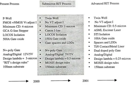
According to Moore's law [9] the number oftransistors per chip would double
every 18 months orincreaseby afactor offour everythree years. This prediction, made
in 1975, has heldtrue for over 25 year. Table 2.1b shows how this trend has been very
closely followedhistorically[7].
Year 1974 1977 1980 1983 1986 1989 1992 1995 1998
Sizeum 6.0 4.0 3.0 2.0 1.2 0.8 0.5 0.35 0.25
Shrinkrate 0.67 0.75 0.67 0.6 0.67 0.63 0.70 0.71
DRAM 4K 16K 64K 256K 1M 4M 16M 64M 256M
Table 2.1b. Historical Trend- Moore's Law
The Semiconductor Industry Association (SIA) published in 1994 a roadmap for
semiconductors topredicttheevolutionoftheindustryuntil theyear2010 [10]. Thiswas
15-later revised in 1996 and although it shows a slight slow down in the shrinking rate, it
still follows Moore's law accurately [11]. Table 2.2 presents these two trends predicted
bySIA.
Year 1995 1998 2001 2004 2007 2010
Sizeum 0.35 0.25 0.18 0.13 0.10 0.07
Shrinkrate 0.71 0.72 0.72 0.77 0.70
DRAM 64M 256M 1G 4G 16G 64G
YEAR 1997 1999 2001 2003 2006 2009 1012
Denselines:Halfpitch(um) 0.25 0.18 0.15 0.13 0.10 0.07 0.05
Shrinkrate 0.72 0.83 0.86 0.77 0.7 0.71
Isolated Lines: gate(um) 0.20 0.14 0.12 0.10 0.07 0.05 0.035
Shrinkrate 0.70 0.86 0.83 0.70 0.71 0.70
DRAM @ introduction 256M 1G 4G 16G 64G 256G
DRAM @ production 64M 256M 1G 4G 16G 64G
Table2.2. 1994and1996 SAIRoadmap
This trend is likely to be followed since there have been announcements of the
fabrication of0.15 um, 0.1um and evensub-O.lum MOSFETdevices by several authors
at the research level [12] [15]. These authors have reported on the good operation of
these devicesat roomtemperature andthetechniquesutilized fortheir fabrication. These
[image:26.504.37.485.177.479.2]2.2.1.2ScalingRequirements
In digital circuit applications, a MOSFET functions as a switch. Ideally, in the
"off state no current shouldflow and low resistance orhigh currentshould bepresentin
the"on" state. Smallcapacitancesare alsoimportanttoallow rapidswitching.As thegate
lengthdecreases, itbecomes difficulttosimultaneouslymeetthesetworequirements.
In small devices, even in the "off state, due to the proximity of the drain and
source ofthe device, theleakagecurrent fromsource to drainincreases. This is the
well-known short channel effect of the MOSFET's [7]. The extension of the drain
space-charge region is suchthat it touches the sourceregion as soon as avery small voltage is
appliedto the gate, thuscreating alower-than-designedthreshold voltage, alsoknown as
drain induced barrier lowering (DIBL) effect, and lager leakage characteristics in the
"offstate (Figure 2.1). Thesuppressionof short-channel effects is oneofthe mainareas
ofinterestwhenshrinkingthedevicedimensions.
OV
OV Vdd
Gate
Source Drain
"\, Space Charge Region
Figure 2.1. Short-channeleffects
Smallergatelengths are desirableinthe
"on"
statebecause itreduces thechannel
resistance oftheMOSFET 's. When this channel resistanceequals thatofthe source and
drain regions, the device cannot be improved. Thus, reduction ofthe source and drain
resistances is necessary inordertomakescalingeffective.
To summarize, thescalingofMOSFET devices is onlyeffective ifimprovements
oftheMOSFET performance areaccomplished. These improvementsare often related to
newfabrication andmanufacturingtechniques.
2.2.1.3 IdealScalingvs.ActualScaling
In order to suppress short-channel effects and secure good switching
characteristics, Dennard et al. [16] proposed an idealized scaling method. Using this
method, theparameters oftheMOSFET deviceare shrunk orincreasedby afactor ofK.
Table 2.3 shows how each parameter is modified by K. Thus, the space charge layer
would be reduced with the reduction in channel length, leading to the suppression of
short-channel effects.
Scaling rule(Ideal) Gate lenqth(Lg) 1/K
Parameter Scale Gatewidth(Wq) 1/K
Gate Area(Sg) 1/K*2
CD > o w "to c (0 1 H
Gate lenqth(Lq) 1/K Gateoxide(tox) 1/K
Gatewidth (Wq) 1/K Supplyvoltaqe 1/K
Gateoxide(tox) 1/K Q)
_)
Gatecapacitance(c)~Sq/tox 1/K
Junction depth(xj) 1/K Gatecharge(Qg) ~Cg*V 1.KA2
Sub, imp.Cone. (Nsub) K Propaqationdelay (tpd) ~Qq/ld 1/K
Drain Voltaqe(Vd) 1/K Clockfrequency (f) ~1/tpd K
DrainCurrent(Id) 1/K NumberofTransistors(n) K*2
Thresholdvoltaqe(Vth) 1/K Chipsize(Sc) ~n*Sq 1
Propaqationdelay(tpd) 1/K Power(P)-0.5
* f*
n*C*
V*2 1
This method also calls for a reduction of the power supply by a factor of 1/K,
which in turn would result in a current reduction by the same factor. The increase on
number oftransistors is also determined atK2. The powerconsumption andchiparea are
also keptconstant. Had this ideal scaling been followed since 1974, the most advanced
LSIsystems wouldbe 1-Mb DRAMand34MHzmicroprocessors [7].
Fortunately for the microelectronic industry, the ideal scaling method was not
followed. The supplyvoltage was not changedintheearlystages ofMOSFET scaling[7].
This was done in orderto keep a compatibility with the supply voltage ofconventional
systems and alsoto obtain ahigher operating speed underhighelectric fields. The supply
voltage was not reduced untiltheelectric field across thegate oxide reached the electron
tunneling limit of ~4MV/cm. This occurred during the development of the 0.5um gate
length MOSFET technology; whenthe gate oxidethickness approached 120A.
In 1980,Brewset al. [17] derived an empiricalrelationship betweentheminimum
length and other device parameters; this must be kept in order to obtain long channel
behavior. Theproposedempirical relationforanNMOStransistoris:
L^^OAl-lxjtJw.+wj]", (2.1)
where L^ isthe minimum channel length forwhichlong-channel behavioris observed,
A is a proportionality factor, xi is the junction depth, tBX the oxide thickness and
ws+wdthe sum of source and drain depletion depths in a one dimensional abrupt
junctionformulation. Suchthat:
19-"< =
JzQPWk
+vbi+VBS)j'2
andtheDebyelength,
(2.2)
r -11/2
LB =
faNA
(2.3)with
fi=
kT
-1-1
(2.4)
VDSis drain-to-sourcevoltage, Vbiis thebuilt-involtageofthejunctions and VBS=0. NA
is theimportantfactorof substrate concentration orNsub foraNMOSFETdevice.
This empirical relation provides an estimate for MOSFET size reduction without
the needfor shrinking all dimensionsbythe same scalefactor. This flexibilityallows the
choice of otherthanstrictlyscaledgeometries,"new geometries which are easierto make or which optimize other aspects ofMOSFEToperation"
[17].
The minimum channel length necessary in order to avoid short channel effects
and its dependence to the physical dimensions ofthe drain junction depth
x-, the oxide
thickness tox, andthedepletion layerwidth ws +wd,was also observedby Zhi-HongLiu
et al. [18]. In this work, a threshold voltage model for MOSFET 's is derived using a quasi-two-dimensional approach. This model is based on the solutions ofthe
quasi-two-dimensional Poisson's equation in the depletion region. In their case the characteristic
lengthvalue is definedas,
withXj, Xdepand inum andTox inA.
They conclude that a simple scaling rule is that the channel lengthmust be at least five
times the characteristic length . Thus, =-^-, which agrees with the empirical
prediction madein 1980, andemphasizestheneedforcontrol ofthe threekeyparameters
drain junctiondepthXj, theoxidethickness tox,andthedepletion layerwidth Xdep.
2.2.1.4 FirstScalingChallenges- Submicron Devices
The active regiondeterminesthearea where thedevices arebuilt. This is thearea
wherethetransistorper se is built. The scalingconsiderations forthe activeregionofthe
transistors must include the three important factors mentioned above, drain junction
depthXj, theoxidethickness tox,andthe depletion layerwidth
Xdep
.2.2.1.4.1Substratedoping
The depletion layer width Xdep, calculated from the one dimensional
abrupt-junctionapproximationresultsinthe expression,
\2-Si-{2-<j>F)
XA, = r"*.
TF'
(2.6)
dep n q-N
SUB
which shows the inverse proportionality of the depletion width dimension with the
substrateconcentration.Accordingtoboth,theidealand empiricaltheoriesofscaling, the
value ofthe substratedoping concentrationmustbe increased inordertoreducethevalue
ofthedepletionregion.
Historicallythe substrate
doping
concentration of eitherthe PMOS ortheNMOSdevice was closely controlled by the formation of a n-well or a p-well in the starting
silicon substrate. The challenge ofCMOS technology is to fabricate side by side on the
same chip bothNMOS and PMOS transistors. Thus creating silicon regions of opposite
polarity to provide local substrates for the complementary transistors [20]. These wells,
besides beingoftherightpolarity, also provide electricalisolationfromeach other under
every operating condition. They are biased with the supply voltage, which ensures a
reversebias condition[21].
The first CMOS IC's employed the single-well technique, which was used for
several yearsdue toits simplicity [22]. Thistechnique formsan opposite polaritywell in
thestartingsubstrate, usuallyat thebeginning oftheCMOS process. This wellis formed
byionimplantation, followedbyalongdiffusion athightemperatureand aselective field
oxidation.
P-welltechnologywas developed first. Beforetheavailabilityofionimplantation,
surfaceinversionundertheNMOS fieldcould notbe easilyeliminatedin CMOS without
the use of area-consuming "guard rings". With the capability ofcontrolling the p-well
doping, the boron segregation into the field oxide and the effect of fixed oxide charge,
which would lead to charge inversion and a low NMOS field threshold, could be
compensated. Thus, a NMOS field transistor of higher threshold was created [21].
Another reason for the use of this technology was the better "gain matching"
between
concentration in the p-well, and the consequent carrier mobility reduction, could
compensateforthelower mobilityofholecarriers.
Theuse of an n-well wasdeveloped as soon asion implantationbecameavailable.
This approach took advantage of the already dominant NMOS technology since these
devices could still be fabricated in the silicon bulk with the only addition of PMOS
transistors in the n-well. NMOS devices are inherently faster due to the higher electron
mobility at comparable lithographic resolutions. An added advantage is the ease of the
transition toBiCMOS technologyduetothepresence of an n-well,which can serve as an
electrically isolatedcollector.Ann-well alsoimprovedlatch-up immunity [22].
The advantages of single well processes start to vanish as minimum feature size
decreases [21]. It becomes moredifficultto optimizeboth NMOS andPMOS transistors.
To match the characteristics of a NMOS transistor to those of a PMOS using a p-well
process,a well surface concentrationmustbeaboutfivetimeshigherthan thatofthebulk
substrate. Thus, this requires a low doped starting substrate, which is susceptible to
punch-throughbetween thedepletion layers ofthe scaleddownsource and drainregions.
Thesolution forthis is a deepphosphorous punch-through prevention implant, followed
by a shallow boron threshold adjust implant. Also, the well lateral diffusion and the
extension ofthedepletion layer in the lightly dopedside, the siliconbulk side,constrain
the minimum spacing between NMOS and PMOS devices, not allowing for an increase
ondevice density.
The alternative twin-well presents an integral solution to these problems. Each
well is formed separately by doping it at a higher concentration than the substrate. The
23-wells aresymmetricallyformedandtheNMOS andPMOS devices formedand optimized
independently. On theotherhand,twin well technologydoes notincrease devicedensity.
Even though the well border is located close to its drawn position, as opposed to the
single well process where design rules or an extra mask step where necessary to
compensateforlateral welldiffusion, welldiffusion is still aproblem. Alongwell
drive-in isstillnecessarytodiffusethedoping,thuslateral diffusion is stillpresent.
Adding to this problem is the requirements for high substrate concentrations.
Accordingto [8],for 1 urndevicesadopingconcentration of
lE16/cm3
is sufficientbut it
results intoo low of athreshold voltage. Asurface threshold adjustimplantis enough to
achieve the required threshold. On the other hand, as the channel doping concentration
approaches values of lE18/cm3 to prevent drain to source punch-through, the resultant
threshold voltage becomes too high [8], close to the supply voltage. In this case, a
retrograde dopingprofile is needed (see figure 2.2). The thresholdvoltage is lowered to
thedesiredvaluewhile stillmaintainingpunch-throughcontrol.
0. 0.3 0.6 0.9
DistanceY(microns)
Figure 2.2. Microtec Simulation - Typical Retrograde
welldoingprofile.E=500KeV, Arsenic,
Retrogradewells areformedby
high-energy
ion implantationoncetheactive areaisolation structures are already in place, thus
preventing the problem of impurity
segregation. Afterthe retrogradeimplant, thermal steps arekept to a minimumin order
toretaintheoriginalimplantprofile. Rapid ThermalAnnealreactors (RTA)have become
veryusefulfor this. This prevents impuritydiffusion towards the surface ofthe channel,
which wouldinterferewiththedesignedthreshold voltage[21].
Another major benefit of retrograde wells is a significant increase in device
packing density compared to twin well technology. Well lateral diffusion is practically
eliminated since nohightemperature step is necessary after implantation. Thisallowsfor
more closely packed CMOS devices. The retrograde well technique is beingused in the
most advanceddevicesand seems tobethe trendforthecoming years.
2.2.1.4.2LightlyDoped Drains
-High energycarriers and short-channel effects
As channel length dimensions get smaller, there is a reliability issue concerning
channel hot carriers due to the high longitudinal electric fields. Lightly doped drain
(LDD) FET structures wereintroducedto deal withthis issue [25]. This structure creates
a series resistance withinthesource anddrainterminals whichhelplowerthevalue ofthe
electric fieldinthe channel, thusreducingtheenergyofthechannel carriers.Incidentally,
it was later shown that the LDD structures could also reduce another kind of short
channel effects: thresholdvoltage roll-off[22].
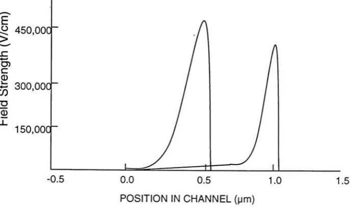
25-At the saturation value of
VDS
, highelectric fields are found at the drain end ofthe channel. Figure 2.3 shows thechannel lateral electric field values forboth long and
short channeldevicescalculatedinsimulation[21].
-0.5 0.0 0.5 1.0 1.5
POSITION IN CHANNEL(um)
Figure2.3. Lateralcomponent ofthesurface electricfieldas afunctionof channellength.
The extremely large values ofthe electric field nearthe drain junction cause hot
carrierinduced degradation in bothp- and n-channelsMOSFET duetoimpact ionization
of electron-hole pairs [19]. An electron, with energy in excess of the conduction band
minimumby more than the semiconductor bandgap, can transfer its energyto a valence
electron, thus creating an additional conduction electron and valence hole. A positive
feedbackcondition iscreatedin which more impact ionizationsoccur. The resultanthigh
currentis detrimental and caneasily damagecircuit components andit mayeven leadto
[image:36.504.99.444.162.365.2]Another problem with high-energy carries occurs as these encounter a
semiconductor-dielectric interface. Thin gate oxides separate the gate from the channel.
These gate oxides have been getting thinner as channel dimensions have been shrinking
in orderto maintain adequate gate control over the channel. Ideally there should be no
flow of channel carriers intothegate dielectric since apotential barrierof3.2eVprevents
these from reaching the oxide. But, as mentioned previously, the high electric fields
encountered near the drain end of a MOSFET create a certain amount carriers with
enough energy to surmount the silicon-silicon dioxide barrier and tojump into the gate
[26]. The number of carriers with enough energy to reach the gate terminal can be
measured by monitoring the gate current. Figure 2.4 shows such a measurement. For
fixed drain bias, the gate current peaks at a particular gate bias. The decline in gate
current beyond the maximum is due to the decreasing channel electric field with the
increasinggate bias.
~<0
J*'
,a-i _
10.
ia-J
in-10""
io-"
V-1AV
Ve-12V
Vo=iOV
&
is-i<s ssi
[image:38.504.120.414.71.371.2]24-Vo. i'V5
Figure 2.4. IGvs.VGwithVDof10V, 12Vand 14V[26].
Carrier emission into the gate oxide will also lead to charge trapping within the
oxide. Although typical silicon dioxide films only trap about one percent of the total
number ofinjectedelectrons this results ina charge accumulation within the gate oxide,
which will affectMOSFET behavior [27]. The thresholdvoltage change ofthesedevices
isminimalduetothehighlylocalizedtrappingnearthedrainterminal[21].
It isalsoimportanttonotethatalltheparameters thatare scaledduringMOSFET
miniaturization, (i.e. drain junction depthx-}, theoxidethickness tox,and substratedoping
The lightly doped drain (LDD) FET structure was introduced to lower the drain
electric field [25]. Figure 2.5 shows the fabrication sequence ofthese structures. A light
implant is donemaskedby thegate. The implantation doseofthis LDD implant is about
two orders of magnitude less than that of the source-drain region. A conformal
depositionof silicondioxideisdoneright afterthision implantation. Ahighlyanisotropic
dryetch ofthe silicon dioxide will leave a spaceralong the sidewalls ofthegate.A final
high-energyimplant isperformed andthedrainandsourceareas areformed.
/ uate ux
Poly /
/ \ *
/
\
FOX 1
[
FOX]
N
^
n-V
\ /
l-)
FOX
Poly
n-
n-FOX
FOX
N+ n- n- N+
[image:39.504.145.389.266.656.2], FOX
Figure 2.5.FabricationsequenceofLightlyDoped Drains.
The LDD region provides a transition area between the channel and the
highly-doped source and drain. Thus, theelectric field maximum is reduced since the potential
presents a more gradual transition. Figure 2.6 shows the lateral electric field component
inthechannel with and withouttheLDD structure [36].
?
2. UJ cc
!->
a
_j
id
LUUUUU
.NoLDD
ChUMNEHLMSYH; 1jw.
pxirjr.thichmesb:W>m i
dSftOOO ACCEPTOR CONIC: EEi-S KACC
;:
300JOCC
!
J|
k WithLDDf<?0
/
y
, \^
-o.s O.o at i,o
[image:40.504.84.451.181.405.2]POS-ITIONINC^ANNei. farn]
Figure 2.6. Verticalelectricfield for LDDvs.Non-LDDtransistors.
l.S
Added advantages of LDD structures include the capability of generating self
alignedlow-resistancesilicidedcontacts, which willbeexplained later,andthe reduction
oftheVtroll-off effect.
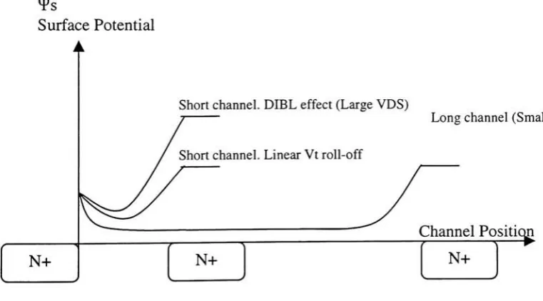
Thereduction in threshold voltage withdecreasingchannel lengthand increasing
drain to source voltage is used as an indication of short-channel effects [18]. As
mentioned previously, due to the proximity ofthe drain to the source terminal, the gate
potential necessary to turn the device "on"
cause a reduction inthepotential energy barrier thatopposes the entry of electrons from
then+ sourceintothechannel, inthecase of anNMOS device. Thisreduction(knownas
theDrain Induced Barrier Lowering or DIBL) makesthe turn-on easier [24]. These two
effects are known as linearVt and saturated Vt roll-off (DIBL) respectively. Figure 2.7
shows the two Vt roll-off mechanisms that affect a NMOS. The surface potential along
the channel is plotted for different channel lengths. While the turn-on surface potential
has been determined to 2<pF. As the channel length decreases the minimum surface
potential along the channel increases near the 2<pF value. Also as VDS is increased on
same sizetransistors,theminimumsurface potentialinthechannelalsoincreases.
s
Surface Potential
N+
Shortchannel.DIBLeffect(LargeVDS)
Shortchannel.Linear Vtroll-off
Longchannel(SmallVDS)
ChannelPositi
N+
)Sition
[image:41.504.60.441.324.535.2]N+
Figure 2.7 Surfacepotentialinthechannelforlongandshort channeldevices.
LinearandsaturatedVtroll-off effects.
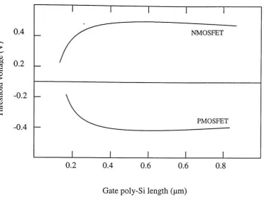
Typical Vt roll-off measurements used to characterize short channel effects of
CMOS transistors is shown in figure 2.8, this is done by plotting the effective channel
length ofNMOS transistors and their thresholdvoltage [18]. A comparison ofLDD vs.
non-LDD devices with equal channel lengths has shown that LDD structures are
beneficialand reducetheVTroll-off effect [18].
0.4
>
g 0.2
4
"o
>
o
1)
H
-0.2
--0.4
-1 1 1 1 1
_
/^
NMOSFET
\^^
PMOSFET1 1 1 1 1
0.2 0.4 0.6 0.6 0.8
[image:42.504.60.433.113.395.2]Gatepoly-Silength(um)
Figure 2.8. Typicalthreshold-voltage roll-off as afunctionof gate poly-Silength fora setdrainvoltage.
2.2.1.4.3 Shallow junctions
-xy
In orderto maintain long channel characteristics while scaling down the size of
MOSFET devices, a very shallow junction of the drain terminal is necessary. The
junction depth ofthis device depends on manyfactors, such as ion implant energy and
subsequentthermal treatments.
Arsenic is currently being used to create the n+/p junction on NMOSFETs.
Arsenic doesnot favor channeling because it is aheavyatomand as such ittends notto
>0.1u\m. In another technique, in order to obtain abrupt ultra-shallow junctions, a
pre-amorphization ofthe silicon surface with species of opposite polarity has been used by
some researchers [12]. Ultra-shallow junctions have been obtained with
pre-amorphization by indium, followed with a low-energy arsenic implant. 50nm junctions
were created onthefabricationofthisadvanced nFETby [12].
The problem arises in the formation of the p+/n junctions of the PMOSFETs.
Boron hastraditionallybeenused asthe sole impurity dopingtoformp-typeregions. B+,
being a small and light atom would require very small implant energies to create the
necessary shallowjunctions, (i.e. 5-10KeV). This can be alleviated with the use of the
BF^ion. Higher energyimplants canbe used since theB+ion only acquires 22% ofthe
BF1^ energy [28]. However, the main concern is the channeling of
B+
ion through the
Siliconcrystal. BF+2astheimplanted speciesis also affectedbythiseffect sinceit breaks
on impact [29]. Other techniques such as implantation through a thin Si02 layer,
crystallographic miss-orientationorthesurfacedamagecausebythe fluorine ionsare not
efficientin suppressing the B+channeling [30]. This has been accomplished onlyby the
pre-amorphization oflarge atoms such as Si+, Ge+
[30]. Shahidi andhisteamobtained a
junction depth of 60nm by preamorphizing the substrate with Sb+[12]. A low energy
BF2+
wasthenperformedtoobtainanabrupt shallowjunctionat adepthof60nm [12].
Once this shallow-junction structures are createdbymeans ofionimplantation, it
is important not to disturb this distribution during the activation anneal. Rapid thermal
annealing has emerges as the solution to thisconcern. Using high-intensityarc lamps or
lasersources, thismethod isableto separatethe activationanddiffusionoftheimplanted
ions [28].
2.2.1.4.4 Gateoxideintegrity -tox
Thinner gate oxides are a requirement in scaling CMOS devices. A thinner gate
oxide will allows a faster and more efficient transistor action as well as reduced
short-channel effects.
However, gate oxide wear-outis one ofthemostmenacing failure mechanisms of
MOS devices. The silicon dioxide insulator may break and create a conductive path
betweenthe gate and the substrate,rendering theCMOS device useless. It is known that
higher electric fields acrossthe insulating gate oxide lead to early oxide breakdown and
device failures. Figure 2.9 shows this oxide breakdown frequency distribution as the
electric fieldacross theoxideis increased.
U z w D
w
O
<
100
80
60
40
20
0
BMODE
CMODE
A MODE
1
0 5
BREAKDOWNFIELD(MV/cm)
The earlier and almost immediate failures arise from gross defects within the
oxidefilm. These failures are
usually easilydetected,and thedevicesthathavethem, are
eliminatedfromthemanufacturingproduct line. Another groupof oxide samples willfail
atfairlyhighelectricfields of>7MV/cm andmayfunctionproperly for many hours. This
high field failure mechanism is known as intrinsic failure. It is well understood and
devices are designedso as not tooperate inthis region. Thethird groupof oxide samples
is intermediateto theimmediatefailures andintrinsicpopulations.These devices abruptly
break at any fields between 2-6MV/cm after many hours of operation. This presents a
problem sinceCMOS miniaturizationhas resultedin mostdevices beingoperated in this
region. For example a typical 0.75|im process using a supply voltage of5V employs a
gate oxidethicknessof 15nm,i.e. 3.3MV/cm [31]. Anotherprocess utilizes a3.3V supply
with 12.5nmgate oxide,2.7MV/cm [32].
This breakdown mechanismis not fullyunderstood although subtledefects in the
oxideintegrity are presented as responsible forthisbehavior. This ispresumed since the
intrinsicpopulation assures usthatdefect-free silicondioxide shouldbeableto withstand
theseintermediateelectricfields.
Experimentally, current flow from the gate to the substrate material is observed
prior to intrinsic breakdown. This current flow through the insulator is associated to
Fowler-Nordheimtunneling. Bythismechanism, electronsinthesubstrate (anode)tunnel
through the energy barrier into the oxide and drift to the gate (cathode) [21]. This
tunnelingcurrentisoftheform,
I =AE exp2 f~B^
v* j
(7)
where E is the electric field and A and B are often termed constant. Thus, the oxide
current is exponentially dependenton the electric field. Experiments have shown that as
the electric field is increased, the gate current followsthisexponential relation shown in
equation 7 upto thepoint ofbreakdown.
The intrinsic breakdown mechanism points to a Fowler-Nordheim electron
tunneling injection into the oxide in ahighelectric field, which leads to hole generation
by impact ionization and net hole trapping within the oxide. Thus, net positive charge
accumulation dueto this high-field impactionization, increasesthe cathode field so that
electroninjection also increases. This positivefeedbackproduces alocal current density
thatdestroystheoxide structure [24].
Returning to the intermediate group of oxide breakdown, understanding this
breakdown mechanism is of outmost importance. As described previously, CMOS
miniaturization requires IC circuits to operate at field strengths of 2-7MV/cm. Sodium
contamination has been easily recognized a source of oxide breakdown. The positive
sodium ions tend to migrate towards the cathode, enhancing the local electric field and
thus increasing electron injection. This field enhancement continues until the oxide
breaks. It is alsobelieved thatoxidedefects may effectively lowerthebarrier for
Fowler-Nordheim tunnel injection of electrons into the oxide conduction band. The breakdown
mechanism is then identical to that of the intrinsic group, only shifted to lower fields
It is also important to note that thinner oxide should lead to reduced impact
ionization due simplyto the limited spatial extent ofthe oxide conductionband in which
the electrons possess enough energy to ionize a valance electron. This indeed favors
MOS technologyandminiaturizationand contrasts againsttheincreasingelectricfieldsat
which gate oxides are operating.
A method to avoid oxide damage over time is tooperate at lower electric fields.
Fowler-Nordheim injection has been determined to start at values of4.5MV/cm. CMOS
devices are designedandtheirparameters adjustedto operate at electricfields below this
limit. It has also been determined that to obtain a better quality oxide, slow growth and
high growth temperature are desirable [33]. Finally, "clean" processing with minimal
contamination,maximumgetteringandhigh-qualitystartingmaterials areallnecessary in
ordertoobtain goodquality,defect-freeoxide [21].
2.2.1.5 Latest Developments
The development from sub 0.25umto0.1|im gateCMOS has beenthe interestof
researchfor manygroups overthepastfew years. Severalnew manufacturingtechniques
have been developed in order to overcome the scaling difficulties. These include the
advances described above such as retrograde wells, LDD structures, shallow junctions
andthin gateoxides inadditiontodual doped polygates,salicidedcontacts,nitrided gate
oxides and several novel device isolation techniques. Most ofthepapers reviewed here
present devices fabricated in research laboratories. The mass production of these, with
someexceptions,isstill awaitingtheintroductionoflithographic advancementsAs such,
the method used to determine the gate length has been specified whenever applicable.
Finally, this section concludes with abriefreview of sub0.1urn devices, which predicts
the transistorsofthefutureupto the year2010.
Shahidi et al. [12] reports in the fabrication ofCMOS devices with a minimum
channel length below 0.1p.m to demonstrate the potential of this technology for the
manufacture of0.1 5um CMOS transistors. Highly nonuniform channeldoping and very
shallow drain/sourceextensions are usedinatwinwellprocess. The wells aredopedwith
Indium and antimony in order to obtain highly un-uniform dopingprofiles with implant
peaks are placed at about lOOnm under the channel via ahigh-energy implant of about
190KeV. The polysilicon gates are dual doped, which assures surface channel devices,
and patterned using e-beam lithography to obtain channel lengths bellows 0.1um. The
thin gate oxidethicknessis only 4.5nm [12].
Ultrashallow source-drainjunctions are obtainedby preamorphizationbyindium
and antimony followed by a low energy implant of As (NMOS) and BF2 (PMOS)
respectively. Counter-doping with the preamorphizing species results in a more abrupt
junction and better device characteristics. The NMOS junction is approximately 50nm
fromthe surface and the PMOS is approximately 60nm fromthe surface. Thick spacers
are used to place the deeper heavily doped source-drainjunctions far from the channel
and avoid short channel effects. A titanium silicide process is used over the drain and
source contactstominimize sourceanddrainsheetresistance[12].
The electrical results show gooddevice parameters and characteristics. Electrical
BarrierLowering which are usually affected by short channel effects, show acceptable
values. The subthreshold slope is 85mV/decade and 90mV/decade for the NMOS and
PMOS devices respectively for threshold voltages of 0.35V and -0.35V. Threshold
voltage roll-off is not observable above Leff of 0.07um and the drain-induced barrier
loweringis only 150mVand no punch-through isobserved [12].
Y. Mii et al. [14] worked on a high performance sub-0.lp.rn channel
NMOSFET's. Ultrathingate oxides (3.5nm), retrograde channel doping profile, shallow
source-drain junctions and low series resistances are the tools used to fabricate these
devices. A room temperature delay of 11.3ps/stage is reported, which is the fastest
switching speed reported to date of publication for any silicon devices at room
temperature. The cutofffrequency ofthese devices is 94GHz at 300K and 119GHz and
85K, which is accomplished with lowered capacitance values. Good subthreshold
characteristics are also reportedwith minimal short-channel effects [14].
In 1995, Yukio Okazaki et al. [34] reports on the fabrication of a dual poly-Si
gateCMOS processinvolvingseparate depositionsofin-situ doped
n+
and
p+
poly-Si for
the NMOS and PMOS transistors respectively. These transistors have effective channel
lengthsof0.2jxmand atthingateoxidesof3.5nm.Thispaper presentsaCMOSoscillator
cut-offfrequencyof5.78GHz [34].
Dual doped poly-Si, as mentioned previously, assures surface channel behavior
and better gate controllability. The gate material must be doped as
p+
type in order to
create surface channel PMOS devices. The mainconcern isboron diffusivitytrough the
polysilicon gate andpenetration intothe thin gate oxide. A nitrogen-dopedPoly-Si layer
is used here to prevent boron penetration. This layer is deposited by (low pressure
chemical vapor deposition) LPCVD prior to the deposition, also by LPCVD, of the
boron-doped poly-Si layer. This (multilayer boron
![Figure 2.4. IG vs. VG with VD of 10V, 12V and 14V [26].](https://thumb-us.123doks.com/thumbv2/123dok_us/121167.11681/38.504.120.414.71.371/figure-ig-vs-vg-vd-v-v-v.webp)