Internal Current Return Path for Ground
Leakage Current Mitigation in Current
Source Inverters
University of Nottingham Ningbo China, 199 Taikang East Road,
Ningbo, 31
5
100, China
First published 201
9
This work is made available under the terms of the Creative Commons
Attribution 4.0 International License:
http://creativecommons.org/licenses/by/4.0
The work is licenced to the University of Nottingham Ningbo
China under the Global University Publication Licence:
Date of publication xxxx 00, 0000, date of current version xxxx 00, 0000.
Digital Object Identifier 10.1109/ACCESS.2017.DOI
Internal Current Return Path for
Ground Leakage Current Mitigation in
Current Source Inverters
E. LORENZANI
1
, (Senior Member, IEEE), G. MIGLIAZZA1,2
,(Student Member, IEEE)F. IMMOVILLI1, (Senior Member, IEEE), C. GERADA2, (Senior Member, IEEE), H. ZHANG2, (Senior Member, IEEE), G. BUTICCHI2, (Senior Member, IEEE)
1
DISMI - Department of Science and Methods for Engineering, University of Modena and Reggio Emilia, Reggio Emilia, Italy
2
Zhejiang Key Laboratory on the More Electric Aircraft Technologies, University of Nottingham Ningbo China, 315100, Ningbo, China Corresponding author: G. Buticchi (e-mail: [email protected]).
This work was supported by the Ningbo Science & Technology Beauro under Grants 2018A-08-C, 2013A31012, 2014A35007.
ABSTRACT This paper analyzes in detail the effect of a simple solution for ground leakage
currentmitigation applicable to transformerless three-phase Current Source Inverter (CSI). The circuit modification solution is assessed for both traditional CSI topology and for CSI with an additional seventh switch, in literature named CSI7 (or H7), in particular with the splitting of the DC input inductance. In the present work the solution is applied to grid-connected converters for string photovoltaic applications: scope of the circuit modification is to provide an internal return path from the wye-connected capacitors of the output CL filter. This additional return path is able to significantly reduce the ground leakage current without adversely affecting THD. The performance of the proposed solution is assessed by numerical simulations in case of a string of PV modules and the different behavior of CSI and CSI7 topologies is thoroughly investigated. Furthermore, the
definition of VcmZC is assessed by applying it to the common mode equivalent circuits for CSI7 with additional return path and their validation by means of a two-step simulation. Simulation results and experimental validation show good agreement and confirm that the proposed solution is able to strongly reduce the ground leakage current.
INDEX TERMS current source inverter, photo-voltaic power systems, ground leakage current,
renewable energy sources.
I. INTRODUCTION
URRENT Source Inverter (CSI) topologies consti-C
tute an alternative solution to the Voltage Source In-verter (VSI) paradigm, and they have been exploited for medium voltage applications [1]. Because of the intrinsic voltage boosting behavior and with the development of high-frequency switching devices, they have been investigated for single-stage photovoltaic (PV) inverter solutions [2], [3]. Because no electrolytic capacitor is needed for the DC link, a microinverter realized with a CSI would have a lifetime
similar to the one of the PV panel [4].
The usual installation of PV panels implies the presence of a metal frame to which the solar cells are assembled. In the case of large installation, the metal frame constitutes a sizeable part of the structure. For safety reasons, the metal surfaces must be grounded, to prevent the electrocution of
the personnel and to detect faults towards ground. Although necessary from the point of view of the safety, because of the presence of a parasitic capacitance between the solar cells and the metal frame, it is possible for ground leakage current to flow through the circuit composed of the electrical grid, the parasitic capacitance and the metal frame of the panel. The magnitude of this current can be high and can constitute a safety risk itself, if precautions are not taken
[5].
The issue of the ground leakage current has been addressed extensively for the VSI topologies, where usually modified structures of the power electronics are adopted [6], [7]. Also passive solutions based on common mode filters have been
proposed [8].
performance comparable to the devices without reverse volt-age blocking capabilities. This has forced the CSI adopters to add diodes in series to the switches, with the obvious drawback of increasing the conduction losses. A modification to the CSI topology have been performed, with the attempt of solving the efficiency issue, has been recently proposed for PV system [9], [10]. In this paper, a simple solution is analyze to dramatically reduce the ground leakage current of a CSI7 converter used for PV systems. It is worth mention-ing that the development of wide-bandgap semiconductors with bi-directional voltage blocking capability may reverse this trend in the near future, making CSI topologies even more competitive. An initial version of this work has been presented at the IEEE ECCE2018 [11], in the present version, a comprehensive study of the common mode circuit is carried out and additional results are reported.
The paper is organized as follows: Section II describes the CSI7 topology, Section III shows the novel approach for ground leakage current reduction. A performance compari-son between CSI and CSI7 is shown in Section IV. Section V explains the design criteria and Sections VI and VII present the results.
II. CSI7 TOPOLOGY
Figure 1 shows the CSI7 topology, where an additional de-vice is added to the full-bridge with respect to the traditional CSI topology.
vL(t) LDC /2
i
DC
iPV Vu(t )
V Lf
Vv(t)
DC
PV
CPV
Vw
CDC Cf
vL(t) icm
Rg
[image:4.576.312.521.104.209.2]LDC /2
FIGURE 1: Schematic of CSI7 topology.
As for the three-phase VSI, there are six admissible active space vectors (SV), but there are three zero vector, obtained by causing a leg short circuit with one of the three legs. Although these are
admissible states also for the CSI7 topol-ogy, the main advantage is to employ S7 to generate the zero vector. In this way, the conduction losses during the zero state are dramatically reduced (only one device carrying the current instead of four). If a sizeable amount of reactive power must be processed by the converter (as per some grid regulations), the voltage over S7 could be reversed, causing the body diode to switch on. If this operation can happen, a series diode must be introduced to S7.
A degree of freedom of the Space Vector Modulation (SVM) is to select the sequence of the active and zero states. It has been shown in [9] that he alternated SVM (in Figure
2) allows improving both the ground leakage current both the grid power quality. By alternating the sequences during
2
the odd and even sextant, it is possible to reduce harmonic excitation of the output filter, improving the power quality.
TS
Alternated
TZ/2 TA TZ /2 TB
Odd
sequence sextant
Alternated
T
T
Evensequence TZ /2 B TZ/2 A sextant
FIGURE 2: Alternated SVM
III. CSI7 TOPOLOGY WITH COMMON-MODE RETURN PATH
Figure 3 shows the modified connection to the midpoint of the DC
input voltage through two capacitors Cmid with the objective of reducing the ground leakage current. A similar approach has been attempted for a single-phase VSI converter in [8]. In the present manuscript, no additional common mode chokes are necessary and the solution is customized for a three-phase CSI. Advantages and disadvan-tages of this kind of approach will be analyzed in this section.
In order to carry out the analysis, a new definition of common mode voltage will be used: VcmZC is the common mode voltage at the zero current condition. This modification is necessary, because, differently from the case of the VSI, the common mode voltage of the CSI depends on the actual current.
For completeness sake, the presence of two Cmid is not mandatory, as the return path could also be directly connected to each of the sides of the input capacitors. Objective of the following sections is to guide the
engineers in the design of Cmid so that an acceptable leakage current reduction as well as the minimization of the circulating current of the converter can be achieved.
vL(t) iPV
LDC /2
iDC
Vu(t ) Cmid
V Lf Vv(t)
DC
PV
CPV
Vw
CDC Cmid Cf
vL(t) icm
Rg
LDC /2
irp
FIGURE 3: Schematic of CSI7 topology with integrated iCM return path.
As reported in the scientific literature, the high frequency content of the common mode voltage determines a ground leakage current to flow through the parasitic capacitance of the PV panels [12]
[image:4.576.47.273.416.507.2] [image:4.576.311.536.520.609.2]V
+ V
vcm = P0 N0 2
taking into consideration the additional return path in case of
(1) traditional CSI topology, the circuit during the zero state becomes the one shown in Fig.8. In this figure it is possible to see that
As anticipated and shown in eq. (1), vcm depends on the
value of icm. For this reason, the quantity vcmZC (identifies
the vcm signal with zero icm) will be used for the analysis.
VCM(T)
+
LDC /4 V
CMZC(T) Lf /3 Lcm /3
icm(t) Rg
CPV
[image:5.576.55.284.141.356.2]
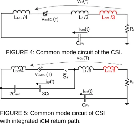
FIGURE 4: Common mode circuit of the CSI.
VCM(T)
LDC/4
+
Lf /3 Lcm/3
VCMZC(T)
S7
irp(t) Rg
2Cmid 3Cf icm(t)
CPV
FIGURE 5: Common mode circuit of CSI with integrated iCM return path.
The common mode circuit of a grid-connected CSI
con-verter is shown in Figure 4. The inductor LCM is a
three-phase common-mode choke that is quite often adopted for electromagnetic interference (EMI) mitigation in off-the-shelf power converters. Because the common mode inductor is connected in series with the parasitic capacitance, an appropriate choice of the parameter must be operated, so that the the switching harmonics are at higher frequency. Having the resonance at lower frequency also allows for an improvement of the power quality, as the common mode circuit could act as a secon-order filter for the common mode voltage harmonics.
In Figure 5 the common mode circuit of the CSI7 with integrated return path is depicted. As can be seen, a switch models the decoupling of the mains and the DC input when the zero vector is applied. As it appears evident from the
cir-cuit, the return path is more effective if the impedance 2Cmid
and 3Cf is lower than the path composed of the inductors and the parasitic capacitance. In fact, the two branches act as a
current divider for the icm.
Although the integrated return path could be applied to any CSI-based topology, it will be shown in the next section that the magnitude of the current flowing through this additional branch could be too high.
there is a circuit formed by only one of the capacitors Cmid and
DC input inductors LDC =2 (due to the presence of the two diodes) and the output CL filter connected as in Fig. 8 together with the grid phase voltages. Since before the application of the zero
vector the voltages across the capacitors Cf are very close to the
grid phase voltages, and the voltage across every Cmid is equal
to VDC =2 a large current can flow in the resulting multi-resonant circuit.
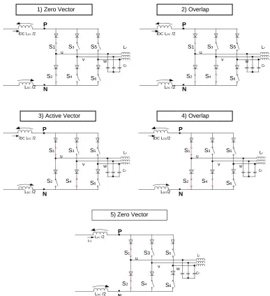
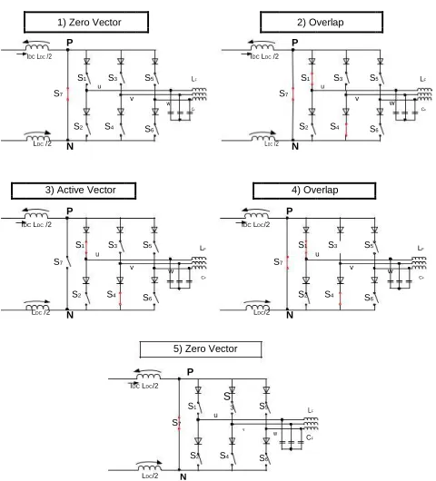
Figure 7 summarizes the switches sequence for the first sextant in case of CSI7 topology with Alternated modula-tion. In case of CSI7 topology, the zero state is applied by turning
on the additional seventh switch S7 with all the other switches off, as shown in Fig.7-1. When introducing the additional return path, the circuit becomes the one depicted in Fig.9. With the CSI7 topology is possible to use the return path, because during the zero state the voltages on filter capacitors don’t change significantly thanks to the discon-nection of the
main full-bridge outputs from Cf capacitors.
Summarizing the issues of the application of the return path, the proposed solution is only viable in case of CSI7 topologies with split input inductors, as the split input induc-tors limit the
value of iRP , as it can be seen by analyzing the common-mode circuit of Fig. 5: in case of a single input in-ductor the equivalent impedance related to LDC disappears.
V. CONSIDERATIONS ON DC SPLIT CAPACITANCE VALUES
The design of the split capacitance must achieve the two objectives:
minimization of the split capacitance to reduce the cost and weight of the converter reduction of the ground leakage current icm
minimization of the current in the return path iRP
These requirements translate into the need of a consider-ably low impedance of the overall return path at the harmonic frequencies of vcmZC . It is important to highlight that the output filter 3Cf is connected in series to the return path, so increasing the value of the split capacitance much above the output filter ones would lead to no additional current reduction.
The common mode impedance icm=vcmZC (j!) of the circuit of Fig. 5 is evaluated. The parameters are listed in TABLE 1 and 2 and the results are shown in Fig. 10.
The same parameters will be used in Section VI for the numerical simulations.
As can be seen from the graph of Fig. 10, values in the range of uF for the return path capacitor allows for a
IV. CLASSIC CSI VS CSI7 BEHAVIOR
Figure 6 shows the switches sequence for the first sextant in case of CSI topology with Alternated modulation. In case of traditional CSI topology, the zero state is applied by turning
on the switches S1 and S2, as shown in Fig.6-1. When
marked attenuation, whereas increasing Cmid above 7 uF,
there is no significant benefits. If Cmid = 0, it means that the CSI converter does not have a return path.
The resulting ground leakage current depends not only on the value of the common mode impedance, but also on the
1) Zero Vector 2) Overlap
P
P
IDCLDC/2 IDCLDC/2
S1 S3 S5 LF S1 S3 S5 LF
u u
v w v w
CF CF
S2 S4 S6 S2 S4 S6
LDC /2 N LDC /2 N
3) Active Vector 4) Overlap
P
P
IDCLDC/2 IDCLDC/2
S1 S3 S5 L
F S1 S3 S5 LF
u u
v w v w
CF CF
S2 S4 S6 S2 S4 S6
LDC /2
N LDC/2
N
5) Zero Vector
P
LDC /2
IDC
S1 S3 S5
LF
u
v w
CF
S2 S4 S6
LDC /2
[image:6.576.93.480.46.470.2]N
FIGURE 6: Switch configuration of Classic CSI during Alternated modulation (sequence covers one half period): (1) zero vector; (2) overlap time; (3) active vector; (4) overlap time; (5) zero vector.
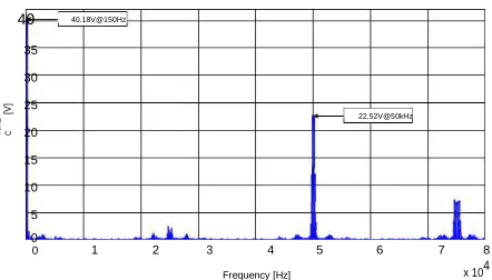
the harmonic component is evaluated in Figs 11 and 12. The main switching harmonics are located at twice the switching frequency 2fs = 50kHz whereas the harmonics introduced by the space vector modulation are at 3fgrid.
As anticipated, the selection of the return path capacitor Cmid must also comply with a limitation of the return path current. The value 7uF represents the optimum of the ca- pacitance size and leakage current minimization, but a lower value could be chosen to limit the magnitude of the return path current iRP .
VI. NUMERICAL SIMULATIONS
All the numerical simulations were carried out in Matlab - PLECS environment considering a string PV source com-posed by a varying number of PV modules, working under MPP condition. The same parameters of TABLE 2 are used,
4
considering 150nF/kWp as the worst case scenario, that translates into 37:5nF for each module.
Two sets of simulations were carried out separately, in order to assess the internal return path solution feasibility in case of different CSI topologies operated with Alternated modulation and to assess the usefulness of the developed
CM equivalent circuits under the definition of VcmZC .
The first set of simulations is aimed at verifying the ef-fectiveness of the proposed internal return path solution at reducing icm value in CSI7 topologies.
For a better modelling of the actual condition, a common mode choke with inductance equal to
Lcm=3x2mH is con-sidered, as explained in Section II. TABLE 1 summarizes all the relevant simulation parame-ters for the power converter simulations.
1) Zero Vector 2) Overlap
P P
IDC LDC /2 IDC LDC /2
S1 S3 S5 LF S1 S3 S5 LF
S7
u
S7
u
v v
w w
CF CF
S2 S4 S6 S2 S4 S6
LDC /2
N LDC /2
N
3) Active Vector 4) Overlap
P P
IDC LDC /2 IDC LDC/2
S1 S3 S5 LF S1 S3 S5 LF
u u
S7 S7
v w v w
CF CF
S2 S4 S
6 S2 S4 S6
LDC /2 N LDC/2 N
5) Zero Vector
P
IDC LDC/2
S1
S
S5
3 LF
u
S7
v
w C
F
S2 S4 S6
LDC/2 N
FIGURE 7: Switch configuration of CSI7 during Alternated modulation (sequence covers one half period): (1) zero vec-tor; (2) overlap time; (3) active vector; (4) overlap time; (5) zero vector.
RLDC /2 P
iPV RCmid iDC LDC/2
Cmid
S1 V+u(t)
VDC U L
f
Vv(t) 0
PV
+
CDC
RCf Vw(t)
Cmid
S2 Cf
+
icm
RLDC /2
LDC/2 N Rg
FIGURE 8: Zero state simplified circuit in case of CSI Topology with integrated iCM return path
[image:7.576.38.278.46.311.2]gies with alternated SVM is carried out in Figure 13 con-sidering the ground leakage current as benchmark: CSI, CSI7 and CSI7 with return path (CSI7+RP). Even with a visual inspection of the waveforms, it is evident that there is a significant benefit changing from a CSI topology to a CSI7 one. CSI7+RP reduces the ground leakage current even further.
Figure 14 shows the phase voltage, grid current and iRP
in the case of CSI7+RP. Return path current iRP results 0.17 A (rms) with a phase current of 1.41 A (rms).
An analysis of the current flowing through the filter capac-itors ICf shows that no great difference exists between the topologies.
The performance comparison considering a different num-ber of PV modules vor the CSI7+RP is reported in Table 4. The increase of the modules implies an increase of the ground
P
iPV iDCLDC/2
Cmid Vu(t)
+
PV VDC S7 Lf Vv(t) 0 +
CDC
Cf Vw(t)
Cmid +
icm
LDC/2 N Rg
FIGURE 9: Zero state simplified circuit in case of CSI7 Topology with integrated iCM return path
20
Cmid =0uF
Cmid =1uF
0 Cmid =2uF
Cmid =3uF
Cmid =4uF
−20 Cmid =5uF
Cmid =6uF Cmid =7uF Ga in [d B]
−40 Cmid =8uF
Cmid =9uF
−60
−80
−100
−120 3 4
2XFS
5
10 10 10
[image:7.576.310.542.248.476.2]Frequency [Hz]
FIGURE 10: Bode Plot of icm=vcmZC (j!) of the CSI7 with integrated return path and 8 panels.
150 100 50 [V] m z c 0 V −50 −100 −150
0.03 0.04 0.05 0.06 0.07 0.08 0.09 0.1 0.02
[image:7.576.39.276.383.476.2]Time [s]
[image:7.576.317.541.567.687.2]40 40.18V@150Hz 35 30 [V ] 25 22.52V@50kHz V cm Z C 20 15 10 5 0
1 2 3 4 5 6 7 8
0
[image:8.576.59.280.57.183.2]Frequency [Hz] x 104
FIGURE 12: FFT of vcmZC with 8 PV modules
TABLE 1: Power Converter Parameters
L
DC
Name Value Unit
2 mH
fS 25 kHz
Tov 2 us
Vgrid (line-to-line) 400 V (rms)
fgrid 50 Hz
Lf 1.4 mH
Lcm 2 mH
Cf 1.5 uF
Rg 4.7 Ohm
Cmid 7 uF
leakage current. It can be seen that this increment is non
linear (more than proportional) because the increase of CP V
reduces the effectiveness of the return path if considering the
same value of Cmid, for different number of modules. In fact,
an increased CP V would reduce the impedance of the grid
return path compared to the internal return path.
From the same table it is possible to see that the RMS value of iRP is proportional to the number of PV modules due to the proportional increase of the
harmonic amplitudes of vcmZC . The value of the return path current is always moderated.
The power losses of the devices in case of 8 PV modules, with and without the return path, were computed in PLECS environment using GW15N120H3 (15A, 1200V) MOSFET and RHRG30120 (30A, 1200V) diodes. The presence of the return path affects in no noticeable manner the power loss.
A second set of simulations was used to assess the pro-posed CM equivalent circuits. The applied method is a two-step process comprising a first step during which the con-verter operation is
simulated with zero CP V and with the disconnection of icm RP.
[image:8.576.327.529.118.324.2]The resulting VcmZC is measured and applied to the equivalent CM circuit (see Fig. 5 by means of a controlled voltage source, in order to obtain the expected
TABLE 2: Nameplate values of the PV module used in simulations.
Name Value Unit
Vmpp 30.3 V
Impp 8.24 A
CP V
single module 37.5 nF
6 5 (a ) [A ] 0
i c m
−5
0.04 0.05 0.06 0.07 0.08 0.09 0.1
0.1
(b
) 0.05 [ A]cm
0
i
−0.05
−0.1
0.04 0.05 0.06 0.07 0.08 0.09 0.1
0.015
(c
)
0.01 0.005 i[A]cm −0.005
0
−0.01 −0.015
0.04 0.05 0.06 0.07 0.08 0.09 0.1
[image:8.576.82.244.218.337.2]Time [s]
FIGURE 13: Simulation results. icm with CSI (a),
CSI7 (b) and CSI7+RP (c). PV source composed
by 4 modules (1kW).
300 200 [A ] 100 1 0 0 *I 0 [V ] V−100 −200 −300
0.02 0.03 0.04 0.05 0.06 0.07 0.08 0.09 0.1
1 0.8 0.6 0.4 (c) 0.2 [A ] 0 i −0.2 −0.4 −0.6 −0.8 −1
0.04 0.05 0.06 0.07 0.08 0.09 0.1
Time [s]
FIGURE 14: Simulation results. Voltage and cur-rent (green trace, x100) and iRP
[image:8.576.330.528.397.600.2]TABLE 3: Simulations results. Performance comparison in case of 4 PV modules
Name Icm [A (rms)] Icf [A (rms)] THD[%] Iu IRP [A (rms)]
CSI 950 3.02 29.18 %
-CSI7 17 2.953 0.978 %
-CSI7+RP 3.5 2.954 0.983 % 0.17
TABLE 4: Simulation results summary with CSI7+RP and CSI7 (only for Icm between brackets)
Name 2 PV modules4 PV modules8 PV modules Unit
P
modules 500 1000 2000 W
CP V 75 150 300 nF
Icm 0.51 (8.3) 3.5 (17) 13.7 (33.5) mA (rms)
IRP 66 170 290 mA (rms)
THD[%] Iu 0.99 0.98 1.08 %
quantities icm and iRP .
A subsequent simulation of the entire converter with the
specified value of CP V and with the connection of the addi-tional return path is then run and the resulting same quantities are compared against each other. Since the additional return path is not technically feasible in case of traditional CSI, all the simulation were carried out only for the CSI7 topology with return path.
Figures 15 and 16 show respectively the iCM waveform and a zoomed-in view of the same: as it can be seen by comparing the results obtained with the actual converter simulation against the ones from the equivalent CM circuit, there is a very good level of agreement.
The same considerations apply in case of figs. 17 and 18,
that show respectively the iRP waveform and a zoomed-in
view of the same. Comparing the results obtained with the actual converter simulation against the ones from the equiv-alent CM circuit results in an excellent level of agreement. The good agreement was obtained despite the neglecting of the power converter behavior during overlap times.
VII. EXPERIMENTAL VALIDATION
A power electronics converter implementing the CSI7 and CSI7 with return path capabilities was realized and the pro-totype is shown in Fig. 19. The goal of the experiments is to evaluate the performance related to the ground leakage current of the different architectures. To decouple the effects of a real grid, the prototype is run in island operation. A balanced resistive load (value 252 Ohm) is used as load and the other experimental parameters match the ones used in
the simulations (TABLE 1). The DC voltage VDC = 120V with
a CP V = 100nF . The reference current is 0:91A) (rms) to
match an equivalent grid voltage Vgrid (line-to-line)= 400V
(rms). Because of the intrinsic boost operation of the CSI, the input voltage must be lower than the line-to-line output voltage.
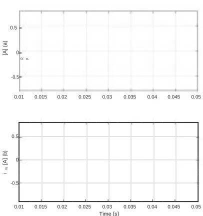
The results are shown in Figures 20 and 21. A phase voltage with the ground leakage current icm and return path current iRP for both solution is shown.
Although several assumptions were made in the simulation part and several non-linear effects of the power converter
10-3
(
)
A
5
[A] 0
CM
I
-5
0.01 0.015 0.02 0.025 0.03 0.035 0.04 0.045 0.05
10-3
(
)
B
5
[A
]
0
CM
I
-5
0.01 0.015 0.02 0.025 0.03 0.035 0.04 0.045 0.05
TIME [S]
FIGURE 15: Waveform comparison of ICM : upper trace - actual converter; lower trace - equivalent CM circuit.
10
-3
5
Actual Converter Equivalent CM Circuit
4.5
[A
] (a)
4
c m
i
3.5
3
0.010.01002 0.01004 0.01006 0.01008 0.0101
Time [s]
FIGURE 16: Zoomed-in waveform comparison of ICM : solid line - actual converter; dashed line - equivalent CM circuit.
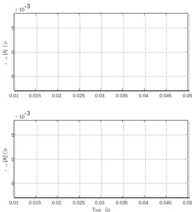
were not modeled, the mitigation of icm from 25:3mA (rms)
to 4:5mA (rms) is confirmed. The current of the return path amounts to 129mA (rms).
In order to obtain a better agreement between simulations
and experiments a better modeling of the power switches Sx
should be carried out. The non linear output capacitance of the power transistors and the junction capacitance of the diodes should be taken into consideration in the simulation of the entire actual converter.
VIII. CONCLUSION
[image:9.576.319.516.58.275.2]photo-0.5
[A
]
(a
)
0
R p
i
-0.5
0.01 0.015 0.02 0.025 0.03 0.035 0.04 0.045 0.05
(b
)
0.5
[A
] 0
Rp
i
-0.5
0.01 0.015 0.02 0.025 0.03 0.035 0.04 0.045 0.05
[image:10.576.53.256.59.275.2]
Time [s]
FIGURE 17: Waveform comparison of IRp: upper trace - actual converter; lower trace - equivalent CM circuit.
0.8
Actual Converter
0.6
Equivalent CM Circuit
(a
)
0.4
[A
]
R p
0.2
i
0
-0.2
0.01 0.01002 0.01004 0.010060.01008
Time [s]
FIGURE 18: Zoomed-in waveform comparison of IRp: solid
line - actual converter; dashed line - equivalent CM circuit.
voltaic applications.
This manuscript carried out an in-depth analysis of the ground leakage current for Current Source Inverters used in grid-connected photovoltaic applications. The proposed ap-proach in order to study and mitigate ground leakage currents in CSI inverter comprises two areas of intervention: first is to provide an internal return path for the common mode current, then suitable CM equivalent circuits are developed to which
apply the definition of VcmZC (common-mode voltage with
zero stray capacitance).
The novelty of the proposed approach relies in the use of two additional capacitors in the DC link whose mid-point is connected to the star point of the CL output filter. The internal return path does not lose its effectiveness even
[image:10.576.297.537.62.240.2]8
[image:10.576.299.549.295.446.2]FIGURE 19: CSI7 power converter prototype
FIGURE 20: Experimental results. CSI7 topology, iu(t) RL (upper trace, 200V/div.), and icm(t) (lower trace, 100mA/div.).
[image:10.576.46.267.340.502.2] [image:10.576.299.550.519.667.2]TABLE 5: Experimental and simulation results comparison (simulation results between brackets)
CSI7 CSI7+RP Unit Icm25.3 (17)4.5 (3.5)mA (rms)
IRP n.a. 129 (170)mA (rms)
when employing only one additional capacitor (of doubled capacitance) connected between the star point of the CL filter and the positive or negative terminal of the DC Source.
This creates an internal return path with lower impedance that prevents the ground leakage current from flowing into the grid.
Thorough study of the different behaviour between tradi-tional CSI and CSI7 topology demonstrated that the internal return path is technologically feasible only for CSI7 topol-ogy,
due to the large iRP in case of traditional CSI topology.
Following the definition of VcmZC , different common-mode equivalent circuits for CSI and CSI7 with additional return path were developed and were validated by means of a two-step simulation process: comparing the relevant waveforms of icm and iRP of the entire converter against the ones of the simplified CM circuit resulted in an excellent agreement.
Thanks to the CSI7 topology, the internal return path is able to significantly reduce the ground leakage current. Specifically, the internal return path requires only the pres-ence of a split input DC
capacitance Cmid and it does not require a dedicated connection to
the grid neutral conductor. In sizing Cmid there is a point of
diminishing returns, after which the attenuation of icm do not
improve significantly even for very large values of Cmid. Simulations and ex-perimental results are in good agreement and show that the proposed solution is able to strongly reduce the ground leakage current. The expected slight increase in power losses does not substantially affect power conversion efficiency of the CSI7 converter. Accurate power losses analysis, together with a more detailed modeling of the power switches non-linear output capacitance will be the subject of future works.
REFERENCES
[1] B. Wu, High-Power Converters and AC Drives, 1st ed. Wiley-IEEE Press, 3 2006.
[2] B. Sahan, A. Vergara, N. Henze, A. Engler, and P. Zacharias, “A single-stage pv module integrated converter based on a low-power current-source inverter,” IEEE Trans. Ind. Electron., vol. 55, no. 7, pp. 2602–2609, 2008.
[3] B. Sahan, S. Araujo, C. Noding, and P. Zacharias, “Comparative evaluation of three-phase current source inverters for grid interfacing of distributed and renewable energy systems,” IEEE Trans. Power Electron., vol. 26, no. 8, pp. 2304–2318, Aug 2011. [4] D. Chen, J. Jiang, Y. Qiu, J. Zhang, and F. Huang, “Single-stage
three-phase current-source photovoltaic grid-connected inverter high voltage transmission ratio,” IEEE Transactions on Power Electronics, vol. 32, no. 10, pp. 7591–7601, Oct 2017.
[5] A. Ciocia, V. Cocina, P. Colella, P. D. Leo, E. Pons, F. Spertino, and
R. Tommasini, “Ground currents in a photovoltaic power plant: Theoretical approach and experimental tests,” in 2017 IEEE Manchester PowerTech, June 2017, pp. 1–6.
[6] D. Meneses, F. Blaabjerg, Ã. GarcÃa, and J. A. Cobos, “Review and
comparison of step-up transformerless topologies for photovoltaic ac-
module application,” IEEE Transactions on Power Electronics, vol. 28, no. 6, pp. 2649–2663, June 2013.
[7] L. Concari, D. Barater, A. Toscani, G. Franceschini, G. Buticchi, M. Lis-erre, and H. Zhang, “Assessment of efficiency and reliability of wide band-gap based h8 inverter in electric vehicle applications,” MDPI Energies, 2019.
[8] D. Dong, F. Luo, D. Boroyevich, and P. Mattavelli, “Leakage current
reduction in a single-phase bidirectional ac-dc full-bridge inverter,” IEEE Trans. Power Electron., vol. 27, no. 10, pp. 4281 –4291, Oct. 2012. [9] E. Lorenzani, F. Immovilli, G. Migliazza, M. Frigieri, C. Bianchini, and M.
Davoli, “Csi7: A modified three-phase current-source inverter for modular photovoltaic applications,” IEEE Transactions on Industrial
Electronics, vol. 64, no. 7, pp. 5449–5459, July 2017.
[10] E. Lorenzani, G. Migliazza, F. Immovilli, and G. Buticchi, “Single-stage three-phase current-source photovoltaic grid-connected inverter high volt-age transmission ratio,” Chinese Journal of Electrical Engineering, June 2019.
[11] E. Lorenzani, G. Migliazza, and F. Immovilli, “Ground leakage current mitigation for three-phase current source inverters,” in 2018 IEEE Energy Conversion Congress and Exposition, Sept 2018. [12] G. Buticchi, D. Barater, E. Lorenzani, and G. Franceschini, “Digital
control of actual grid-connected converters for ground leakage current reduction in pv transformerless systems,” IEEE Trans. Ind. Informat., vol. 8, no. 3, pp. 563–572, Aug 2012.
[13] J. Rodriguez, L. Moran, J. Pontt, R. Osorio, and S. Kouro, “Modeling and analysis of common-mode voltages generated in medium voltage pwm-csi drives,” IEEE Transactions on Power Electronics, vol. 18, no. 3, pp. 873–879, May 2003.
EMILIO LORENZANI (S’03-M’07-SM’18) was born in Parma, Italy, in 1976. He obtained his M.S. degree in Electronic Engineering in 2002 and his Ph.D. in Information Technologies in 2006, both at the University of Parma, Italy. Since 2011 he has been at the Department of Science and Engineering Methods at the University of Modena and Reggio Emilia, where he is currently an As-sociate Professor of Electric Machines and Drives. His research activity is mainly focused on power
electronics for renewable energy resources, electric drives and electric motor diagnostics. He is the author or coauthor of more than 70 technical papers, and holds five industrial patents.
FABIO IMMOVILLI (S’08-M’11-SM’19) re-ceived the M.S. degree and the Ph.D. in Mecha-tronic Engineering at the University of Modena and Reggio Emilia, Italy, in 2006 and 2011 respec-tively. In 2009, he was a Visiting Scholar at the Power Electronics, Machines and Control Group of the University of Nottingham, Nottingham, UK. Since November 2016 he is an Assistant Profes-sor of Electric Converters, Machines and Drives at the Department of Sciences and Methods for
Engineering, University of Modena and Reggio Emilia, Italy. His research interests include electric machine condition monitoring, electric power con-verters, machines for energy conversion from renewable energy sources and thermoacoustics. He holds two international industrial patents.
CHRIS GERADA received a PhD degree in nu-merical modelling of electrical machines from the University of Nottingham, Nottingham, UK, in 2005. He subsequently worked as a re-searcher at the University of Nottingham on high-performance electrical drives and on the design and modelling of
electromagnetic actuators for aerospace
applications. He was appointed Lecturer in electrical machines in 2008, Associate Pro-fessor in 2011, and Professor in 2013. His core
research interests include the design and modelling of high-performance electric drives and machines. Prof. Gerada is an Associate Editor of the IEEE Transaction on Industry Applications. He has secured major industrial, European and UK grants, authored more than 200 papers and has been awarded a Royal Academy of Engineering Research Chair to consolidate research in the field.
HE ZHANG received his B.Eng. degree from Zhejiang University, China, in 2002. He obtained the MSc. and Ph.D. degree in electrical machines from The University of Nottingham, UK, in 2004 and 2009 respectively. After this he worked as Research Fellow at the University. He moved to University of Nottingham Ningbo China and be promoted to Senior Research Fellow in 2014 and Principal Research Fellow in 2016. Currently he is the director of Nottingham Electrification Centre
(NEC) within the Power electronics, Machines and Control research group in University Of Nottingham. His research interests include high performance electric machines and drives for transport electrification.
10
GIAMPAOLO BUTICCHI (S’10-M’13-SM’17)
received the Master degree in Electronic Engi-neering in 2009 and the Ph.D degree in Informa-tion Technologies in 2013 from the University of Parma, Italy. In 2012 he was visiting researcher at The University of Nottingham, UK. Between 2014 and 2017 he was a post-doctoral researcher at the University of Kiel, Germany. He is now Associate Professor in Electrical Engineering at The University of Nottingham Ningbo China. His