Fabrication of diffraction-encoded micro-particles using
nano-imprint lithography
Shahanara Banu
1, Sam Birtwell
2, Gerasim Galitonov
2, Yifang Chen
4, Nikolay
Zheludev
2and Hywel Morgan
31School of Chemistry, 2Optoelectronics Research Centre, 3School of Electronics and Computer Science,
University of Southampton, Highfield, Southampton, SO17 1BJ, UK. 4Rutherford Appleton Laboratory, Chilton, Didcot, Oxon OX11 0QX, UK
E-mail: [email protected], [email protected]
Abstract
A nano-imprint lithography technique is described for fabrication of optically encoded micro-particles (diffractive barcodes). The micro-particles are fabricated from SU8 – a material which can be processed lithographically, and which can be used for attachment of molecular tags. The barcodes are identified by their unique diffraction patterns.
1. Introduction
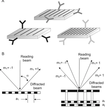
Advances in genomics, proteomics, combinatorial chemistry and high throughput screening have led to the development of techniques for multiplexed analysis. In particular, bead-based multiplexed chemical analysis offers a number of advantages over conventional array-based approaches. Bead-based analysis uses solid micrometer sized beads as platforms for chemical or biochemical reactions or assays. In order to simultaneously perform more than one assay, the beads must carry a unique identifier indicative of the molecule on its surface, i.e. a bar-code, as shown in figure 1A. A number of approaches have been developed for bar-coding particles, mostly based on spectral or spatial encoding [1-4]. For example, by fabricating particles containing several different fluorescent quantum dots with discrete emission intensities it is possible to produce several hundred unique codes [5,6]. However, encoding with fluorescence has many problems; not least that fluorescence is one of the most common techniques used to indicate that a chemical reaction has taken place on a bead. We have recently developed a new approach to bar-coding particles based on the fabrication of micron sized diffractive elements [7]. The “code” is read by measuring the spatial distribution of light diffracted by a pattern on the surface of a bead. In the simplest implementation, the pattern on the particle is a miniature diffraction grating (a few micrometres in size), where information is encoded in the pitch of the grating, a. When the grating is illuminated with light at wavelength λ, for example at normal incidence, a series of diffracted beams at angles αare created, according to the equation a sinα = mλ, where m is an integer known as the order of the diffracted beam. Measurement of the first order (m = 1) diffracted beam position (with respect to the zero order) gives direct information about the pitch a. More than one grating pitch can be superimposed on a single particle to increase the encoding capacity of this technique. The principle is shown in figure 1B. Using this technique, we estimate that approximately 109 unique codes can be created from 5 superimposed gratings on a 50 μm long particle [7].
negative resist [8-11]. SU8 is chemically robust, and can be processed using conventional photolithography to produce a wide range of high aspect ratio structures. The resist is commercially available in different formulations, and can be processed by spinning to produce films in the range of 1-100 μm thickness, depending on the viscosity of the original solution and the spin speed [8-10]. SU8 contains a photo-acid which, when exposed to light (wavelength 365nm), initiates the polymerization of the epoxy groups. SU8 has been microfabricated into a range of microstructures, including microfluidic devices [12-14], moulds and masters for microembossing [15,16], probes for microscopy [17], and biosensors [18]. Because of its outstanding performance in microfabrication, optical transparency in the visible range, and excellent physical and chemical stability, SU8 has recently attracted attention for use in bioanalytical applications as a support material for the direct attachment of biomolecules [19-24]. After micro fabrication, residual epoxy groups can be used for surface functionalization [19,20]. We recently demonstrated that SU8 can be used to manufacture micron-sized blocks of material (i.e. beads) and that these blocks can be further processed using conventional multistep solid-state synthesis of oligonucleotides and peptides [25]. Although SU8 can be processed using optical lithography to produce features of the order of the wavelength of light, this resolution is not sufficient to produce high quality multiply superimposed diffraction gratings. We have therefore developed a fabrication method which is based on nano-imprint lithography (NIL). NIL is a technique that can replicate micro- and nano-scale patterns with high fidelity, and is beginning to have a significant impact in micro and nanotechnology [6]. It is a relatively simple process and may form part of a suite of new technologies for the mass production of nano-sized patterns.
In conventional nano-imprint lithography, a high resolution stamp is fabricated in a hard material such as Silicon or fused Silica using a combination of electron beam lithography and dry etching. The generic process, figure 2 shows how the stamp is imprinted into a soft polymer to produce a high quality replica. The process can be repeated many times, providing material transfer from the substrate to the master is minimized using an anti-stick coating.
In this paper, we describe a process for nano-imprinting of SU8 microparticles manufactured by photolithography and demonstrate that well resolved optical diffraction gratings can be manufactured, with high fidelity and high aspect ratio. The method is performed at low temperature, with low pressure and produces excellent uniformity in the quality of the resulting imprinted structures.
2.Experimental
2.1 Fabrication of the stamps
The embossing stamps were made in sizes of 2 x 2 mm, each containing arrays of gratings 50 µm x 50 µm, as shown in figure 3B. These stamps were used to imprint barcodes onto flat sections of SU8 for characterisation. The same stamps were used to imprint SU8 bars for fabrication of encoded particles.
2.2 Photolithography and nano-imprinting
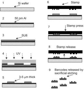
The encoded bars were fabricated according to a two step lithographic process, followed by hot embossing as shown in figure 4. In the first step individual bars were fabricated from SU-8; these were subsequently nano-imprinted using the master stamp to produce the diffractive bar-codes. The diffraction gratings were imprinted into the particles in such a way that it was possible to produce several million particles.
The SU8 microbars were fabricated on Si wafers (525±25 µm Si-Mat Silicon Materials, Germany) by photolithography using SU8-5 (figure 4, steps 1 – 5). In order to ensure easy release of the bars from the substrate, the Si wafers were first covered with a 50 nm thick Al sacrificial layer. Full details of the fabrication of the SU8 bars can be found in a previous publication [25]. The final thickness of the SU8 bars could be adjusted by varying the thickness of the SU-8 layer, which was typically in the range 3-10 µm. After coating the wafer with SU8, followed by baking, the wafer was exposed to 365 nm light (I-line) through a mask, using a MA6 (SUS Microtech) mask aligner, with an optimized exposure dose in the range 60-200 mJ cm-2, depending on the thickness of the SU8. After exposure, the wafers were baked at 65 °C for 1-3 minutes, and the temperature was then increased for 2-6 minutes at 4 °C per minute, to 95 °C. The wafers were developed in PGMEA EC solvent (polypropylene-glycol-methyl-ether-acetate, Chestech Ltd, UK.) for 2 minutes with agitation, then thoroughly rinsed with isopropyl alcohol and blow dried. If required the bars could be released a this stage by etching the Al sacrificial layer. This was achieved by sonicating the wafers in TMAH (Micorposit MF-319, Chestech Ltd, UK) at room temperature for 10 minutes.
In order to ensure complete detachment of the stamp after imprinting [11], the stamp was coated with a monolayer of anti-stick agent, Trichloro (1H, 1H, 2H, 2H-perfluorooctyl) silane. The stamp was soaked in a solution of 1-2% silane in ethanol for 30 minutes, rinsed with ethanol and baked in an oven at 120 °C for 30 minutes.
As shown in the SEM of the SiC master, a superimposed diffraction grating has many lines of different pitch and width (figure 4A). Imprinting was performed by pressing the master onto a 4 x 4mm area of wafer containing pre-fabricated SU8 bars (figure 5) or films, both with thicknesses in the range 3-5 µm. A home-made press was used, based on a screw clamp arrangement, in which the pressure was adjusted using a torque-wrench. The applied force was calculated from the torque using a standard method for calculating the clamping force due to a screw. The imprinting force was distributed as homogeneously as possible using a piece of PDMS sheet between the stamp and the pressure plate. The stamp was aligned by eye with the substrate and then the assembly was pre-baked. The required force was applied using the torque-wrench, and the system again baked. In order to optimise the imprinting, a range of forces and temperatures were tested. Forces were in the range 230-690 N (over the 2 x 2 mm stamp) and the baking temperature was ramped from 50-100 °C at 4 °C min-1 for 5 minutes.
3. Results and Discussions
During imprinting, it was noted that many of the bars did not adhere to the Al layer covering the Si wafer and became adhered to the master. The adhesion of the SU8 to the Al layer was partly improved using universal Ti primer, but bars continued to detach from the substrate during imprinting. An additional hard baking step was adopted which increased the adhesion of the SU8 and enabled imprinting without detachment or damage of the bars. The optimised imprint process was performed with the substrate held at a temperature of 85 °C for 5 minutes, with an imprint pressure that depended on the aspect ratio of the embossing master. Above the glass transition temperature the SU8 is able to flow out of the imprinting region [26]. Therefore, arrays of small gratings are preferable to a large continuous pattern, where the flow of the SU8 is constricted. After optimisation, it was found that stamps containing an array of 50 μm x 50 μm gratings produced embossed features with the best quality.
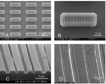
In order to characterize the imprinted patterns, gratings of 50 x 50 μm were fabricated in flat SU8 films. With an imprinting force of 690 N, high quality gratings with high aspect ratio (figure 5C and 5D) were obtained from a master, in this case with feature depth of 650 nm. The optical properties of these nano-embossed patterns were measured using the experimental system shown in figure 6. A helium-neon laser (wavelength λ = 633 nm) was focused by a lens (focal length f = 100 mm) onto a sample plate containing a thin film of SU8 into which 50 x 50 μm barcodes had been embossed. The resulting diffraction pattern was projected onto a CCD camera. The diffraction images recorded for an example set of 5 barcodes, each with two superimposed gratings, are shown in figure 7. In this figure, one of the grating pitches remains constant, whilst the pitch of the second increases from barcode A to E. The first order diffracted beams, which constitute the code, are clearly visible and well defined. The figure shows that the code can be easily read by measuring the positions of the first order spots relative to the zero-order beam. Reading of the barcodes is accomplished automatically using this setup, with the CCD camera connected to a PC running dedicated software. The diffraction patterns obtained from the nano-imprinted codes, as shown in figure 7 A-E, are of high quality and appear almost identical to those obtained using classical gratings made from metal on glass by high resolution e-beam direct write [7] (examples shown in figure 7F-J).
4. Conclusions
We have demonstrated a low cost imprinting technique, based on hot embossing nano-patterns into photo-lithographically processed micrometre sized SU8 bars. Using this technique, large numbers of microparticles can be produced, each set with a unique bar-code. The codes are defined by the pitch of superimposed diffraction gratings produced in the particle surface. The particles produced by this method can be further processed for chemical or biochemical attachment. The embossed diffraction grating has a high aspect ratio, and shows excellent fidelity to the original master. Nanometer resolution is obtained, giving high quality diffraction patterns which are indistinguishable from metal on glass gratings fabricated by electron-beam direct write. The technique uses a simple home-made imprinting tool, the structures do not require UV exposure during the embossing step and the stamps are not contaminated by un-crosslinked viscous polymer, which is one of the main limitations of nano-imprinting [27].
Acknowledgements
The authors acknowledge the financial support of the UK Engineering and Physical Sciences Research Council and the Basic Technology Research Program of the UK Research Councils.
References
[2] Dejneka M J, Streltsov A, Pal S, Frutos A G, Powell C L, Yost K, Yuen P K, Muller U, and Lahiri J 2003 PNAS100 389-393
[3] Seydack M 2005 Biosens. Bioelectron.20 2454-2469
[4] Su X, Zhang J, Sun L, Koo T, Chan S, Sundararajan N, Yamakawa M and Berlin A 2005
Nano Lett.5 49-54
[5] Jaiswal J K and Simon S M 2004 Trends Cell Biol.14 497-504
[6] Mattheakis L C, Dias J M, Choi Y, Gong J, Bruchez M P, Liu J and Wang E 2004 Anal. Biochem.327 200-208
[7] Galitonov G S, Birtwell S W, Zheludev N I and Morgan, H 2006 Opt. Express 14 1382-1387
[8] Shaw J M, Gelorme J D, LaBianca N C, Conley W E and Holmes S J 1997 IBM J. Res. Dev.41 81-94
[9] Lorenz H, Despont M, Fahrni N, Brugger J, Vettiger P and Renaud P 1998 Sens. Actuator A-Phys.64 33-39
[10] Lorenz H, Despont M, Fahrni N, LaBianca N, Renaud P and Vettiger P 1997 J. Micromech. Microeng.7 121-124
[11] http://microchem.com/products
[12] Carlier J, Arscott S, Thomy V, Fourier J C, Caron F, Camart J C, Druon C and Taburier P 2004 J. Micromech. Microeng.14 610-624
[13] Svasek P, Svasek E, Lendl B and Vellekop M 2004 Sens. Actuators A.115 591-599,. [14] Ribeiro J C, Minas G, Turmezei P, Wolffenbuttel R F and Correia J H 2005 Sens. Actuator A-Phys.123-24 77-81
[15] Hyouk I and Ajmera P K 2003 J. Micromech. Microeng.13 816-821
[16] Koerner T, Brown L, Xie R X and Oleschuk R D 2005 Sens. Actuator B-Chem.107 632-639
[17] Lee J, Shin H, Kim S, Hong S, Chung J, Park H and Moon J 2003 Jpn. J. Appl. Phys. Part 2 - Lett.42 L1171-L1174
[18] Chang-Yen D A and Gale B K 2003 Lab Chip3 297-301
[19] Evans M, Sewter C and Hill E 2003 Assay Drug Dev. Technol.1 199-207
[20] Kaye P H and Tracey M C 1997 (University of Hertfordshire, UK) UK Patent Number GB2306484
[21] Preininger C and Sauer U 2003 Sens. Actuator B-Chem.90 98-103
[22] Preininger C, Bodrossy L, Sauer U, Pichler R and Weilharter A 2004 Anal. Biochem.330 29-36
[23] Preininger C, Sauer U, Dayteg J and Pichler R 2005 Bioelectrochemistry67 155-162 [24] Marie R, Schmid S, Johansson A, Ejsing L, Nordstrom M, Hafliger D, Christensen C B V, Boisen A and Dufva M 2006 Biosens. Bioelect.21 1327-1332
[25] Cavalli G, Banu S, Martins H, Ranasinghe R T, Neylon C, Morgan H, Bradley M and Roach P 2006J. Comb. Chem., xx, xx-xx (in the press)
[26] Guo L J 2004 J. Phys. D: Appl. Phys. 37 R123-R141 [27] Cheng X and Guo L J 2004 Microelec. Eng. 71 288-293
Figure 2. Schematic of a generic imprint process. A patterned master (stamp) is brought into contact with a soft polymer. After releasing, a copy of the master pattern is imprinted into the surface of the polymer.
Figure 3. SEM images of a nano-embossing master. The high aspect ratio and uniformity of the structures can be seen (A), together with the multiple periods evident in a superimposed grating pattern. Single grating patterns are 50 μm square (B), with many such patterns in an array over a 2 x 2mm area.
(6 – 8), with baking during step 7. Finally, the patterned bars are released by etching away the Al layer.
Figure 5. An array of nano-imprinted microbars (A), with a high quality diffraction grating pattern (B) reproduced on the surface. The depth of the features (C) and uniformity of the profile (C & D) are shown here in patterns imprinted into flat SU8 films.
[image:8.595.90.392.530.654.2]