International Journal of Innovative Technology and Exploring Engineering (IJITEE) ISSN: 2278-3075,Volume-8 Issue-6, April 2019
Abstract: In this work, we have discussed a new approach in designing the phase-locked loop (PLL), the proposed circuit is designed with the GDI cell-based PFD, charge pump and low pass filter. For frequency matching and for larger locking state, the design used as D flipflop from the TSMC library. It is used as frequency synthesizers and divides the incoming frequency by 2.This design uses 5 stage current starved voltage control oscillator (CS-VCO). The designed PFD is free from the dead zone issue and it is suitable for the low power applications. the designed PLL works for an average frequency range of 8 GHz and its offset frequency is targeted at 1GHz.This PLL model has low phase noise of -112 dBc/Hz at 1 Mhz frequency which is quite standard and the power consumption of the circuit is 8 µW. The entire work is simulated using Cadence Virtuoso 45 nm Technology.
Index Terms: Charge pump, FD, PLL. PFD, Phase locked loop
I. INTRODUCTION
Phase locked loop (PLL) is nowadays have become one of the most important parameters of the modern electronics and communication circuits and of their designs. Work on PLL has started in the late thirties of the 19th century as a part of rapid growth in the IC technologies. Going by the history of the phase locked loop, the early PLL based IC was introduced in some mid-range of 1960-1965. Which was mainly designed using with the help of analog component .now a day since more focus on work is over the integrated circuit, hence the requirement is on the construction of phase locked loop to achieve better results with a better reliable status. Nowadays entire PLL is in general integrated into a single chipset giving a major economic boost. Still, this area is widely considered for research and development because of its low power, high radio frequency aspect and it's also very widely used in low power, high-frequency range MOSFET application. Earlier research was mostly based on the outlines and working of phase locked loop, now research in this field is mostly dedicated towards its application and how we can fit it in modern electronics designs. The widest application of the phase locked loop is in frequency synthesis and in generating high radio frequency. Since a crystal oscillator cannot generate high frequency and hence here, PLL comes into the picture. A phase-locked loop since it comes under the RF
Revised Manuscript Received on April 07, 2019.
Shubham, Department of Micro and Nanoelectronics, School of Electronics Engineering , Vellore Institute of Technology, Vellore -632014, Tamilnadu , India
Sakthivel R, Department of Micro and Nanoelectronics, School of Electronics Engineering , Vellore Institute of Technology , Vellore -632014, Tamilnadu , India
signal domain, it is expected that its design will generate a very high-frequency range, will consume less power and the output will have less jitter and less phase noise. Since that phase locked loop is not just a single circuit but it consists of a whole set of sub circuit it also poses challenges in terms of designing aspect and maintaining the high-frequency parameter.
II. PLLARCHITECTURES&WORKING A PLL [4] is close feedback circuit system. It mostly compares the output frequency signal to the input frequency signal through PFD. Entire working is explained in the following sections. Generally, we can also say that an RFIC circuit consists of several subcircuits. Together functioning of all these circuits is called as the functional phase locked loop. In Fig.1we have shown a basic working model of PLL.
PFD CHARGE-PUMP LPF VCO
FREQ.DIVIDER (DIVIDED BY 2)
Vref
UP
DN UP
DN
Vcntrl
Ipump
Divider_freq
Vvco
Phase locked loop block
Fvco
Fvco/2
Fig1. PLL Block Diagram
In a PLL. There are 5 working sub circuit which are 1. Phase Frequency Detector
2. Charge Pump 3. Low Pass Filter
4. Voltage Controlled Oscillator (Vco) 5. Frequency Divider (Fd).
The primary working of PLL is to compare the output frequency of the VCO is to the input reference frequency. This comparison is done by the phase frequency divider and it generates an error signal (UP, DOWN) as its output which is fed as the input of Charge pump. This charge pump combines its output and generates a single charge current (Ipdi) which is constant in magnitude but it differs in the polarity. This positive or negative polarity of the circuit is entirely dependent on the PFD [1] output.
Low Power, Low Phase Noise Based Phase
Locked Loop and Its Design Implementations
This current input is then passed as an input of loop filter which acts like a low pass filter (LPF). It generates a control voltage at the output, this output is used to drive the VCO circuit. The output of the VCO is then passed to the frequency divider, which divides the frequency to match the lock range and then this input is passed back as the feedback input to PFD to complete the closed loop.
A. Phase Frequency Detector
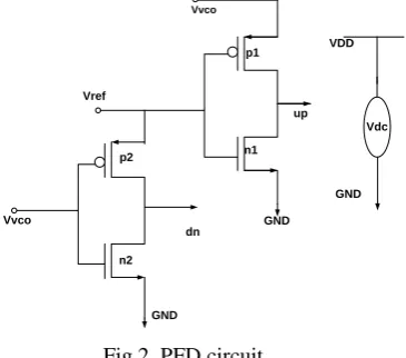
A PFD [2] is mostly built with the memory element such as D flip-flop using a state machine table for verifying the output. The very basic architecture of the phase frequency detector is shown in fig.2 and it is implemented in CMOS logic based D flip-flop. [7] This was very widely and vastly used PFD circuitry but it has equally more drawbacks like of high power consumption, pulling up and down the issue of nodes at high frequencies, and the main and major issue was this circuit had "dead zone" issue.[3] Furthermore since PFD has the main work of detecting phase and frequency error. There was very simple and logic gates based topology was there like XOR gate based PFD, NAND gate based PFD, NOR gate based PFD but these also had issues regarding dead zone, power consumption, and limited speed.to solve these problems we designed GDI cell-based PFD is almost similar to the functioning of the normal and conventional phase frequency detector. This PFD is based on two GDI cell, i.e. here we have used only four transistors in comparison of earlier 15T or 10T [8] based approach. Here we have again applied two clock pulse as the input as reference frequency clock and the frequency of the output of VCO clock. Again like others, two output is up and down.The verification of output can be done as follows if the reference frequency leads VCO output frequency then UP will go high for that time interval and if VCO output leads the reference frequency, then, in that case, down will go high, at the same frequency of inputs, the output will go down. That is at this time both of the UP and DOWN will be zero. Fig 2. Shown is the PFD based on GDI cell.
Vdc Vref
Vvco
dn
up p1
n1 p2
n2
VDD
GND
GND
GND Vvco
Fig 2. PFD circuit
[image:2.595.86.269.565.726.2]The parameters of PFD is shown in table I.
Table I. Parameters used in GDI cell-based PFD
Parameter GDI_PFD
1.Technology 45nm
2.No Of Transistor 04
3.Power 25 uW
4.Dead Zone Free
5.Supply Power 1.2 V
B. Charge Pump and LPF
A charge pump (CP) [4] is basically functioned as a dc to dc converter. It is placed after PFD in PLL construction hierarchy. The main function of the charge pump is to deliver a current output and hence it is also sometimes referred to as the current synthesizers. It also generates a voltage which is used to drive the VCO circuit. The output changes in VCO is entirely dependent on the output generated by the CP circuit. The two output up and down generated by the PFD is supplied to Charge pump circuit as its input and it generates a single output which is fed as the input of the loop filter. CP always produce a current (Ipdi) as its output. This current always has the same output but its polarity varies. This change of polarity entirely depends on its input that is on up and down of the PFD. The mathematical expressions are given as
(1.) &
(Amps/radian) (2.)
We can also write phase difference as
= (3.)
If PLL is in the lock then phase difference will be 0.
Low Pass Filter – the passive loop filter or in the circuit we preferred it calling as low pass filter because of its functioning. It is used to generate the charge pump output which is a charge pump current back into the control voltage. This output voltage is going to be the driving voltage of VCO and the oscillations frequency of the VCO will entirely dependent on the control voltage. In Fig 3.. We have shown the circuit of the Charge pump and Low pass filter.
International Journal of Innovative Technology and Exploring Engineering (IJITEE) ISSN: 2278-3075,Volume-8 Issue-6, April 2019
Table II. Parameters used in design of charge pump
Parameter Values
1.Technology 45nm CADENCE
2.Power supply 1.2 V
3.C1,C2 15 pF
4.Ipump 600 u
5.R1 10K
vdd
Ipump
inv up
down
Ipump
gnd M1
M2
Ipdi VinVCO
C1
R1 C2 Ipdi
Fig.3 Charge pump with low pass filter.
C. Voltage Controlled Oscillator Design and Working.
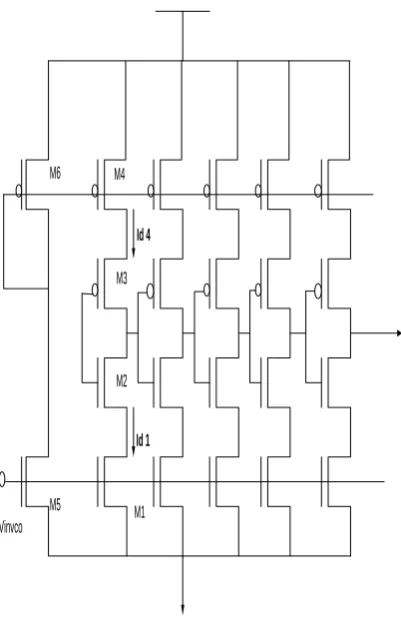
In our design of PLL, We designed the PLL using a very popular scheme that is current starved ring oscillator (CSVCO) [3]. No of inverters we used is this design is 5. Basically, a VCO [5] is termed as a circuit whose oscillation frequency is controlled by an input voltage provided to it. Design of VCO is a cascaded set of inverters. The final output of the inverter is feedbacked to the design circuit.
Mostly range of a CS-VCO is in GHz but it varies depending on the control voltage and offset frequencies provided by the designer.
The Oscillation frequency of the VCO depends not just on the control voltage but also on the parameter such as
1. Number of stages 2. Delay of inverter
3. Total Capacitance of the circuit. 4. Power supply
5. Input voltage supply 6. Drain current.
We can also say that the
(3.)
Where N = no of stage and D is a delay
If we will increase the number of inverters then oscillation frequencies will be reduced. The circuit of a CS-VCO is shown in Fig 4.
Vinvco M1
M2 M3 M4
M5 M6
[image:3.595.61.271.67.376.2]Id 1 Id 4
Fig 4. 5 stage CS-VCO circuit.
D. Frequency Divider
Frequency Divider (FD) [7] block completes the PLL circuit and as well as the frequency synthesizer circuit. It is used in the PLL circuitry to scale down the output frequency.Frequency Divider is positioned in between the output feedback path and hence it completes the closed loop path of the PLL circuit. The function of the Frequency divider is to divide the output frequency by "n". The VCO output frequency has to be scaled down before feed backed into the circuit to match the locking range. Most commonly used circuit in frequency divider is the D flip flop based architecture. There are practical reasons to use the D flip flop as a frequency divider in the PLL circuit.
III. SIMULATIONRESULTS
A.Output of PFD
[image:4.595.53.286.62.271.2]
Fig.5 Output of PFD
B.Output of charge pump-loop pass filter Control voltage = 3.84 V.
Hence this voltage will be used to drive the VCO circuit.
Fig 6. Output of the Charge Pump C. PLL waveforms
Fig 7. Waveform of PLL in Locked state
Oscillation frequency = 8 GHz
Fdiv = 3.95 GHz. Power supply = 1.2 V
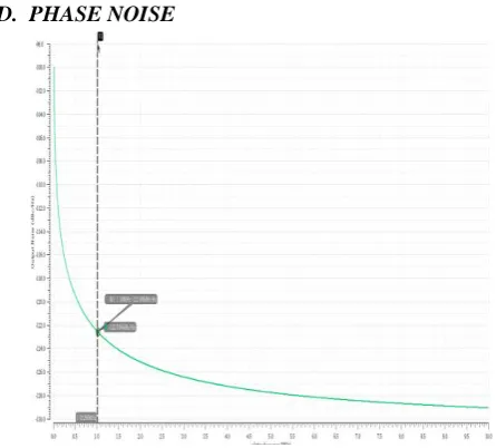
D. PHASE NOISE
Fig 8. Phase noise of designed PLL
At standard 1 MHz frequency, the phase noise of the circuit is -112 dB/Hz. Which is quite less & standard.
IV. DISCUSSIONOFSIMULATEDRESULTS
The simulation results reported at the proposed PLL provides a low phase noise of - 112 dBc/Hz at 1 MHz offset frequency and the power consumption of 8 µW. The power
consumption of this model is quite less and a better phase noise value has been achieved. Locking range of this PLL is after 20 ns Tstab time till 8 GHz. Table III shows the final simulated values of the PLL.
Table III. Final values of designed PLL
Parameters Values
1.Technology 45nm
2.Power supply 1.2 V
3.Pll frequency 7.9 GHz
4.Avg power pll 8 µW.
5.Phase noise -112 dB@1MHz
6.Control voltage 3.84 V
[image:4.595.309.532.90.291.2]International Journal of Innovative Technology and Exploring Engineering (IJITEE) ISSN: 2278-3075,Volume-8 Issue-6, April 2019
V. CONCLUSION
This work came with designing a PLL with VCO, 40 MHz – 1000 MHz, ultra-low phase noise -110 dBc/Hz and very low RMS jitter of 180 fs.The circuit has been designed, constructed using cadence virtuoso and simulations was performed by spectre with the model file of 45 nm Technology provided by TSMC. The proposed circuit applies GDI techniques for PFD model which leads to the low power consumption of the circuit. The average frequency of 8 GHz and phase noise of -112 dBc/Hz was achieved. Since the phase noise is very less it could be used in low power based applications. The designed charge pump had also few edges over another model such as Increased output voltage swing. Our main aim was to achieve low power consumption of the circuit which we have observed that this PLL circuit has consumed a power supply of 8 µW.
REFERENCES
1. Mansuri, M., Liu, D., Yang and C.-K.K., "Fast frequency acquisition phase-frequency detectors for Gsamples/s phase-locked loops” Solid-State Circuits, IEEE Journal of, vol.37, no.10, pp.1331,1334, Oct 2002.
2. Ismail, N.M.H. and Othman, M., "CMOS phase frequency detector for high-speed applications" Microelectronics (ICM), International Conference on, vol., no., pp.201,204, 19-22 Dec. 2009.
3. Rout, P.K., Panda, B.P., Acharya, D.P. and Panda, G. (2014) ‘Analysis and design of 1 GHz PLL for fast phase and frequency acquisition’,Int. J. Signal and Imaging Systems Engineering, Vol. 7, No. 1, pp.30–37. 4. Best, R.E. (2003) ‘Phase Locked Loops design, simulation and
applications’, 5th ed., McGraw-Hill Publication. Symposium on, vol., no., pp.1342,1345 Vol. 2, 7-10 Aug. 2005.
5. B. P. Panda, p. K. Rout, d. P. Acharya and g. Panda “Design of a novel current starved VCO via constrained geometric programming” april 12-14 2011 international symposium on devices mems intelligent systems communications 2011.
6. K. Arshak, O. Abubaker, and E. Jafer, “Design and Simulation Difference Types CMOS Phase Frequency Detector for High Speed and Low Jitter PLL”, proceedings of 5th IEEE International Caracas Conference on Devices, Circuits, and Systems, Dominican Republic, Vol. 1, Nov.3-5, pp.188-191, 2004.
7. Baker, R.J., Li, H.W. and Boyce, D.E. (2002) ‘CMOS Circuit Design, Layout, and Simulation’, IEEE Press Series on Microelectronic Systems, Vol. 19, pp.373–417.
8. Abdul Majeed, K.K. and Binsu J. Kailath, “Low power, High Frequency, Free Dead Zone PFD for a PLL Design”, IEEE 2013. 9. Baker, R.J., Li, H.W. and Boyce, D.E. (2002) ‘CMOS Circuit Design,
Layout, and Simulation’, IEEE Press Series on Microelectronic Systems, Vol. 19, pp.373–417.
AUTHORSPROFILE
Shubham, currently doing his M.Tech in VLSI design (2017-19), Vellore Institute of Technology. Vellore. He has done projects on low power IC & in memory design .The author has completed his B.E in Electronics and Communications from Visvesvaraya Technological University, Bengaluru in 2016.Shubham has successfully delivered a conference in “smart city based IoT “ organised by VTU-Belagavi.Area of interest of the author is Low power, Digital IC design and RFIC. Currently he is doing his master thesis under guidance of his mentor and co-author Sakthivel R in Phase locked loop.
Dr. Sakthivel R received Bachelor degree in Electrical Engineering from Madras University in 2000 and his M.E degree in Applied Electronics from Anna University in