Rochester Institute of Technology
RIT Scholar Works
Theses Thesis/Dissertation Collections
5-2018
Verification of SD/MMC Controller IP Using
UVM
Tejas Pravin Warke
Follow this and additional works at:http://scholarworks.rit.edu/theses
This Master's Project is brought to you for free and open access by the Thesis/Dissertation Collections at RIT Scholar Works. It has been accepted for inclusion in Theses by an authorized administrator of RIT Scholar Works. For more information, please [email protected].
Recommended Citation
VERIFICATION OFSD/MMC CONTROLLER IPUSING UVM
by
Tejas Pravin Warke
GRADUATEPAPER
Submitted in partial fulfillment of the requirements for the degree of
MASTER OFSCIENCE
in Electrical Engineering
Approved by:
Mr. Mark A. Indovina, Lecturer
Graduate Research Advisor, Department of Electrical and Microelectronic Engineering
Dr. Sohail A. Dianat, Professor
Department Head, Department of Electrical and Microelectronic Engineering
DEPARTMENT OFELECTRICAL AND MICROELECTRONICENGINEERING
KATE GLEASONCOLLEGE OFENGINEERING
ROCHESTER INSTITUTE OF TECHNOLOGY
ROCHESTER, NEWYORK
Declaration
I hereby declare that except where specific reference is made to the work of others, the contents
of this paper are original and have not been submitted in whole or in part for consideration for
any other degree or qualification in this, or any other University. This paper is the result of
my own work and includes nothing which is the outcome of work done in collaboration, except
where specifically indicated in the text.
Tejas Pravin Warke
Acknowledgements
I would like to thank my Professor, Mark A. Indovina, for his unparalleled guidance
through-out my graduate studies. I would also like to thank my mom, Varsha Warke and my friend,
Abstract
Wide spread IP reuse in SoC Designs has enabled meteoric development of derivative designs.
Several hardware block IPs are integrated together to reduce production costs,
time-to-fab/time-to-market and achieve higher levels of productivity. These block IPs must be verified
indepen-dently before shipping to ensure proper working and conformance to protocols that they are
implementing. But, since the application of these IPs will vary from SoC to SoC, the verification
environment must consider the important features and functions that are critical for that
applica-tion. This may mean, revamping the entire testbench to verify the application critical features.
Verification takes a major chunk of the total time of the manufacturing cycle. Thus, Verification
IPs are created that can be re-used by making minor modifications to the existing test bench.
In this project, an Open Cores IP – “SD/MMC Card Controller” (written in Verilog) is re-used
by adding an interrupt line and card-detect feature and is verified using Universal Verification
Methodology (UVM). The SD/MMC Card Controller has Wishbone as the Host Controller and
SPI Master as the Core Controller. The test environment is layered and can be reused. This
means, if this IP is re-designed to be controlled by another Host Controller (AXI for example),
the verification environment can be re-used by inserting the BFM of that host controller. This
paper discusses SD/MMC, Wishbone bus and SPI protocols, along with SD/MMC Controller
Contents
Contents v
List of Figures ix
List of Tables x
1 Introduction 1
1.1 Research Goals . . . 3
1.2 Contributions . . . 3
1.3 Organization . . . 4
2 Bibliographical Research 5 3 SD/MMC Controller IP 8 3.1 SD Card Commands . . . 10
3.2 SD Card Command frame: . . . 11
3.3 SD Card Architecture . . . 12
3.4 SD Card Protocols . . . 14
3.4.1 Initializing the card . . . 14
Contents vi
3.4.2.1 Writing a block of data to SD card . . . 17
3.4.2.2 Reading a block of data from SD card . . . 17
4 Device Under Test 18 4.1 IO Ports . . . 20
4.2 Register File . . . 20
4.3 Clocks . . . 27
4.4 Simplified Protocols for this DUT . . . 27
4.4.1 SD Card: Initialization . . . 28
4.4.2 SD Card: Block data write . . . 28
4.4.3 SD Card: Block data read . . . 29
5 Verification Methodology 30 5.1 Layered Testbenches . . . 31
5.1.1 Turning simulation into verification . . . 31
5.1.2 3 C’s of verification . . . 32
5.1.3 Engineering effort . . . 33
5.2 UVM . . . 33
5.3 UVM based test environment verification of SD/MMC Controller IP . . . 34
5.3.1 UVM classes . . . 34
5.3.2 Test plan . . . 36
5.3.3 Testbench Architecture . . . 38
5.3.3.1 DUT . . . 38
5.3.3.2 Top module . . . 38
5.3.3.3 Interface . . . 39
Contents vii
5.3.3.5 Sequencer, Driver and Monitor . . . 39
5.3.3.6 Coverage and Scoreboard . . . 39
5.3.3.7 Environment . . . 40
5.3.3.8 Test . . . 40
5.3.3.9 Sequence item . . . 40
5.3.3.10 Sequence . . . 40
5.3.3.11 Wishbone BFM . . . 40
5.3.3.12 SD card model . . . 41
6 Results and Discussion 42 7 Conclusion 47 7.1 Future Work . . . 47
References 49 I Source Code 54 I.1 Agent . . . 54
I.2 Config . . . 56
I.3 Driver . . . 57
I.4 Environment . . . 74
I.5 Interface . . . 76
I.6 Monitor . . . 78
I.7 Package . . . 83
I.8 Scoreboard . . . 84
I.9 Sequencer and Sequence Item . . . 86
Contents viii
I.11 Test . . . 93
I.12 SPI Model . . . 95
List of Figures
3.1 SD Card Pinout . . . 13
3.2 SD Card Data Packet . . . 16
4.1 SD/MMC Controller Architecture . . . 19
4.2 SD/MMC Controller IO ports . . . 20
5.1 Testbench architecture . . . 38
6.1 DUT Simulation . . . 43
6.2 Wishbone Simulation . . . 44
6.3 Console Window . . . 44
6.4 RX_FIFO Memory Map . . . 45
6.5 TX_FIFO Memory Map . . . 45
List of Tables
3.1 SD Card Command words [1] . . . 10
4.1 SD/MMC Controller Registers . . . 21
4.1 SD/MMC Controller Registers . . . 22
4.1 SD/MMC Controller Registers . . . 23
4.1 SD/MMC Controller Registers . . . 24
4.1 SD/MMC Controller Registers . . . 25
4.1 SD/MMC Controller Registers . . . 26
4.1 SD/MMC Controller Registers . . . 27
Chapter 1
Introduction
System-on-Chip (SoC) is a platform integrated with multiple hardware blocks and one or more
processors. The existence of a processor distinguishes an SoC from an Application Specific
In-tegrated Circuit (ASIC)[2][3]. Modern SoCs are extremely advanced thanks to massive reuse
of hardware IPs for high level integration and product development[4][5]. A typical SoC
inte-grates one or more microcontrollers, microprocessors or a DSP cores[6]. Advanced hardware
modules/peripherals like co-processors, GPUs, memory blocks, timing blocks like phase-locked
loops, power management blocks and various industry standard interfaces like USB, UART, SPI,
Ethernet, etc. are also connected as peripherals[7][8]. These interfaces are commonly used to
enable communication between the microprocessor and an external peripheral like SD cards and
sensors[9]. All these blocks are connected using a System Bus such as Wishbone and ARM’s
AMBA bus[9][10]. A SoC is developed with the intention of achieving end-user’s
require-ments through controlled operation and collaboration of all these blocks[10]. One such block
is the SD/MMC Card Controller that enables communication between the SoC processor and an
SD/MMC card via System Bus[11][12]. The IP used in this project is Open Cores “SD/MMC
2
and SD/MMC memory card accesses. The features include:
1. SD/MMC card initialization, block read and block write support
2. 512 byte Rx and Tx FIFOs.
3. 8-bit Wishbone Slave Interface
4. Configurable SPI Core Logic clock (via Wishbone Bus Interface)
5. Data transfer rates upto 24Mbps.
Two additions, namely – interrupt line and card detect, are made to the existing Core IP.
The verification of this IP is done by the vendor (Open Cores) in Verilog using Directed
testbench[13]. The testbench performs a card initialization and a single read and write to the
SD/MMC Card[14]. This test is not enough to assure complete functional correctness of the
De-vice Under Test (DUT; here – SD/MMC Card Controller). Hence, a layered testbench is written
in SystemVerilog using Universal Verification Methodology. Verifying the IP for all the
possi-ble input cases is extremely time consuming[15]. But, UVM allowed driving the DUT using
a Constrained Random Stimulus, which not only helps in achieving higher functional
cover-age, but also checked for corner cases that might be evident to the verification engineer.
Con-strained Random Stimulus helped in reducing simulation time by making sure only valid cases
are checked[16]. Invalid cases are ignored. But, it is advisable to manually insert stimulus to
check for invalid cases to understand system’s behavior. Assertions (both immediate and
con-current) were inserted to manually do property-checking. This SystemVerilog/UVM based test
bench is portable and highly reusable. The system bus used for communication is wishbone. If
the customer reuses this IP with another bus like ARM’s AMBA, this test bench can be modified
1.1 Research Goals 3
Verilog automated and reduced the effort for creating sequences for stimulus generation, and
data manipulation using features like packing, copy, etc.
This test bench was implemented to test various scenarios like card initialization, block read,
block write, card detect, card error, interrupt generation and handling. The test bench architecture
is described in chapter XYZ.
1.1
Research Goals
This project dealt with creation of a complex re-usable verification environment to validate
SD/MMC protocol. The intended outcomes were:
• Fully understand SD/MMC protocol
• Understand and modify the SD/MMC controller architecture to add additional features
• Develop a test plan to verify the functional correctness of the IP
• Develop a verification environment based on the test plan using SystemVerilog Constructs
(with UVM libraries), Constrained Random Stimulus, Assertions, and Coverage.
1.2
Contributions
The major contributions to the project are as below:
1. A test plan is developed to verify the core IP. Includes description of the test environment,
stimulus generation, cases to be covered, property checking, etc.
1.3 Organization 4
3. Once the test environment is setup, the DUT is driven using the stimulus generated with
the help of Wishbone’s BFM and the data written to the SD card is collected using an SD
card model. The data is compared to ensure conformance to SD card protocol. A block of
data is written to the SD card and the same block is read by the controlling core to ensure
successful transmission of data.
4. The results of these tests are gathered in a log file.
1.3
Organization
The structure of the graduate paper is as follows:
• Chapter 2: This chapter deals with the background, operation, design and commands
asso-ciated with SD/MMC card and the SD/MMC controller IP. It also discusses the protocols
to initialize, write a block of data and read a block of data from the SD card.
• Chapter 3: This chapter describes the Design Under Test. The vendor of this IP has made
changes to the protocols described in chapter 2 to suit his needs and applications. It also
describes the design changes done to the DUT by the author of this paper.
• Chapter 4: This chapter deals with verification methodology used (UVM), the test plan to
verify this DUT and the verification environment architecture.
• Chapter 5: This chapter consists of results and discussions.
• Chapter 6: The conclusion, difficulties encountered and future feature additions to the test
Chapter 2
Bibliographical Research
The main idea of this thesis is to introduce a verification environment in UVM for an SoC module
or IP which showcases the advantages, disadvantages and features of the environment. Because,
verification takes majority of the time in the entire SoC/ASIC design process (time-to-fab), it is
important to understand the basic need for verification, methodologies involved in verification,
resources available to the industries and their preferred techniques to implement the environment.
A typical verification environment these days is written in SystemVerilog. Learning
Sys-temVerilog can be daunting if the engineer does not have a background in OOP (Object Oriented
Programming). [17] is a book that was used to learn the basics of SystemVerilog, how to
imple-ment a testbench in SystemVerilog, and how to add a variety of SystemVerilog features available
to the engineer. This book brushes up on language syntax, object oriented programming basics,
and ways to create a basic layered verification environment.
The latest trends in semiconductor industry for verification involves the use of Universal
Verification Methodology (UVM) libraries along with SystemVerilog. The specification (UVM
description) is given by [18]. It is a user manual created by Accelera to aid and assist in the use
6
[19] was incredibly helpful throughout this project. This book describes in detail all the aspects
related to UVM. Taking an example of a simple ALU, this book walks the user through the
development of a UVM based test environment - starting from a simple driver -dut - tester and
then adding tons of additional features each step of the way. The test environment used in this
book was helpful in creating a basic skeleton for the testbench used in this project.
The DUT used in the project is a module in a large SoC. The DUT used is a SD/MMC Card
Controller IP that was a part of an FPGA Core. General observation of this SoC introduced the
author to the concept of reusable IP in SoCs. [20], and [21]shed light on this area. Increase in
complicated standards and protocols have resulted in complex architectures of SoCs. This affects
the time-to-market of these semiconductor products. Resultant need of rapid development of
SoCs introduced IP reuse in SoC Design. An SoC architecture consists of proprietary modules
like a bus IP (Wishbone and ARM AMBA), processor/core IP, various interfaces, controller IPs,
etc. Assembling these modules to achieve the functionality desired is easier because these IPs
are thoroughly verified, and they just have to be instantiated in the SoC.
Verification of these individual modules is done using industry standard UVM. A typical
SoC may consist of over 20-25 blocks communicating with eachother. Hence, even though the
IP is thoroughly verified, there comes a need to verify the IP modified to suit the requirements
of SoC. All the modules in an SoC communicate through a common interface. The verification
effort is decreased substantially if the environment can be reused to verify multiple blocks by
reconfiguration of a few components in the testbench. [2], [10] and [16] talk about reconfigurable
verification environments. The idea of the testbench architecture used in this project is heavily
influenced by the ideas of the authors of the above publications.
The IP block in this project is SD/MMC Controller which implements the SecureDigital
pro-tocol v2.0 given by www.sdcard.org [22]. This protocol describes in detail a variety of features
7
protocol helped the author of this project to understand the flow of the protocol [12]. This paper
talks about a software implementation of SD Card protocol on an FPGA. This protocol is then
used to verify the operation of an image processing algorithm. [23], [14] and [11] speak about
different hardware implementation of the SD Card protocol. These references were useful in
understanding the protocol in detail. It helped to bifurcate between critical and the optional parts
of the protocol.
The verification environment created for this project was based on the environment explained
in [19]. But, this environment needed scaling to verify a complicated IP like SD/MMC Controller
IP. [24] and [25] describe verification environments created for similar IPs. They were used to
add features to this current environment. The DUT in this environment is driven using a Bus
Functional Model of Wishbone. This model helps in creating transactions that can be fed to the
DUT. The outputs of the DUT generate responses and commands for the SD card model. [10]
describes usage of BFMs in a UVM test environment.
All other works cited here helped understanding the technical (syntactical) aspects of UVM
and SystemVerilog, tweaking the test environment, and solving problems associated with UVM
Chapter 3
SD/MMC Controller IP
This chapter deals with the SD/MMC protocol and controller architecture.
The Secure Digital (SD)/ Multimedia Memory Card (MMC) card protocol is given by SD
Association (SDA) as a guideline to develop SD Host controllers[22]. This protocol was
col-lectively developed as a joint effort by SanDisk, Panasonic and Toshiba as an improvement over
their MMC cards. It is now an industry standard promoted by SDA to meet market demands for
low cost, energy efficient, medium sized non-volatile memory[9].
Natively, SD card supports SPI in low cost embedded systems because SPI is widely used
and easy-to-implement interface[12]. The SD Card Controller acts as a mediator between the
master controller (processor) and the SD card. It acts as an addressable sector which makes
reading and writing data from and to SD cards possible. Secure Digital is divided into four
categories based on their capacity and functions viz. Standard Capacity (SDSC), High Capacity
(SDHC), eXtended Capacity (SDXC), and SDIO. The latter is used for data storage along with
I/O functions. MMC card (Multimedia Memory Card) was developed as an upgraded version of
SDSC. This IP (DUT) only supports SDSC – MMC cards. The controller has to be configured
9
3.1 SD Card Commands 10
[image:22.612.78.552.160.664.2]3.1
SD Card Commands
Table 3.1: SD Card Command words [1]
Command Argument Response Data Description
CMD0 None R1 No Software Reset
CMD1 None R1 No Initialize SD card
ACMD41* *2 R1 No For SDC: Initialize SD card
CMD8 *3 R7 No Voltage check
CMD9 None R1 Yes Read CSD
CMD10 None R1 Yes Read CID
CMD12 None R1b No Stop reading data
CMD16 Blocklength[31:0] R1 No Change R/W block size
CMD17 Addr[31:0] R1 Yes Read a block
CMD18 Addr[31:0] R1 Yes Read multiple blocks
CMD23 No_of_blocks[15:0] R1 No For MMC only: Set number of
blocks for next R/W
ACMD23* No_of_blocks[15:0] R1 No For SDC only: Set no. of blocks to
be erased before next R/W
CMD24 Addr[31:0] R1 Yes Write a block
CMD25 Addr[31:0] R1 Yes Write multiple blocks
CMD55* None R1 No Leading command of ACMD[i]
command
CMD58 None R3 No Read OCR
3.2 SD Card Command frame: 11
The SD Card Controller has a fixed set of activation commands and responses that allows for
proper communication with the SD card. Data is transmitted in an 8-bit/ word (byte) format.
Each command has a fixed length of 6 bytes. The six bytes are as follows:
1. The first byte is the addition of 64 + the command number. For ex. For resetting the SD
card, CMD0 has to be asserted. CMD0 has the command number 0. So 0x40 has to be
written in the first byte of CMD0 register to assert a soft reset.
2. The next four bytes are the arguments passed along with the initial byte. These arguments
generally contain data address or block length.
3. The last byte is CRC byte. CRC stands for Cyclic Redundancy Check, which looks for
transmission errors. Most commands in SPI mode don’t require CRC check and hence, it
is disabled. For ex. For CMD0 (soft reset) 0x95 is sent, while in all other cases 0xFF is
sent.
3.2
SD Card Command frame:
The SD card receives a command whenever the DO (Data out) is set. The CS (chip select) is
driven high to low before sending the command, and stays low throughout the operation[14].
The time between the command and the response is NCR (Command Response Time)[26]. To
manage clock domain crossing or prevent data getting skipped, 8 pulses are inserted between
command and response. While receiving data, DI (Data in) is reset. The responses from the
Card are stored in R1 register. The value of this register indicates: 0x01 = Command that was
sent prior to response made the card go into Idle state 0x00 = Card has been accepted and the
card will await an event to take place. Any other bits set in R1 response indicates an error.
3.3 SD Card Architecture 12
2. R1[2] = Illegal Command
3. R1[3] = Command CRC error
4. R1[4] = Erase Sequence Error
5. R1[5] = Address Error
6. R1[6] = Parameter error
3.3
SD Card Architecture
The SD card contains a controller inherent to it which controls the functionality of the SD card. It
handles card initialization protocol, flash memory accesses and communication with the SD card
controller. Data transfer between the SD card controller and this inherent controller is performed
in clock serial mode and in 512 byte blocks. The file system supported by this SD card controller
3.3 SD Card Architecture 13
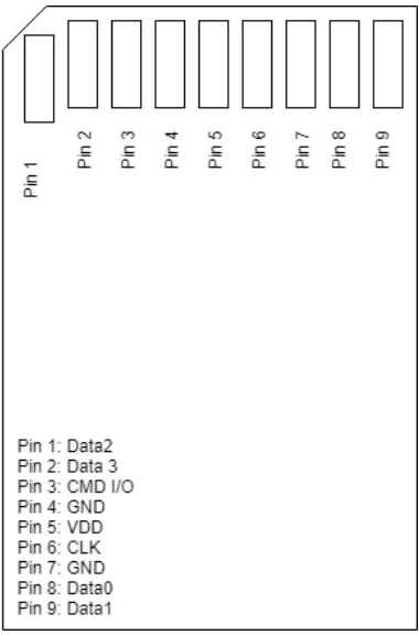
[image:25.612.219.409.134.422.2]Pinout
Figure 3.1: SD Card Pinout
Bus protocol
The default mode is standard SD mode, but is can be changed to support a slow SPI mode. This
protocol selection is performed with the first reset command after power up. By default, the card
starts in SD mode. To change it to SPI mode, a CS signal is asserted when the SD Card Controller
asserts a reset command. This protocol selection once done, cannot be undone or changed until
the next power cycle.
In SPI mode, card only uses 1 bit data bus. All the commands are in multiple of 1 byte. New
3.4 SD Card Protocols 14
3.4
SD Card Protocols
3.4.1
Initializing the card
While initializing the card, the card is most probably in the idle state. Hence, only legal
com-mands are CMD0, CMD1, ACMD41, CMD58 and CMD59. Any other command asserted will
set R1[2] bit.
Initialization of SD and MMC card have some primary difference in the command sequence.
The steps are mentioned below:
1. SPI clock is set to 400 kHz. This is essential for compatibility between SD card types.
(SDSC and MMC in this case).
2. SD Card Controller instructs the SD card to communicate using SPI by setting SS and CS
lines. Then, the SDCLK is toggled for 74 clock pulses before sending any command word.
This step is necessary for the card to initialize all the internal registers.
3. CMD0 is asserted to reset the card. Bit sequence: 01 000000 00000000 00000000 00000000
00000000 1001010 1
4. CRC check is ignored in SPI mode. But, the card is expecting a CRC check after reset.
Hence, a default value of 0x95 is sent with CMD0. To make this simple, this CRC byte is
sent with every command.
5. The SD card responds with the message (00000001) which indicates that the card is now
in Idle state. This message is received by holding CS line low and MOSI line high.
6. CMD58 is asserted to check the operating conditions register (OCR) of the SD card. This
register contains information like voltage, version number, special functions, etc. This
3.4 SD Card Protocols 15
2.7v to 3.6v). The SD card responds with a 40-bit word (say R2) where the first 8 bits are
standard SD card response while the next 32 bits contain information specific to that SD
card. R2[39:32] – If successful, the value will either be 00000001 or 00000101 depending
on the SD card. R2[31:28] – Version number R2[27:12] – Reserved for additional/special
functionality R2[11:8] – Voltage code R3[7:0] – CRC The response to this command tells
if the SD card is compatible with this controller.
7. CMD55 and ACMD41 are asserted to initialize the SD card internally.
8. Step 7 may have to be repeated several times depending on the type of the card. The steps
mentioned above also vary from card to card, and additional steps or more iterations of the
above steps are needed to successfully initiate a card. SD Card initialization routine
3.4.2
Data Transfer
In data transfer transactions, a data block is received or sent after the command response. This
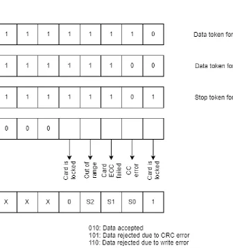
data block is transferred in the form of a data packet which consists of Token, Data Block and
3.4 SD Card Protocols 16
Figure 3.2: SD Card Data Packet
There are three data tokens depending on the CMD asserted. If a valid response cannot be
sent by the SD card, an error packet is sent; described as the fourth byte in Fig. 2.2 is the
3.4 SD Card Protocols 17
3.4.2.1 Writing a block of data to SD card
Once the card is initialized, data transfer operations are pretty straight forward. For writing a
block of data:
1. CMD24 is asserted. Once, a valid response (11111110) is obtained, the host controller
sends a data packet to the card.
2. The card sends a data response as soon as it received the data packet from the host
con-troller. This response consists of a busy flag. The host controller must wait until the busy
flag is cleared to perform a new transaction[29].
3.4.2.2 Reading a block of data from SD card
For reading a block of data:
1. CMD17 is asserted. Once, a valid response (11111110) is sent to the host controller and
the card begins the read operation. The host controller then receives the block of data from
the SD card.
2. Once the valid token is detected, the host controller obtains the data field and CRC bytes.
The CRC bytes must be transmitted to the controller even though CRC information is not
necessary.
Chapter 4
Device Under Test
This chapter discuses in detail the DUT Architecture, Design modifications and Communication
protocols.
The SD Card Controller IP operates as an SPI Master module. It supports SPI bus accesses
and communication with SD/MMC Cards.
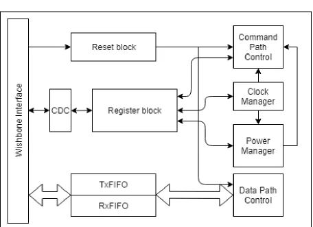
This module communicates with the master controller using wishbone interface. The
inter-face is responsible for creating clocks and reset signals for the module. Register block
con-tains all the registers that are to be written to or read from to successfully carry out a task like
block_read() or block_write(). The values and the order in which those values are written to the
register file is described in the SD protocol. Clock manager creates SPI clock. Power manager
19
4.1 IO Ports 20
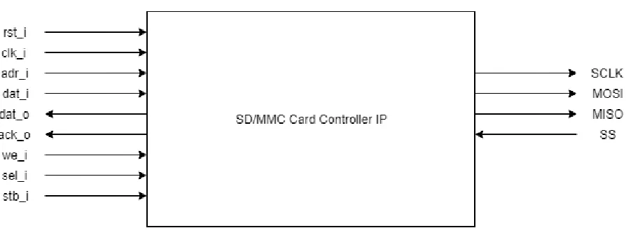
[image:32.612.84.531.133.301.2]4.1
IO Ports
Figure 4.2: SD/MMC Controller IO ports
This DUT has a standard wishbone interface to communicate with the master controller
(proces-sor/mcu) and an SPI interface to communicate with the SD/MMC card.
4.2
Register File
The register description for each register is given below. A typical SD Card controller DUT
consists of all these registers. A few registers are added to this controller especially to relieve
the complicated SD card protocols. For eg. Initializing an SD card consists of 10-12 command
assertions. This DUT enables the user to do the same operation using less than 3 steps. The
4.2 Register File 21
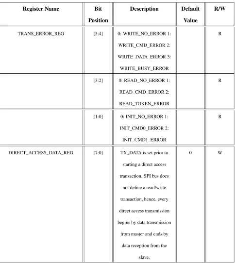
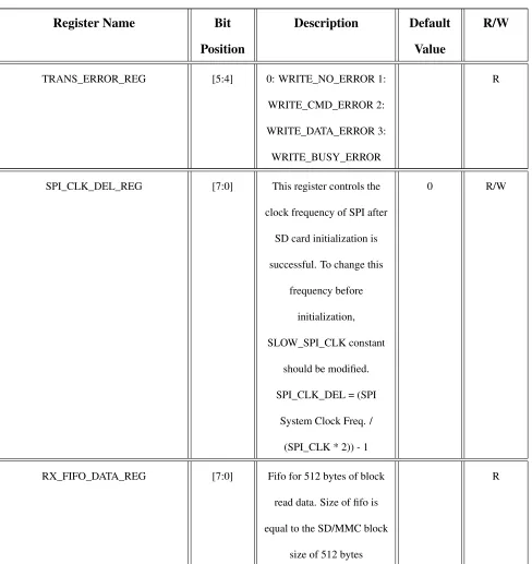
Table 4.1: SD/MMC Controller Registers
Register Name Bit Position
Description Default Value
R/W
TRANS_ERROR_REG [5:4] 0: WRITE_NO_ERROR 1:
WRITE_CMD_ERROR 2:
WRITE_DATA_ERROR 3:
WRITE_BUSY_ERROR
R
[3:2] 0: READ_NO_ERROR 1:
READ_CMD_ERROR 2:
READ_TOKEN_ERROR
R
[1:0] 0: INIT_NO_ERROR 1:
INIT_CMD0_ERROR 2:
INIT_CMD1_ERROR
R
DIRECT_ACCESS_DATA_REG [7:0] TX_DATA is set prior to
starting a direct access
transaction. SPI bus does
not define a read/write
transaction, hence, every
direct access transmission
begins by data transmission
from master and ends by
data reception from the
slave.
4.2 Register File 22
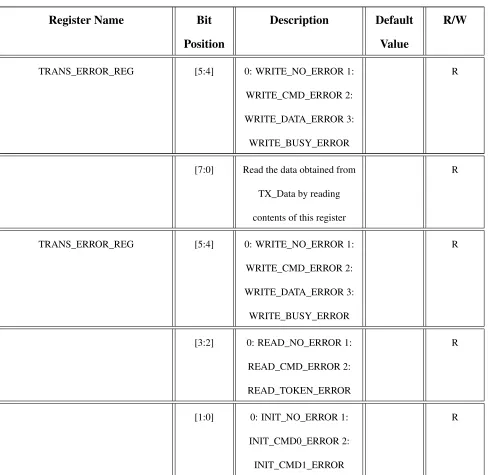
Table 4.1: SD/MMC Controller Registers
Register Name Bit Position
Description Default Value
R/W
TRANS_ERROR_REG [5:4] 0: WRITE_NO_ERROR 1:
WRITE_CMD_ERROR 2:
WRITE_DATA_ERROR 3:
WRITE_BUSY_ERROR
R
[7:0] Read the data obtained from
TX_Data by reading
contents of this register
R
TRANS_ERROR_REG [5:4] 0: WRITE_NO_ERROR 1:
WRITE_CMD_ERROR 2:
WRITE_DATA_ERROR 3:
WRITE_BUSY_ERROR
R
[3:2] 0: READ_NO_ERROR 1:
READ_CMD_ERROR 2:
READ_TOKEN_ERROR
R
[1:0] 0: INIT_NO_ERROR 1:
INIT_CMD0_ERROR 2:
INIT_CMD1_ERROR
4.2 Register File 23
Table 4.1: SD/MMC Controller Registers
Register Name Bit Position
Description Default Value
R/W
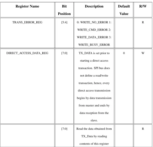
TRANS_ERROR_REG [5:4] 0: WRITE_NO_ERROR 1:
WRITE_CMD_ERROR 2:
WRITE_DATA_ERROR 3:
WRITE_BUSY_ERROR
R
DIRECT_ACCESS_DATA_REG [7:0] TX_DATA is set prior to
starting a direct access
transaction. SPI bus does
not define a read/write
transaction, hence, every
direct access transmission
begins by data transmission
from master and ends by
data reception from the
slave.
0 W
[7:0] Read the data obtained from
TX_Data by reading
contents of this register
4.2 Register File 24
Table 4.1: SD/MMC Controller Registers
Register Name Bit Position
Description Default Value
R/W
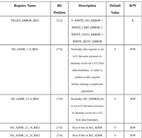
TRANS_ERROR_REG [5:4] 0: WRITE_NO_ERROR 1:
WRITE_CMD_ERROR 2:
WRITE_DATA_ERROR 3:
WRITE_BUSY_ERROR
R
SD_ADDR_7_0_REG [7:0] Normally, this register is set
to 0, because accesses to
memory occur on a 512 byte
data boundary. A value is
written to this register
before starting a read/write
operations
0 R/W
SD_ADDR_15_8_REG [7:0] Normally, SD_ADDR[8] bit
is set to 0, because accesses
to memory occur on a 512
byte data boundary.
0 R/W
SD_ADDR_23_16_REG [7:0] Next 8 bits of SD_ADDR 0 R/W
4.2 Register File 25
Table 4.1: SD/MMC Controller Registers
Register Name Bit Position
Description Default Value
R/W
TRANS_ERROR_REG [5:4] 0: WRITE_NO_ERROR 1:
WRITE_CMD_ERROR 2:
WRITE_DATA_ERROR 3:
WRITE_BUSY_ERROR
R
SPI_CLK_DEL_REG [7:0] This register controls the
clock frequency of SPI after
SD card initialization is
successful. To change this
frequency before
initialization,
SLOW_SPI_CLK constant
should be modified.
SPI_CLK_DEL = (SPI
System Clock Freq. /
(SPI_CLK * 2)) - 1
0 R/W
RX_FIFO_DATA_REG [7:0] Fifo for 512 bytes of block
read data. Size of fifo is
equal to the SD/MMC block
size of 512 bytes
4.2 Register File 26
Table 4.1: SD/MMC Controller Registers
Register Name Bit Position
Description Default Value
R/W
TRANS_ERROR_REG [5:4] 0: WRITE_NO_ERROR 1:
WRITE_CMD_ERROR 2:
WRITE_DATA_ERROR 3:
WRITE_BUSY_ERROR
R
RX_FIFO_DATA_COUNT_MSB [7:0] MSB of
FIFO_DATA_COUNT. It
indicates the number of
entries currently in the FIFO
R
RX_FIFO_DATA_COUNT_LSB [7:0] LSB of
FIFO_DATA_COUNT. It
indicates the number of
entries currently in the FIFO
R
FIFO_FORCE_EMPTY 0 1: Forces FIFO EMPTY.
Deletes all the entries in the
FIFO. Self clearing
0 W
TX_FIFO_DATA_REG [7:0] Fifo for 512 bytes of block
write data. Size of fifo is
equal to the SD/MMC block
size of 512 bytes
4.3 Clocks 27
Table 4.1: SD/MMC Controller Registers
Register Name Bit Position
Description Default Value
R/W
TRANS_ERROR_REG [5:4] 0: WRITE_NO_ERROR 1:
WRITE_CMD_ERROR 2:
WRITE_DATA_ERROR 3:
WRITE_BUSY_ERROR
R
TX_FIFO_CONTROL_REG 0 1: Forces FIFO EMPTY.
Deletes all entries in FIFO.
Self clearing.
0 W
4.3
Clocks
This module has two clocks. One is the SPI System Clock (spiSysClk) and the other is Wishbone
Bus Clock (clk_i). Both these clocks have a duty cycle of 50%. Wishbone clock is bounded by
the value of spiSysClk. Max. frequency of clk_i is (spiSysClk * 5) while the minimum frequency
is equal to the frequency of spiSysClk.
4.4
Simplified Protocols for this DUT
The creator of this DUT has internalized all protocol transactions. The protocol is implemented
in the form of a request/action handshake. The type of transaction is determined by the value of
SPI_TRANS_TYPE_REG. The transaction can initialize the card, write a block of data to the
4.4 Simplified Protocols for this DUT 28
register is set. Once, SPI_TRANS_STS_REG is reset, error check is done by registering the
con-tents of SPI_TRANS_ERROR_REG. The transaction continues or ends depending on the type.
Thus, this level automation has simplified the complex SD protocol[30].
4.4.1
SD Card: Initialization
1. Set SPI_TRANS_TYPE_REG = SPI_INIT_SD
2. Set SPI_TRANS_CTRL_REG = SPI_TRANS_START
3. Wait for SPI_TRANS_STS_REG != TRANS_BUSY
4. Check for SPI_TRANS_ERROR_REG [1:0] == INIT_NO_ERROR
4.4.2
SD Card: Block data write
1. Write 512 bytes to SPI_TX_FIFO_DATA_REG
2. Set the SD block address registers: SD_ADDR_7_0_REG, SD_ADDR_15_8_REG, SD_ADDR_23_16_REG
and SD_ADDR_31_24_REG
3. Set SPI_TRANS_TYPE_REG = SPI_RW_READ_SD_BLOCK
4. Set SPI_TRANS_CTRL_REG = SPI_TRANS_START
5. Wait for SPI_TRANS_STS_REG != TRANS_BUSY
4.4 Simplified Protocols for this DUT 29
4.4.3
SD Card: Block data read
1. Set the SD block address registers: SD_ADDR_7_0_REG, SD_ADDR_15_8_REG, SD_ADDR_23_16_REG
and SD_ADDR_31_24_REG
2. Set SPI_TRANS_TYPE_REG = SPI_RW_READ_SD_BLOCK
3. Set SPI_TRANS_CTRL_REG = SPI_TRANS_START
4. Wait for SPI_TRANS_STS_REG != TRANS_BUSY
5. Check for SPI_TRANS_ERROR_REG[3:2] == READ_NO_ERROR
Chapter 5
Verification Methodology
A test environment is a collection of verification components that are designed to check if the
Device Under Test conforms to the design specifications. A typical test environment setup is as
follows:
1. Generate stimulus, sequences, transactions based on the DUT input BFM
2. Reset the DUT
3. Feed the generated sequences to the DUT.
4. Run the tests. Insert property checking/assertions.
5. Capture the outputs generated by the DUT
6. Compare them to the expected outputs
7. Verify if they are correct. Verify if the assertions fail.
8. Create a log file for errors/mismatches/failures
5.1 Layered Testbenches 31
All the above things can be done using a single file which merges all the components. But, as the
complexity of the DUT increases, verification effort increases exponentially. Hence, the concept
of layered test bench is used. Using a layered testbench (in SystemVerilog) involves creating
various classes that do a particular task and communicate with each other to achieve the final aim
of verifying the DUT.
Creating a layered test bench has various advantages. The testbench has a software like
construct which supports OOP. It is good for verification of complex, high level DUTs where a
lot of modules communicate with each other. In the test environment, each component (class)
can be individually edited/tweaked to make it more feature-rich. The testbench can be reused
to test a similar DUT by editing a few components to satisfy the requirements of that DUT.
This testbench can interact with modules written in C too enabling a more diverse, inclusive test
environment[19].
5.1
Layered Testbenches
5.1.1
Turning simulation into verification
Directed tests using Verilog to test the complete DUT is impractical as the level of abstraction
and the complexity of DUTs increases. Hence, a good verification methodology takes into
con-sideration the function DUT is supposed to perform. A test plan or verification plan is derived
based on this function as it is broken down property by property. This verification plan includes
methods to test each of these properties.
Complex systems should not be verified manually by looking at waveforms. This makes
the verification effort difficult and time consuming. Instead, automating the function checking
5.1 Layered Testbenches 32
described by the verification plan. To ease this process, a functionally correct model is created
to form the basis on which the DUT is compared against. Ideally, a verification process should
involve directed tests of low level modules to ensure 100% coverage, and then, as the level of
ab-straction increases, random stimulus should be inserted. Random test vectors test for bugs which
would have been otherwise undiscoverable, while directed tests give good overall coverage. As a
compromise between the two, constrained random tests are performed which helps achieve high
coverage by making use of a series of good engineering judgements[31].
5.1.2
3 C’s of verification
Coverage, checkers and constraints play a key role in the verification process. Checkers ensure
functional correctness. This is achieved by feeding random stimulus to a DUT to improving
coverage. Checkers can be implemented in SystemVerilog as assertions or using procedural
code. Recently, assertions are embedded inside the DUT and placed on external interfaces to
ease the verification effort.
Coverage also provides a measure of completeness of testing. It indicates that the goals set in
the test plan are met. When the simulation is done, SystemVerilog offers mechanism for coverage
collection. They could be property based coverage (cover directives) or sample based coverage
(covergroups).
Constraints help achieve test plan coverage goals by shaping the random vectors to ensure
the DUT is tested for corner cases. Without constraints, it’d be difficult to discover these corner
faults as the verification time will increase exponentially. Constraints ensure that corner cases
5.2 UVM 33
5.1.3
Engineering effort
Using constraints in random stimulus generation, verification effort shifts from writing directed
tests to designing automatic checkers and executable coverage models. This enables the random
stimulus to efficiently utilize resources to achieve higher coverage goals. This also makes the
verification process a little more predictable and transparent.
Using reusable environments saves engineering time. It allows flexibility to configure and use
various verification components. Hence, to ensure reusability and take advantage of automation,
a layered testbench architecture needs to be set. UVM architecture is thus designed, keeping in
mind all the above points.
5.2
UVM
UVM is a library of SystemVerilog constructs. It was created by Accelera based on OVM (Open
Verification Methodology v2.1.1). Its a method of verifying the functionality of digital hardware
using simulation. This hardware can be verified at behavioral, register transfer (RTL) or
trans-action level using Verilog, SystemVerilog, SystemC, VHDL, etc. based on the abstrtrans-action level
desired by the user [32]. UVM acts a bridge which facilitates simulation oriented methodologies,
hardware acceleration or emulation. It also supports assertion based verification[18].
Advantages of UVM [33]:
1. UVM Source Code is available.
2. Code reusability as a product, service or a framework.
3. Phasing extensions
5.3 UVM based test environment verification of SD/MMC Controller IP 34
5. TLM interfaces
6. Resource Database
7. End of Test Mechanism
8. Command line processor
5.3
UVM based test environment verification of SD/MMC
Con-troller IP
5.3.1
UVM classes
UVM library contains all the blocks that are needed for quick development of a reusable
verifi-cation environment in SystemVerilog.
Based on the usage and applications, UVM classes are divided into following categories:
Globals Classes included in this category contain a small list of data types, variables, func-tions and tasks that are scoped by uvm_pkg.
Base These classes consist of basic blocks that are needed to build any verification envi-ronment. They pass information between components and ports using interfaces. The core base
classes used in this testbench are described in the following sections. uvm_object, uvm_component,
uvm_transaction and uvm_root are core base classes that facilitate the modularity and reusability
of the test bench.
5.3 UVM based test environment verification of SD/MMC Controller IP 35
Factory The Factory is used to create UVM objects and components based on the config-uration provided by the user. Using this class type allows the user to configure the hierarchy
dynamically without breaking encapsulation.
Phasing All UVM classes are simulated in phases. The classes in this section describe the phasing capability provided by UVM.
Configuration and Resources They are a set of classes that provide configuration database. This database is used to store and load properties that are needed at configuration time as well as
run time.
Synchronization These classes are used for synchronization of processes.
Containers These classes contain parameterized data structures that provide queue and pool services.
Policies Each class in this type are used to perform a particular task like printing, compar-ing, recordcompar-ing, etc. for a uvm_object-based objects. They are not included in uvm_object to
enable user to print and compare without modifying the object class.
TLM This library provides an elaborate abstract transaction-level interfaces and ports that are used to transport data, which are generally whole transactions (objects) at one time. TLM
ports are inherently more reusable and modular.
Components This library forms the foundation of UVM. They encapsulate behavior or classes like drivers, scoreboards, etc. All the components are derived from this library directly
5.3 UVM based test environment verification of SD/MMC Controller IP 36
Sequencers Sequencers act like data arbiters that control transaction flow from multiple stimuluses.
Sequences Sequences encapsulate user defined methods that generate multiple sequence based transactions.
Macros Macros are used to improve productivity.
Register Layers These are abstract classes that are used to perform read/write operations to memory models inside the DUT.
Command Line Processor This library provides an interface to decode command line arguments.
5.3.2
Test plan
SD/MMC controller is verified like any other memory. Data is written to a location, and then
read back. If the data that is read matches the data that was written, the controller functions
properly [34].
The stimulus to the controller is 32 bit address and 8 bit data. Both of these stimuli are
randomized. The address is constrained to address only 2 MB (221locations) of memory, because
only that much memory is instantiated in the SD Model. This controller only reads and writes
data in multiples of a 512 byte block, an additional constraint that the start address of the data
block to be written or read is less than (221- 512 - 1). This ensures that the data block doesn’t go
out of bounds.
The operation of this DUT at a very abstract level can be divided into 4 tasks: write_to_controller_fifo,
5.3 UVM based test environment verification of SD/MMC Controller IP 37
to randomize these 4 tasks, so that they can read/write to any location in the SD card and at the
same time, the data inside the FIFO can be manipulated. But, due to absence of an interrupt
mechanism, synchronizing these tasks between the stimulus generator (sequencer in UVM) and
checker (monitor/scoreboard in UVM) would have been really difficult.
To avoid the above complications, a simpler test plan is created. The stimulus generator
generates random address and data values and feed it to the write_to_fifo_task. After receiving
an acknowledgement that the data has been successfully written to the TX_FIFO, a command
sequence directing the DUT to write the data stored in the FIFO to the SD card is sent. The
stimulus generator waits for a fixed amount of time and then, it polls for a TRANS_BUSY
flag. Once, the the busy flag is reset, the stimulus generator sends a command sequence to
the DUT to read the data block from the SD card back to the RX_FIFO in the DUT. The data
from the RX_FIFO is captured in the monitor by calling the task read_from_controller_fifo. To
synchronize the two events, a handshaking method is established between the stimulus generator
(driver) and the checker (monitor). Two events, run_monitor and run_driver are created. The
driver generator waits for run_driver to be triggered before it fetches the next write sequence
from the sequencer. At the same time, once the driver has successfully sent a read_from_sd_card
command sequence to the controller, run_monitor event is triggered, which tells the monitor to
start capturing the data from the controller’s RX_FIFO. The data written to the TX_FIFO by the
driver and the data captured from the RX_FIFO by the monitor are both compared in scoreboard
using TLM FIFOs. The scoreboard keeps a track of successful read and write transaction.
Functional coverage is obtained by creating coverpoints in the driver, where the random data
5.3 UVM based test environment verification of SD/MMC Controller IP 38
Figure 5.1: Testbench architecture
5.3.3
Testbench Architecture
Fig. 4.1 describes the testbench architecture implemented in this project. The following
subsec-tions describe each block in detail. Fig. 4.1 is a very broad overview of the architecture. Many
more blocks function inside these classes in shadows.
5.3.3.1 DUT
The DUT in this architecture refers to the SD/MMC controller IP from Opencores. This DUT is
modified to include an interrupt controller and a card detect which can be read via wishbone by
the master core.
5.3.3.2 Top module
This module connects the DUT and the verification environment components. It can be used to
5.3 UVM based test environment verification of SD/MMC Controller IP 39
5.3.3.3 Interface
Interface encapsulates connectivity and functionality. All the modules instantiated within the
environment can be connected using a single interface. This adds a level of abstraction and
granularity to connections between the modules. This enables addition and deletion of ports
throughout the system by just editing one interface.
5.3.3.4 Agent
Agent can be of two types: active or passive. Active agents contain all the three components
viz. driver, sequencer and monitor. A passive agent only contains the monitor; it samples DUT
signals, but doesn’t drive the DUT.
5.3.3.5 Sequencer, Driver and Monitor
A sequencer consists of transaction items that are declared using factory mechanism. These
transaction consists of a sequence of stimulus for the DUT to perform a protocol or a
func-tional operation like sd_init(), sd_block_write() and sd_block_read() in this test bench. These
sequences contain a series of tasks that are called. The driver drives the DUT using these tasks.
The sequencer sequences these tasks for the driver. Monitor samples the data from the DUT for
comparison in the scoreboard.
5.3.3.6 Coverage and Scoreboard
Scoreboard is a comparator which compares samples from the monitor against a database or table
or vectors to verify if the data processed by DUT is correct. Coverage offers coverpoints inside
5.3 UVM based test environment verification of SD/MMC Controller IP 40
5.3.3.7 Environment
Environment consists of static and dynamic components. DUT, interfaces, anything physical are
static components. Dynamic components are the components that are generated or modified at
run time. The environment encapsulates the agent, scoreboard, coverage collector, sequencers,
configuration databases, etc.
5.3.3.8 Test
Test defines the test scenario for the testbench. A UVM testbench is activated when run_test()
method is called. run_test() method is specified inside the initial block. A user can add testcases
by providing arguments to run_test().
5.3.3.9 Sequence item
This item consists of data fields required for stimulus generation.Stimulus is generated by
ran-domizing sequences. Data in sequence item is defined as rand data type. Constraints are also
added.
5.3.3.10 Sequence
Sequence generates series of sequence_items and sends it to driver using sequencer.
5.3.3.11 Wishbone BFM
Wishbone BFM acts as a Verilog module that generates stimulus signals for the SD/MMC
con-troller IP. Typically, this BFM is instantiated inside sd_mmc_tb_top module, but in this
5.3 UVM based test environment verification of SD/MMC Controller IP 41
5.3.3.12 SD card model
SD card model acts as the output device that connects to the SD/MMC controller. It is a
Chapter 6
Results and Discussion
This chapter presents the results of the test environment. The post-simulation tasks are listed
below:
• The DUT is verified using test sequences generated by the test environment and comparing
the outputs with the expected data. This data is available in the scoreboard in a 512 byte
packet.
The “SD/MMC Controller IP” was Synthesized on a different technology nodes using two
dif-ferent synthesis options, RTL logic synthesis and DFT Synthesis with a full scan methodology.
43
Figure 6.1: DUT Simulation
Table 6.1: Area, Power, Timing and DFT Coverage of AES Encryption
32nm 65nm 180nm
Area
Combinational Area(µm2) 145792.78 20903.4 145792.78
Buf/Inv Area(µm2) 6935.544 684.72 6935.544
Non-Combinational Area(µm2) 778261.15 103228.28 778261.15
Total Area(µm2) 924053.94 124231.68 924053.94
Power
Internal Power (W) 0.0200 6.268E-09 0.0200
Switching Power (W) 5.733E-04 1.755E-07 5.733E-04
Leakage Power (W) 3.981E-06 1.310E-07 3.981E-06
Total Power (W) 0.0206 3.128E-7 0.0206
Timing Slack (ns) 14.3880 17.4700 14.4070
DFT Coverage (%) 100 100 100
DUT Simulation, Wishbone Simulation, RX_FIFO, TX_FIFO, Console Window and the
[image:55.612.86.530.345.617.2]44
Figure 6.2: Wishbone Simulation
45
Figure 6.4: RX_FIFO Memory Map
46
Chapter 7
Conclusion
A verification IP is developed using UVM to verify a SD/MMC controller IP created by
Open-Cores.org. SystemVerilog with UVM classes is studied to create a completely reusable and
reconfigurable test environment. This environment thoroughly randomizes the data and address
to be written to the SD card. Protocol checking is done by asserting properties. This VIP enables
the user to have control on the stimulus generator and monitor to validate the operation of the
DUT and debug it incase it fails.
7.1
Future Work
The DUT and the verification environment presented in this paper has a tremendous scope for
improvement. Some of the ideas are presented below:
• An interrupt controller for the DUT can be developed to enable the micro-controller to
directly read the interrupt register using wishbone bus. This interrupt pin/register would
also make the verification job easier. This was one of the goals set before this projects and
7.1 Future Work 48
• The verification environment can be modified to not have hard time constraints to wait for
the read and write operations to be finished. Instead of having events across monitor and
driver - which is not an ideal - the interrupt pin can be polled.
• The four tasks read_from_fifo, write_to_fifo, read_from_sd_card and write_to_sd_card
can be randomized in the sequencer to have completely randomized test sequences for the
DUT. This would also reveal corner cases and the behavior of the DUT when it encounters
them.
• Functional Coverage can be improved by creating a wide range of stimulus vectors.
• SD card model can be improved to act as an SD as well as MMC card. So that the test
sequences can further be randomized. In this environment, the DUT sends both the
initial-ization procedures for SD and MMC card and the model responds the SD card procedure
which tells the DUT that the card detected was an SD card.
References
[1] T. Martin, The Insider’s Guide To The NXP LPC2300/2400 based Microcontrollers,
M. Beach, Ed. Hitex (UK) Ltd., 2007.
[2] V. S. Rashmi, G. Somayaji, and S. Bhamidipathi, “A Methodology To Reuse Random Ip
Stimuli In An Soc Functional Verification Environment,” in 2015 19th International
Sym-posium on VLSI Design and Test, June 2015, pp. 1–5.
[3] P. J. Ma, Y. Jiang, K. Li, and J. Y. Shi, “Functional Verification Of Network Processor,”
in 2011 International Conference on Electronics, Communications and Control (ICECC),
Sept 2011, pp. 1472–1475.
[4] P. Rashinkar, P. Paterson, and L. Singh, System-on-a-Chip Verification Methodology and
Techniques. Springer US, 2002.
[5] I. Kastelan and Z. Krajacevic, “Synthesizable SystemVerilog Assertions as a Methodology
for SoC,” in 2009 First IEEE Eastern European Conference on the Engineering of
Com-puter Based Systems, Sept 2009, pp. 120–127.
[6] S. A. Wadekar, “A RTL Level Verification Method For Soc Designs,” inIEEE International
References 50
[7] N. Gupta and C. Harakchand, “Embracing the FPGA Challenge for Processor Design
Ver-ification,” in2014 15th International Microprocessor Test and Verification Workshop, Dec
2014, pp. 39–43.
[8] K. Kayamuro, T. Sasaki, Y. Fukazawa, and T. Kondo, “A Rapid Verification Framework for
Developing Multi-core Processor,” in2016 Fourth International Symposium on Computing
and Networking (CANDAR), Nov 2016, pp. 388–394.
[9] K. Yasufuku, N. Oshiyama, T. Saito, Y. Miyamoto, Y. Nakamura, R. Terauchi, A. Kondo,
T. Aoyama, M. Takahashi, Y. Oowaki, and R. Bandai, “A Uhs-ii Sd Card Controller With
240mb/s Write Throughput And 260mb/s Read Throughput,” in 2014 IEEE Asian
Solid-State Circuits Conference (A-SSCC), Nov 2014, pp. 29–32.
[10] A. El-Yamany, “Echoing The "generality Concept" Through The Bus Functional Model
Architecture In Universal Verification Environments,” in2016 17th International Workshop
on Microprocessor and SOC Test and Verification (MTV), Dec 2016, pp. 77–80.
[11] Y. Yang, Y. Yang, L. Niu, H. Wang, and B. Liu, “Hardware System Design Of Sd Card
Reader And Image Processor On Fpga,” in 2011 IEEE International Conference on
Infor-mation and AutoInfor-mation, June 2011, pp. 577–580.
[12] Y. Yang, Y. Yang, T. Yu, and Y. Zheng, “Software Design Of Sd Card Reader And
Im-age Processor Based On Fpga,” in2011 International Conference on Mechatronic Science,
Electric Engineering and Computer (MEC), Aug 2011, pp. 1864–1867.
[13] R. Sethulekshmi, S. Jazir, R. A. Rahiman, R. Karthik, S. Abdulla M, and S. Sree Swathy,
“Verification Of A Risc Processor Ip Core Using Systemverilog,” in 2016 International
Conference on Wireless Communications, Signal Processing and Networking (WiSPNET),
References 51
[14] P. Zhou, T. Wang, X. Wang, and Y. Wang, “Hardware Implementation Of A Low Power Sd
Card Controller,” in2014 IEEE International Conference on Signal Processing,
Communi-cations and Computing (ICSPCC), Aug 2014, pp. 158–161.
[15] C. E. Cummings and T. Fitzpatrick, “OVM & UVM Techniques for
Termi-nating Tests,” 2011. [Online]. Available: http://www.sunburst-design.com/papers/
CummingsDVCon2011_UVM_TerminationTechniques.pdf
[16] Y. N. Yun, J. B. Kim, N. D. Kim, and B. Min, “Beyond UVM for practical SoC verification,”
in2011 International SoC Design Conference, Nov 2011, pp. 158–162.
[17] C. Spear and G. Tumbush,SystemVerilog for Verification, Third Edition: A Guide to
Learn-ing the Testbench Language Features. Springer Publishing Company, Incorporated, 2012.
[18] Universal Verification Methodology (UVM) 1.2 User’s Guide - Accellera.
[19] R. Salemi,The UVM Primer. Boston Light Press, October 29, 2013.
[20] S. Sarkar, G. S. Chanclar, and S. Shinde, “Effective IP reuse for high quality SOC design,”
inProceedings 2005 IEEE International SOC Conference, Sept 2005, pp. 217–224.
[21] D. Stow, I. Akgun, R. Barnes, P. Gu, and Y. Xie, “Cost Analysis And Cost-driven Ip Reuse
Methodology For Soc Design Based On 2.5d/3d Integration,” in2016 IEEE/ACM
Interna-tional Conference on Computer-Aided Design (ICCAD), Nov 2016, pp. 1–6.
[22] SD Host Controller Simplified Specification given by www.sdcard.org.
[23] C. S. Lin, K. Y. Chen, Y. H. Wang, and L. R. Dung, “A NAND Flash Memory Controller
for SD/MMC Flash Memory Card,” in2006 13th IEEE International Conference on
References 52
[24] A. El-Yamany, S. El-Ashry, and K. Salah, “Coverage Closure Efficient UVM Based Generic
Verification Architecture for Flash Memory Controllers,” in2016 17th International
Work-shop on Microprocessor and SOC Test and Verification (MTV), Dec 2016, pp. 30–34.
[25] G. Visalli, “UVM-based verification of ECC module for flash memories,” in2017 European
Conference on Circuit Theory and Design (ECCTD), Sept 2017, pp. 1–4.
[26] C. S. Lin, K. Y. Chen, Y. H. Wang, and L. R. Dung, “A NAND Flash Memory Controller
for SD/MMC Flash Memory Card,” in2006 13th IEEE International Conference on
Elec-tronics, Circuits and Systems, Dec 2006, pp. 1284–1287.
[27] O. Elkeelany and V. S. Todakar, “Data Archival To Sd Card Via Hardware Description
Language,”IEEE Embedded Systems Letters, vol. 3, no. 4, pp. 105–108, Dec 2011.
[28] ——, “Data Concentration And Archival To Sd Card Via Hardware Description Language,”
in2011 IEEE GLOBECOM Workshops (GC Wkshps), Dec 2011, pp. 625–630.
[29] S. Kim, C. Park, and S. Ha, “Architecture Exploration of NAND Flash-based Multimedia
Card,” in2008 Design, Automation and Test in Europe, March 2008, pp. 218–223.
[30] S. Fielding,spiMaster IP Core Specification, 2008.
[31] M. Courtnoy, “SoC Verification Growing Up Fast,” Breker Verification Systems, Tech.
Rep., 2013.
[32] K. Fathy and K. Salah, “An Efficient Scenario Based Testing Methodology Using UVM,”
in 2016 17th International Workshop on Microprocessor and SOC Test and Verification
References 53
[33] G. Sharma, L. Bhargava, and V. Kumar, “Automated Coverage Register Access Technology
on UVM Framework for Advanced Verification,” in 2018 IEEE International Symposium
on Circuits and Systems (ISCAS), May 2018, pp. 1–4.
[34] K. Khalifa, “Extendable generic base verification architecture for flash memory controllers
based on UVM,” in2017 IEEE 21st International Conference on Computer Supported
Appendix I
Source Code
I.1
Agent
1 c l a s s sd_mmc_agent e x t e n d s u v m _ a g e n t ;
2 ‘ u v m _ c o m p o n e n t _ u t i l s ( sd_mmc_agent )
3
4 u v m _ e v e n t run_mon ;
5 u v m _ e v e n t r u n _ d r v ;
6
7 s d _ m m c _ s e q u e n c e r s a _ s e q r ;
8 s d _ m m c _ d r i v e r s a _ d r v r ;
9 s d _ m m c _ m o n i t o r _ b e f o r e sa_mon ;
10
11
12 f u n c t i o n new ( s t r i n g name , uvm_component p a r e n t ) ;
I.1 Agent 55
14 e n d f u n c t i o n : new
15
16 f u n c t i o n v o i d b u i l d _ p h a s e ( uvm_phase p h a s e ) ;
17 s u p e r . b u i l d _ p h a s e ( p h a s e ) ;
18
19
20
21 s a _ s e q r = s d _ m m c _ s e q u e n c e r : : t y p e _ i d : : c r e a t e ( . name ( "
s a _ s e q r " ) , . p a r e n t ( t h i s ) ) ;
22 s a _ d r v r = s d _ m m c _ d r i v e r : : t y p e _ i d : : c r e a t e ( . name ( " s a _ d r v r " )
, . p a r e n t ( t h i s ) ) ;
23 sa_mon = s d _ m m c _ m o n i t o r _ b e f o r e : : t y p e _ i d : : c r e a t e ( . name ( "
sa_mon " ) , . p a r e n t ( t h i s ) ) ;
24 / / s a _ m o n _ a f t e r = s d _ m m c _ m o n i t o r _ a f t e r : : t y p e _ i d : : c r e a t e ( .
name ( " s a _ m o n _ a f t e r " ) , . p a r e n t ( t h i s ) ) ;
25 e n d f u n c t i o n : b u i l d _ p h a s e
26
27 f u n c t i o n v o i d c o n n e c t _ p h a s e ( uvm_phase p h a s e ) ;
28 s u p e r . c o n n e c t _ p h a s e ( p h a s e ) ;
29
30 s a _ d r v r . s e q _ i t e m _ p o r t . c o n n e c t ( s a _ s e q r . s e q _ i t e m _ e x p o r t ) ;
31 e n d f u n c t i o n
32
I.2 Config 56
I.2
Config
1 c l a s s s d _ m m c _ c o n f i g u r a t i o n e x t e n d s u v m _ o b j e c t ;
2 ‘ u v m _ o b j e c t _ u t i l s ( s d _ m m c _ c o n f i g u r a t i o n )
3
4 f u n c t i o n new ( s t r i n g name = " " ) ;
5 s u p e r . new ( name ) ;
6 e n d f u n c t i o n : new
I.3 Driver 57
I.3
Driver
1 c l a s s s d _ m m c _ d r i v e r e x t e n d s u v m _ d r i v e r # ( s d _ m m c _ t r a n s a c t i o n ) ;
2 ‘ u v m _ c o m p o n e n t _ u t i l s ( s d _ m m c _ d r i v e r )
3 f r a m e a ;
4 v i r t u a l s d _ m m c _ i f v i f ;
5 s d _ m m c _ t r a n s a c t i o n s d _ t x ;
6 u v m _ p u t _ p o r t # ( f r a m e ) p u t _ p o r t _ h ;
7 i n t e g e r i ;
8 i n t e g e r j ;
9 i n t e g e r k ;
10 r e g[ 3 1 : 0 ] a d d r ;
11 r e g[ 3 1 : 0 ] a d d r 1 ;
12 b i t d i r ;
13 l o g i c [ 7 : 0 ] r e s p B y t e ;
14 l o g i c [ 7 : 0 ] r x B y t e ;
15 l o g i c [ 1 : 0 ] smSt ;
16 r e g [ 7 : 0 ] c n t ;
17 / / i n t e g e r i ;
18 u v m _ e v e n t run_mon ;
19 u v m _ e v e n t r u n _ d r v ;
20 u v m _ e v e n t _ p o o l p1 ;
21
22 / / r e g s p i S y s C l k ;
I.3 Driver 58
24 f u n c t i o n new ( s t r i n g name , uvm_component p a r e n t ) ;
25 s u p e r . new ( name , p a r e n t ) ;
26 e n d f u n c t i o n: new
27
28 f u n c t i o n v o i d b u i l d _ p h a s e ( uvm_phase p h a s e ) ;
29 s u p e r . b u i l d _ p h a s e ( p h a s e ) ;
30 v o i d ’ ( u v m _ r e s o u r c e _ d b # ( v i r t u a l s d _ m m c _ i f ) : :
r e a d _ b y _ n a m e
31 ( . s c o p e ( " i f s " ) , . name ( " s d _ m m c _ i f " ) , . v a l ( v i f ) ) )
;
32
33 p1= u v m _ e v e n t _ p o o l : : g e t _ g l o b a l _ p o o l ( ) ;
34 r u n _ d r v =p1 . g e t ( " r u n _ d r v " ) ;
35 run_mon =p1 . g e t ( " run_mon " ) ;
36 p u t _ p o r t _ h = new ( " p u t _ p o r t _ h " , t h i s ) ;
37
38 e n d f u n c t i o n: b u i l d _ p h a s e
39
40 t a s k r u n _ p h a s e ( uvm_phase p h a s e ) ;
41 p h a s e . r a i s e _ o b j e c t i o n ( . o b j ( t h i s ) ) ;
42
43
44 b e g i n
45
I.3 Driver 59
47 @(p o s e d g e v i f . c l k _ i ) ;
48 v i f . r s t _ i = 1 ;
49 @(p o s e d g e v i f . c l k _ i ) ;
50 v i f . r s t _ i = 1 ;
51 @(p o s e d g e v i f . c l k _ i ) ;
52 v i f . r s t _ i = 1 ;
53 @(p o s e d g e v i f . c l k _ i ) ;
54 v i f . r s t _ i = 1 ;
55 @(p o s e d g e v i f . c l k _ i ) ;
56 v i f . r s t _ i = 1 ;
57 @(p o s e d g e v i f . c l k _ i ) ;
58 v i f . r s t _ i = 1 ;
59 @(p o s e d g e v i f . c l k _ i ) ;
60 v i f . r s t _ i = 1 ;
61 @(p o s e d g e v i f . c l k _ i ) ;
62 v i f . r s t _ i = 1 ;
63 @(p o s e d g e v i f . c l k _ i ) ;
64 v i f . r s t _ i = 0 ;
65
66
67 c o n f i g _ d u t ( v i f . d a t a _ o ) ;
68 $ d i s p l a y( " B e f o r e I n i t " ) ;
69
70
I.3 Driver 60
72
73
74
75 e m p t y _ f i f o ( ) ;
76
77 f o r e v e r b e g i n
78 s e q _ i t e m _ p o r t . g e t _ n e x t _ i t e m ( s d _ t x ) ;
79 a d d r 1 = s d _ t x . a d d r e s s ;
80 $ d i s p l a y ( " a d d r = %x " , s d _ t x . a d d r e s s ) ;
81 s e q _ i t e m _ p o r t . i t e m _ d o n e ( ) ;
82 w b _ b l o c k _ w r i t e ( s d _ t x . a d d r e s s ) ;
83 r d _ c m d _ f r o m _ s d ( v i f . d a t a _ o ) ;
84
85 p u t _ p o r t _ h . p u t ( a ) ;
86
87 end
88
89
90
91
92 $ w r i t e ( " T e s t s d o n e " ) ;
93 $ s t o p ;
94 end
95
I.3 Driver 61
97 e n d t a s k: r u n _ p h a s e
98
99
100
101 t a s k w b _ b l o c k _ w r i t e ( ) ;
102 i n p u t [ 3 1 : 0 ] a d d r e s s ;
103
104 b e g i n
105 i n i t ( v i f . d a t a _ o ) ;
106 e m p t y _ f i f o ( ) ;
107 s e t _ a d d r ( a d d r ) ;
108 f o r( i = 0 ; i < 5 1 2 ; i = i + 1 )
109 b e g i n
110 s e q _ i t e m _ p o r t . g e t _ n e x t _ i t e m ( s d _ t x ) ;
111 w _ t o _ f i f o ( s d _ t x . d a t a ) ;
112
113 a [ i ] = s d _ t x . d a t a ;
114 s e q _ i t e m _ p o r t . i t e m _ d o n e ( ) ;
115 end
116 w r _ c m d _ t o _ s d ( v i f . d a t a _ o ) ;
117 end
118 e n d t a s k : w b _ b l o c k _ w r i t e
119
120 t a s k w b _ b l o c k _ r e a d ( ) ;
I.3 Driver 62
122
123 b e g i n
124 i n i t ( v i f . d a t a _ o ) ;
125 s e t _ a d d r ( a d d r ) ;
126 f o r( i = 0 ; i < 5 1 2 ; i = i + 1 )
127 b e g i n
128 r _ f r o m _ f i f o ( ) ;
129 end
130 r d _ c m d _ f r o m _ s d ( v i f . d a t a _ o ) ;
131 run_mon . t r i g g e r ( ) ;
132 r u n _ d r v . w a i t _ t r i g g e r ( ) ;
133 end
134 e n d t a s k : w b _ b l o c k _ r e a d
135
136
137
138
139 t a s k w b _ r e a d ;
140 i n p u t d e l a y ;
141 i n t e g e r d e l a y ;
142
143 i n p
![Table 3.1: SD Card Command words [1]](https://thumb-us.123doks.com/thumbv2/123dok_us/67276.6347/22.612.78.552.160.664/table-sd-card-command-words.webp)