ABSTRACT
MOHAN, APARNA. Design and Verification of a DDR2 Memory Controller for System on Chip Education. (Under the direction of Dr. W. Rhett Davis.)
Design and Verification of a DDR2 Memory Controller for System on Chip Education
by Aparna Mohan
A thesis submitted to the Graduate Faculty of North Carolina State University
in partial fulfillment of the requirements for the Degree of
Master of Science
Computer Engineering
Raleigh, North Carolina 2014
APPROVED BY:
Dr. Paul D. Franzon Dr. Huiyang Zhou
DEDICATION
BIOGRAPHY
Aparna Mohan was born and brought up in Trivandrum, India, and spent much of her life there. In 2010, she graduated from College of Engineering, Trivandrum with a Bachelor of Technology degree in Applied Electronics and Instrumentation. Subsequently, she joined Indian Space Research Organisation in Bangalore, as a Scientist/Engineer. During her tenure at ISRO, she was involved in satellite sensor bench level testing, was responsible for digital design of the detector output processing algorithm in the Light Detection and Ranging Project, performed initial experiments and developed the data acquisition system for Lyman Alpha Photometer (a payload flown in India’s mission to Mars). Aparna’s two year tenure at ISRO gave her a chance to interact and work with the top researchers from the country. This experience helped her identify her interests and motivated her to enroll in a graduate program.
ACKNOWLEDGEMENTS
I would like to thank Dr. Rhett Davis for being my advisor over the last two semesters. My plan to graduate with a thesis would not have seen the light of day without his guidance and support. I would also like to thank him for funding me during the course of this project.
I learned the basics of Digital Design when I took the course taught by Dr. Paul Franzon. I believe that his classes kindled my interest in this domain. I would like to thank you professor, for the inspiration, the knowledge and for also serving on my thesis committee. I would also like to extend my gratitude to Dr. Huiyang Zhou for serving on my thesis committee.
TABLE OF CONTENTS
LIST OF TABLES . . . vii
LIST OF FIGURES. . . .viii
CHAPTER 1 INTRODUCTION . . . 1
1.1 Motivation . . . 1
1.2 Goal . . . 2
1.3 Thesis Outline . . . 2
CHAPTER 2 DDR2 AND AHB-LITE PROTOCOL OVERVIEW . . . 4
2.1 DRAM Architecture . . . 4
2.1.1 DRAM Commands . . . 6
2.1.2 Extended Mode Register Set(EMRS) . . . 7
2.1.3 Bank Activate . . . 7
2.1.4 Precharge All . . . 7
2.1.5 Refresh . . . 7
2.1.6 No Operation . . . 8
2.1.7 Read . . . 8
2.1.8 Write . . . 8
2.2 DDR2 State Diagram . . . 10
2.3 AHB-Lite Slave . . . 11
CHAPTER 3 REGISTER TRANSFER LEVEL IMPLEMENTATION . . . 12
3.1 DDR2 Controller:Top Level View . . . 12
3.2 Controller Modules . . . 13
3.2.1 Initialization Module . . . 13
3.2.2 Read/Write and Control Logic . . . 15
3.2.3 Command Generator . . . 17
3.2.4 Refresh Module . . . 19
3.2.5 Read Module . . . 20
3.2.6 Write Module . . . 21
3.2.7 Synchronous FIFO . . . 23
CHAPTER 4 VERIFICATION AND SYNTHESIS . . . 25
4.1 Introduction to Verification . . . 25
4.1.1 Why UVM ? . . . 26
4.2 UVM Testbench . . . 26
4.2.1 Sequencer . . . 26
4.2.2 Driver . . . 27
4.2.3 Monitor . . . 27
4.2.4 Agent . . . 27
4.2.5 Environment . . . 28
4.3 DDR2 QVIP . . . 29
4.3.1 Configuring DDR2 QVIP . . . 31
4.3.2 Sequencer . . . 32
4.3.3 Scoreboard and Assertions . . . 33
4.3.4 Debugging with QVIP . . . 33
4.3.5 ddr_DQS Preamble/Postamble Issue . . . 34
4.4 AHB-Lite QVIP . . . 36
4.5 Synthesis . . . 37
CHAPTER 5 CORTEX-M0 SYSTEM DESIGN . . . 38
5.1 System Overview . . . 38
5.1.1 Master Interface . . . 39
5.1.2 Slave Interface . . . 39
5.1.3 AHB-Lite Interconnect . . . 41
5.2 Verification and Debugging . . . 42
5.3 Results . . . 42
CHAPTER 6 CONCLUSION . . . 43
6.1 Future Scope . . . 44
BIBLIOGRAPHY . . . 45
APPENDIX . . . 47
Appendix A SEQUENCER FILES . . . 48
A.1 SEQUENCER FOR BL=4 . . . 48
LIST OF TABLES
Table 2.1 Description of Controller Interface Signals . . . 5
Table 2.2 DDR2 Frequently Used Commands . . . 6
Table 2.3 DDR2 important timing parameters . . . 9
Table 2.4 Description of AHB Slave Interface Signals . . . 11
Table 3.1 Initialization module interface . . . 14
Table 3.2 Read/Write module interface . . . 15
Table 3.3 Command Generator module interface . . . 17
Table 3.4 Refresh module interface . . . 19
Table 3.5 Read module interface . . . 20
Table 3.6 Write module interface . . . 21
Table 3.7 Synchronous FIFO interface . . . 23
LIST OF FIGURES
Figure 2.1 State Diagram of DDR2[Jes] . . . 10
Figure 3.1 Block Diagram of DDR2 Controller . . . 13
Figure 3.2 Command Generator . . . 18
Figure 3.3 Implementation of Refresh Module . . . 19
Figure 3.4 Read Module Waveforms with BL=4 . . . 20
Figure 3.5 Read Module Implementation . . . 21
Figure 3.6 Write Module Implementation[MP98]. . . 22
Figure 3.7 Write Module Waveforms . . . 23
Figure 3.8 Read Module Waveforms with BL=8 . . . 24
Figure 4.1 Constituents of Verification Component[Uvm] . . . 27
Figure 4.2 Top module of UVM testbench . . . 28
Figure 4.3 Structure of a test in UVM[Fit]. . . 29
Figure 4.4 QVIP and DUT interface . . . 30
Figure 4.5 Configuration of QVIP . . . 31
Figure 4.6 Transactions from QVIP . . . 32
Figure 4.7 Clock and Strobe Signals during Write . . . 35
Figure 4.8 AHB-Lite VIP Connections . . . 36
Figure 4.9 AHB-Lite VIP Configuration . . . 37
Figure 5.1 Configuration of the System On Chip . . . 39
CHAPTER
1
INTRODUCTION
1.1
Motivation
The semiconductor industry has seen far reaching breakthroughs in transistors per chip and perfor-mance in this decade. Advancements in VLSI make it possible to implement an entire system on a single die. A System-on-chip(SoC) is an integrated circuit that integrates all parts of an electronic system into a single chip. Because SoCs are generally associated with reduced system complexity and cost, and also relatively compact footprints, they are highly in demand[Fly11].
1.2. GOAL CHAPTER 1. INTRODUCTION
controller, a critical component of an SoC.
Traditionally, Synchronous Dynamic Random Access Memories(SDRAMs) were used in comput-ers. Advancements in memory architecture and performance owing to market demands led to a slew of better and faster memories. The invention of Dual Data Rate(DDR) SDRAMs was a boon to the computer industry. DDR2 SDRAM, its successor, represents another high speed memory available in the market. DDR2 SDRAMs have an internal data bus four times the width of the external data bus, which enables high speed operation. Most SoCs these days use DDR2 interfaces. In light of these advantages of the DDR2, we design a memory controller that can be interfaced to DDR2 memories.
It is a known fact that functional verification takes a lion’s share of the time and effort in the design cycle. Conventionally, System Verilog is used for verification in academic institutions. Universal Verification Methodology(UVM) is a standard gaining popularity in the industry for functional verification. UVM enables Verification Intellectual Property(VIP) , which are reusable components that are helpful to generate comprehensive testbenches. VIPs are used by SoC manufacturers as they save time spent developing testbenches and golden models. To explore the pros and cons of this emerging SoC verification technique, we make use of a standard DDR2 VIP for functional verification of the controller. We were provided a beta version of VIPs from Mentor Graphics- “Questa10.2c-beta" (QVIP) for this project.
Though the advantages of using UVM and verification IPs are undoubtedly many, it does come with its share of shortcomings. It takes a long time for a person without any prior background in verification to learn and understand UVM, VIPs, their libraries and structure. Introducing UVM and VIPs in the curriculum of verification courses can help students meet industry requirements.
1.2
Goal
The goal of this thesis is to provide a memory controller with an AHB-Lite slave interface and an AHB-Lite interconnect suitable for SoC education. UVM and VIPs have been incorporated in the verification process to study the impact of using standard libraries and reusable components in the design flow. The design is synthesized after ensuring that all design functionalities are implemented, and that there are no bugs. The controller is interfaced to a processor via an AHB-Lite interconnect and functionality of the SoC is to be verified by executing a simple program on the processor.
1.3
Thesis Outline
1.3. THESIS OUTLINE CHAPTER 1. INTRODUCTION
CHAPTER
2
DDR2 AND AHB-LITE PROTOCOL
OVERVIEW
This chapter summarizes the architecture of DDR2 memories and AHB-Lite systems. It starts with an introduction to dynamic memories in section 2.1. In section 2.2, access state machine of the DDR2 memory is described. Section 2.3 provides a brief description of the AHB-Lite protocol with an emphasis on AHB slaves.
2.1
DRAM Architecture
2.1. DRAM ARCHITECTURE CHAPTER 2. DDR2 AND AHB-LITE PROTOCOL OVERVIEW
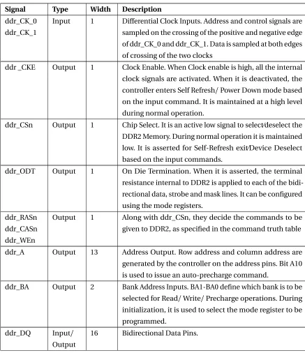
shows the functional description of the input and output pins of DDR2.
Table 2.1: Description of Controller Interface Signals Signal Type Width Description
ddr_CK_0 ddr_CK_1
Input 1 Differential Clock Inputs. Address and control signals are sampled on the crossing of the positive and negative edge of ddr_CK_0 and ddr_CK_1. Data is sampled at both edges of crossing of the two clocks
ddr _CKE Output 1 Clock Enable. When Clock enable is high, all the internal clock signals are activated. When it is deactivated, the controller enters Self Refresh/Power Down mode based on the input command. It is maintained at a high level during normal operation.
ddr_CSn Output 1 Chip Select. It is an active low signal to select⁄deselect the DDR2 Memory. During normal operation it is maintained low. It is asserted for Self-Refresh exit⁄Device Deselect based on the input commands.
ddr_ODT Output 1 On Die Termination. When it is asserted, the terminal resistance internal to DDR2 is applied to each of the bidi-rectional data, strobe and mask lines. It can be configured using the mode registers.
ddr_RASn ddr_CASn ddr_WEn
Output 1 Along with ddr_CSn, they decide the commands to be given to DDR2, as specified in the command truth table
ddr_A Output 13 Address Output. Row address and column address are generated by the controller on the address pins. Bit A10 is used to issue an auto-precharge command.
ddr_BA Output 2 Bank Address Inputs. BA1-BA0 define which bank is to be selected for Read/Write/Precharge operations. During initialization, it is used to select the mode register to be programmed.
ddr_DQ Input/ Output
2.1. DRAM ARCHITECTURE CHAPTER 2. DDR2 AND AHB-LITE PROTOCOL OVERVIEW
Table 2.1 Continued Signal Type Width Description
ddr_DQS Input/ Output
1 Data Strobe. It is generated by the memory during reads and by the controller during write operations. Data is generated at the positive and negative edge of the ddr_-DQS signal for read and is centered with respect to the ddr_DQS signal for writes. Data strobes are used in single-ended mode.
2.1.1 DRAM Commands
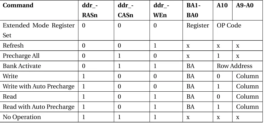
Memory Access is done by issuing commands to the DDR2. Table 2.2 details the frequently used DDR2 commands. Chip Select signal is asserted only if the device needs to be deselected and for power down mode of operation. Since power down mode is not commonly used, it is omitted from this section. Prior to normal operation, DDR2 SDRAM must be powered up and initialized as per the initialization sequence. This step is explained in chapter 3.
Table 2.2: DDR2 Frequently Used Commands
Command ddr_-RASn ddr_-CASn ddr_-WEn BA1-BA0 A10 A9-A0
Extended Mode Register Set
0 0 0 Register OP Code
Refresh 0 0 1 x x x
Precharge All 0 1 0 x 1 x
Bank Activate 0 1 1 BA Row Address
Write 1 0 0 BA 0 Column
Write with Auto Precharge 1 0 0 BA 1 Column
Read 1 0 1 BA 0 Column
Read with Auto Precharge 1 0 1 BA 1 Column
2.1. DRAM ARCHITECTURE CHAPTER 2. DDR2 AND AHB-LITE PROTOCOL OVERVIEW
2.1.2 Extended Mode Register Set(EMRS)
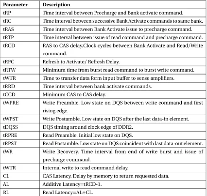
DDR2 has mode registers and extended mode registers that must be loaded with configuration values prior to normal operation. The EMRS command is used to initialize the mode registers. Bank address inputs are used to determine the register being programmed. The value to be programmed is issued to the address pins. Burst length, burst type, operating mode, additive latency, write recovery time, CAS Latency and DLL Reset/Enable are some of the variables that can be programmed using this command. EMRS requires tMRD to complete register write. Registers will retain the value unless programmed again. Table 2.3 shows the timing parameters.
2.1.3 Bank Activate
Bank Activate command or Row Address Strobe(RAS) must be issued before memory access can be executed. For this, ddr_CASn and ddr_WEn is held high and ddr_RASn goes low. Along with bank activate command, row address is given to the address pins and the required bank to be selected is given to the bank address pins. Data from the row is available at the output of the sense amplifier associated with the row after tRCD delay. It must be ensured that tRC has elapsed before issuing the next bank activate command[Tor11]. tRRD is the minimum time interval between activate commands to different banks.
2.1.4 Precharge All
Before another row in a bank can be accessed, the current bank must be deactivated and output of the sense amplifiers must be precharged to the necessary voltage. Precharge can be done for an individual bank or for all banks concurrently. It takes tRP, the precharge time, to complete precharg-ing. Once a bank is precharged, it is in the idle state. It must be activated before read/write can be issued to it. The Precharge All command precharges all the banks. Bank address bits become “don’t cares" during this operation. A10 bit is used to distinguish between the precharge and precharge-all commands.
2.1.5 Refresh
2.1. DRAM ARCHITECTURE CHAPTER 2. DDR2 AND AHB-LITE PROTOCOL OVERVIEW
Distributed Refresh:
Refresh cycle interval=Refresh time/number of rows (2.1)
Banks must always be in the idle state before issuing a refresh command. The Refresh command takes tREF to complete and banks will be in precharge state after refresh. During refresh, address bits are ignored[Mic03].
2.1.6 No Operation
No Operation(NOP) is issued by asserting all the command lines. It is used to insert wait states or delays when a command is being executed. NOP is important because it prevents DDR2 from transitioning to unwanted states when a command is being registered. The memory ignores values at address and data pins during NOP[Hyn].
2.1.7 Read
The Read command is used to read data from memory. It is issued after tRCD has elapsed from Bank Activate Command. Along with the read command, the column address from where the read is to be performed, and the bank address, are provided. Memory reads have an associated read latency(RL). RL=AL+CL. CL is the time taken for the data to appear at ddr_DQ pins from sense amplifier outputs. These values can be programmed with EMRS command. Output data appears in synchronization with strobe signal from the memory during data reads. It can be read at the rising and falling edge of ddr_DQS. ddr_DQS is driven low one clock cycle before ddr_DQ is issued. Both ddr_DQ and ddr_DQS go to high impedance upon completion of a burst.
Post read operation, the bank must be closed using a precharge command. Read with auto precharge(AP) allows precharge to be initiated automatically after a read. This is used to save cycles when dynamic DRAM accesses occur, as it eliminates the need to issue a separate precharge command. Bit A10 of the address pins is used to distinguish between normal read and read with AP. For read with AP, precharge is issued AL+BL/2 cycles after read with AP command. Table 2.3 describes other timings related to read command.
2.1.8 Write
2.1. DRAM ARCHITECTURE CHAPTER 2. DDR2 AND AHB-LITE PROTOCOL OVERVIEW
WL=RL-1. WL is the number of clock cycles from write command issue to rising edge of ddr_DQS. ddr_DQS is driven low half clock cycle before WL. Similar to read, write also has auto precharge op-tion that can be selected by a high level on A10. But precharge does not start till Write Recovery(WR) cycles after the end of data burst.
Table 2.3: DDR2 important timing parameters Parameter Description
tRP Time interval between Precharge and Bank activate command.
tRC Time interval between successive Bank Activate commands to same bank. tRAS Time interval between Bank Activate issue to precharge command. tRTP Time interval between issue of read command and precharge command. tRCD RAS to CAS delay.Clock cycles between Bank Activate and Read/Write
command.
tRFC Refresh to Activate/Refresh Delay.
tRTW Minimum time from burst read command to burst write command. tWTR Time to transfer data form input buffer to sense amplifiers.
tRRD Time interval between bank activate commands. tCCD Minimum CAS to CAS delay.
tWPRE Write Preamble. Low state on DQS between write command and first rising edge.
tWPST Write Postamble. Low state on DQS after the last data-in element. tDQSS DQS timing around clock edge of DDR2.
tRPRE Read Preamble. Initial low state on DQS.
tRPST Read Postamble. Low state on DQS coincident with last data-out element. tWR Write Recovery. Time interval from end of write burst and issue of
precharge command.
tWTR Internal write to read command delay.
CL CAS Latency. Delay by memory to return requested data. AL Additive Latency=tRCD-1.
2.2. DDR2 STATE DIAGRAM CHAPTER 2. DDR2 AND AHB-LITE PROTOCOL OVERVIEW
2.2
DDR2 State Diagram
Figure 2.1 shows the simplified state diagram of a DDR2 SDRAM.
2.3. AHB-LITE SLAVE CHAPTER 2. DDR2 AND AHB-LITE PROTOCOL OVERVIEW
2.3
AHB-Lite Slave
Advanced High Performance Bus(AHB) Lite protocol is a bus interface that supports a single master and enables high bandwidth operation[Ahb]. AHB slave interface signals are shown in table 2.4. The protocol operates in two phases: address and data. Address phase of any transfer occurs during the data phase of the previous transfer.
• When HREADY is high, master drives the address onto the bus after the rising edge ofHCLK. • In the next cycle, slave samples the address and commands generated in the previous cycle
and generatesHREADYOUT. Multiplexer generatesHREADY using thisHREADYOUT. • HREADY is sampled by the master on the third rising edge to determine if it must generate a
new transaction or wait for the previous transaction to complete.
Table 2.4: Description of AHB Slave Interface Signals Signal Type Width Description
HCLK Input 1 Bus clock. All signal timings are related to the positive edge of this clock.
HRESETn Input 1 Active low reset. HADDR Input 32 Address bus.
HBURST Input 3 Burst Type. The burst type indicates if the signal is a single transfer or part of a burst.
HSIZE Input 3 Transfer Size. This signal denotes if it is a byte, half-word or half-word in the bus.
HTRANS Input 2 Transfer Type. The transfer type indicates if it is a idle,non-sequential, sequential access or if the bus is busy.
HWDATA Input 32 Write data for data writes.
HWRITE Input 1 This signal goes high for write operation and is low for reads.
HREADY Input 1 Master initiates bus operation only when HREADY is high. Slave reads master signals when HREADY is high.
HRDATA Output 32 Read data for data reads.
CHAPTER
3
REGISTER TRANSFER LEVEL
IMPLEMENTATION
3.1
DDR2 Controller:Top Level View
A memory controller translates requests from requester into DDR2-understandable commands. The controller acts as the main logic that connects processors, high speed input-output devices and the memory system to each other[Ake10]. The primary function of the controller is to manage the flow of data between the processor, input-output devices and the memory system, correctly and efficiently. The controller described in this document is designed to work with a 256Mb(16Megx16) DDR2 SDRAM operating at 400MHz. It supports burst-4 and burst-8 operations, and accesses to all four banks of DDR2. It has two interfaces- an AHB slave interface through which it communicates with the bus master(front-end) and a DDR2 side interface(back-end). First-in-first-out(FIFO) registers are used at the AHB and DDR2 interfaces to enable communication with systems operating at different data rates. Figure 3.1 shows the block diagram of the controller. All the blocks are implemented in Verilog.
The main functions of the controller are:
3.2. CONTROLLER MODULES CHAPTER 3. REGISTER TRANSFER LEVEL IMPLEMENTATION
Figure 3.1: Block Diagram of DDR2 Controller
• Provide commands(data read/write) and signals(strobes) for DDR2 access. • Memory Mapping.
• Periodic refresh of memory.
• Data conversion from dual rate to AHB supported rates.
3.2
Controller Modules
The following sections discusses the functionality and implementation of various sub-modules in the controller.
3.2.1 Initialization Module
3.2. CONTROLLER MODULES CHAPTER 3. REGISTER TRANSFER LEVEL IMPLEMENTATION
Table 3.1: Initialization module interface Port Name Direction Width Description
ddr_CK_0 input 1 Top level clock input.
reset input 1 Global reset.
start_init input 1 Initialization starts when this signal goes high.
finish_init output 1 Finish initialization signal is asserted at the end of initialization.
RASn_init, CASn_init, WEn_init, CSn_init, CKE_init, ODT_init
output 1 Command signals to DDR2 during initializa-tion.
BA_init output 2 Mode register selectors during initialization. A_init output 13 Opcode to be written into mode registers initialize_reg output 1 Asserted during initialization and goes low
at the end of initialization.
The various steps in initialization are outlined below: 1. Start clock and maintain stable condition.
2. Apply NOP and takeCKE_inithigh.
3. Wait minimum of 400ns and then issue precharge all command. NOP or deselect is applied during the 400ns period. After issuing precharge command, wait for tRP=4 cycles for precharge phase to complete.
4. Issue Extended Mode Register Set (EMRS) command to EMR(2). Wait for tMRD=2 cycles before issuing any other command.
5. Issue EMRS command to EMR(3).
6. Issue EMRS command to EMR(1) to enable DLL. Set Additive Latency if needed to enable posted CAS operation.
7. Then issue Mode Register Set(MRS) to MR for DLL Reset.
8. After this, precharge all (lasting for 4 cycles) and 2 auto-refresh commands are applied (tRC=15).
9. Program the operating parameters in MR without resetting the DLL. Here the CAS Latency (CL=4), Write Recovery(WR=2) and Burst Lengths(BL=4) are set.
3.2. CONTROLLER MODULES CHAPTER 3. REGISTER TRANSFER LEVEL IMPLEMENTATION
Whenstart_initis asserted, a Finite State Machine(FSM) is used to traverse across all the aforemen-tioned steps. The delays associated with commands such as tMR,tPRE,tRFC are modeled using counters.
3.2.2 Read/Write and Control Logic
The main functions of this module are summarized below:
• Read and write control machines are implemented. • Generate enables for all the interface FIFOs.
• Generate control signals for all other modules.
An AHB-Lite slave as described in chapter 2 is used as the slave port of the controller. The AHB-Lite slave protocol is implemented using state machines in this module. Read and Write are the only operations issued by the AHB-Lite master. The controller handles all other operations required by the DRAMs. To do a read, theHWRITEsignal is forced low whenHSEL_Controller, HTRANS[1] and HREADY is high, which triggers the control machine that does the read. The data read from the memory is stored in two separate half-word FIFOs. The FIFO may be read whenever it is nonempty. To do a write, theHWRITEsignal is asserted with the same conditions mentioned for read. A separate control machine handles writes. The basic flow of the control machine implemented in this module is depicted in Figure 2.1.
Table 3.2: Read/Write module interface Port Name Direction Width Description
ddr_CK_0 input 1 Clock input.
rst input 1 Active low reset.
HSEL_Controller input 1 Slave select from AHB-Lite decoder. normal_op output 1 Asserted when normal mode is enabed.
HADDR input 1 32 bit AHB input address.
HTRANS input 2 AHB Transfer type: Idle, Non-sequential or Sequential.
HBURST input 3 Burst type of AHB:Single or INCR4 Burst.
HREADY input 1 Ready status of slaves.
HWRITE input 1 AHB read/write command.
3.2. CONTROLLER MODULES CHAPTER 3. REGISTER TRANSFER LEVEL IMPLEMENTATION
Table 3.2: Continued Port Name Direction Width Description
RAS_cm,CAS_cm, WE_cm
output 1 Commands generated during normal mode.
BA_cm output 2 Bank select output.
A_cm output 13 Row and column address select.
data_reg1,z_reg1 output 1 Data enable and DQS mask for write mod-ule.
read_en_reg output 1 Read enable for read module. write_to_fifo1,
read_from_fifo1
output 1 Data FIFO1 control signals.
write_to_fifo2, read_from_fifo2
output 1 Data FIFO2 control signals.
fifo_rst_reg1, fifo_rst_reg2
output 1 Reset signals for FIFOs.
ahb1 output 1 AHB FIFO read enable.
wr_en_ahb,rst_ahb, rd_en_ahb
output 1 Control signals for AHB FIFO.
3.2.2.1 Timing Limits
The controller is responsible for issuing operations to the DRAM and ensuring that the timing requirements of the DRAMs are met. DDR2 DRAMs have a number of timing limitations that are set by their specification and by the value stored in Mode Registers. Table 2.3 summarizes the various limits. The timing parameters are based on the JESD79-2F DRAM, which comes in a number of speed grades. The table shows the number of clocks for each parameter at 400 MHz. tRRD and tCCD are automatically met in this design as AHB-Lite master issues the next command after the previous command has completed execution. The mode registers are programmed to setAL=3, CL=4, BL=4, WR=2. Read/write operations enable the auto-precharge feature of DDR2.
A global counter is used to store the latency associated with an instruction. The counter value depends on:
• Type of instruction - whether it is a read/write.
• The time interval between successive bank activate commands, tRC.
3.2. CONTROLLER MODULES CHAPTER 3. REGISTER TRANSFER LEVEL IMPLEMENTATION
• Write Recovery time, tWR. • Burst Length.
3.2.2.2 Latency calculations
Read Latency(RL) is normally determined by AL and CL. Since auto-precharging is enabled, precharge related timings must also be considered. Internal precharge issue time is determined by the maxi-mum of tRTP cycles and BL/2 cycles. For BL=4, both values are equal to two and for BL=8, tRTP=4.
RL=AL+CL+RTP+RP. Write latency(WL) can be calculated similarly, with the addition of write recov-ery time to the calculations, givingWL=AL+CL-1+BL/2+WR+RP. Before issuing the next command to DDR2, it must be ensured that tRC is satisfied. To account for tRC, the global counter value for reads and writes depends on the maximum of RL, WL and tRC.
3.2.3 Command Generator
DDR2 memory goes through three main stages of operation: Initialization, normal mode for read/ write and refresh mode. The commands generated in the different modes must be combined properly before being issued to the back-end memory. The memory can enter undefined states of operation if signals from all the modules are not synchronized carefully. Commands generated must be issued to the memory at the negative clock edge, which will then be read by the memory during the subse-quent positive clock edge.
Table 3.3: Command Generator module interface Port Name Direction Width Description
ddr_CK_0 input 1 Top level clock input.
reset input 1 Global reset.
initialize_reg input 1 Goes high when initialization is in progress. normal_op input 1 Goes high when read/write logic is in
con-trol. RASn_init, CASn_init,
WEn_init, CSn_init, CKE_init, ODT_init
input 1 Commands from initialization module.
3.2. CONTROLLER MODULES CHAPTER 3. REGISTER TRANSFER LEVEL IMPLEMENTATION
Table 3.3: Continued Port Name Direction Width Description
A_init, A_cm input 13 Address bits from initialization and read/ write module.
RASn_cm, CASn_cm, WEn_cm
input 1 Commands from read/write module.
RASn_ref, CASn_ref, WEn_ref
input 1 Commands from refresh module.
ref_interrupt_reg input 1 Interrupt to indicate start of refresh opera-tion.
write_enable output 1 Write enable used by read and write module; generated based on current command. ddr_CKE, ddr_ODT,
ddr_CSn, ddr_CASn, ddr_RASn, ddr_WEn
output 1 Command Outputs to DDR2.
ddr_BA output 2 Bank address bits of DDR2. ddr_A output 13 Address bits output to DDR2.
As shown in figure 3.2, a multiplexer is used to select the output commands based on which module is currently active.
3.2. CONTROLLER MODULES CHAPTER 3. REGISTER TRANSFER LEVEL IMPLEMENTATION
3.2.4 Refresh Module
Table 3.4: Refresh module interface Port Name Direction Width Description
clk input 1 Top level clock input.
reset input 1 Global reset.
finish_init input 1 Indicates end of initialization and start of normal mode.
ready_status input 1 Controller status. If ready_status=1, con-troller is ready to accept a new command. Else, controller is busy executing the previ-ous command.
ref_interrupt_reg output 1 Refresh Interrupt that goes high to indicate refresh is in progress.
RASn_ref, CASn_ref, WEn_ref
output 1 Commands to DDR2 during refresh.
This module is responsible for generating refresh commands to the memory at the proper time. Burst refresh is implemented in this design. Refresh cycle interval count for burst refresh is obtained by dividing the refresh time(64ms) by the clock cycle time(5ns). A refresh counter is used in this module to count the number of clock cycles from the last refresh command in the normal mode.
Figure 3.3: Implementation of Refresh Module
3.2. CONTROLLER MODULES CHAPTER 3. REGISTER TRANSFER LEVEL IMPLEMENTATION
and worst case delay. The worst case delay for an instruction in the memory controller is calculated to be twenty five cycles. Before generating a refresh command, the module needs to know if the memory is idle or executing an instruction. The state of memory is reflected in ready_status signal. If the memory is idle, the refresh command is executed immediately. If not, the controller waits for HREADYOUT, which is same as ready_status, to go high and then issues refresh. An interrupt is raised by assertingref_interrupt_regsignal when refresh is in progress.
3.2.5 Read Module
The read module is used for data reads from the DDR2 memory. Data is referenced by the memory at the positive and negative edge of the strobe signal. Consequently, the strobe signal is used as reference to latch the data.read_en_regacts as the enable signal for this module. Two registers, one sensitive to the positive edge and the other sensitive to the negative edge of theDQSsignal are used to separate the dual edge triggered input data. The DQS referenced output is then passed through two registers sensitive to positive edge of the bus clock as shown in figure 3.5.
Table 3.5: Read module interface Port Name Direction Width Description
clk input 1 Top level clock input.
reset input 1 Global reset.
DQS input 1 Data strobe signal from memory.
DQ input 16 Data input from memory.
read_en_reg input 1 Enable signal to start read.
DQ_prev2 output 16 Ouput data at bus clock rate for FIFO2. DQ_prev1 output 16 Ouput data at bus clock rate for FIFO1.
3.2. CONTROLLER MODULES CHAPTER 3. REGISTER TRANSFER LEVEL IMPLEMENTATION
Before the module outputs are combined and transmitted on the data bus, they are written into two synchronous first-in-first-out(FIFO) registers. Control signals for FIFOs are generated by the read/write logic. Figure 3.4 shows the two clock synchronous outputs of read module.
Figure 3.5: Read Module Implementation
3.2.6 Write Module
Table 3.6: Write module interface Port Name Direction Width Description
clk input 1 Top level clock input.
reset input 1 Global reset.
data_reg input 1 Data enable that enables write to DDR2. z_reg input 1 Data mask for DQS preamble-postamble
correction.
3.2. CONTROLLER MODULES CHAPTER 3. REGISTER TRANSFER LEVEL IMPLEMENTATION
During write operations to a DDR2 SDRAM, the controller must provide the data strobe to the memory device center-aligned relative to the data. Data is transferred at both edges of strobe signal. Figure 3.6 shows a combinational logic using multiplexers to convert input data at single data rate to the double edge triggered form required by DDR2 protocol. However, synthesis cannot be performed on this circuit as it leads to combinational logic feedback loops. Custom design of the logic is required when placing the write module in the system.
Figure 3.6: Write Module Implementation[MP98]
3.2. CONTROLLER MODULES CHAPTER 3. REGISTER TRANSFER LEVEL IMPLEMENTATION
Figure 3.7: Write Module Waveforms
3.2.7 Synchronous FIFO
Synchronous FIFOs are used at the controller-DDR2 interface to store the data read from the mem-ory. Since data is generated at the positive and negative edges of the strobe signals, two instances of the FIFOs are used. One FIFO stores positive edge referenced data( Burst Sequence=0,2) and other FIFO stores data generated at the negative edge ( Burst Sequence=1,3). Storing data in two separate 16-bit FIFO registers help in faster data retrieval and combination. Figure 3.8 displays the FIFO read/write enable sequence for data reads for BL=8. Sequences 1 and 0 and sequences 3 and 2 must be concatenated from the respective FIFOs before being driven into the bus.Data converter moduleconcatenates data in the correct sequence. Synchronization between read enables to the FIFOs is ensured by the control logic.
Table 3.7: Synchronous FIFO interface Port Name Direction Width Description
clk input 1 Clock input.
rst input 1 Active high reset.
data_in input 16 Data input.
rd_en input 1 Read enable.
wr_en input 1 Write Enable.
data_out output 16 Data Output.
empty output 1 FIFO empty.
3.2. CONTROLLER MODULES CHAPTER 3. REGISTER TRANSFER LEVEL IMPLEMENTATION
CHAPTER
4
VERIFICATION AND SYNTHESIS
4.1
Introduction to Verification
Verification is extremely important for complex designs as it is necessary to detect and fix issues in the design at every stage. It must also be ensured that the design adheres to the specification[Spe06]. For the same purpose, verification is usually done alongside design, wherein independent tests which match the requirement are created. These tests are then run on the RTL design or design under test(DUT) to identify discrepancies at block and interface level. Testbenches are created to determine the correctness of DUT. The primary functions of a testbench are:
• Stimulus generation. • Apply stimulus to the DUT. • Store the response.
• Compare obtained behavior to expected behavior. • Measure progress against verification goal.
4.2. UVM TESTBENCH CHAPTER 4. VERIFICATION AND SYNTHESIS
Assertion Based Verification. This chapter describes the use of UVM for verification of the DDR2 controller and AHB-Lite slave from chapter 3.
4.1.1 Why UVM ?
UVM is a standardized methodology for integrated circuit verification, derived mainly from OVM. It was developed by the verification community for itself[Gla11]. It was developed by a group of industry experts and consultants, not a single electronic design automation(EDA) vendor. Accellera is responsible for standardizing UVM. The UVM library consists of component classes that can be used for building testbench components with Verilog/System Verilog/VHDL, and it runs on all major simulators. Reporting, stimulus generation and transactional level modeling for interfaces are some of the features supported by existing UVM classes.
Adding to the advantages of UVM, Mentor Graphics introduced Verification IPs(VIPs) with UVM architecture for standard interface verification. VIPs are reusable components which help in reducing the time spent writing verification components for specific DUTs. VIP components are integrated with the Questa debug environment and they make use of the viewing capabilities in Questa to provide transaction-level and signal-level debugging capabilities. Verification involves instantiating the VIP as a component in the testbench, connecting, and configuring the VIP. The built-in capabilities of VIP provide covergroups and testplans so that the metrics are in place to track whether all necessary scenarios are covered for that particular protocol. Section 4.3 describes how Questa Verification IP(QVIP) has been used for verifying the DDR2 controller. DDR2 QVIP is built using System Verilog for UVM environments[Jai]. It supports JEDEC’s JESD79-2F standard. AHB VIP is used to verify the AHB Lite slave interface. A brief introduction to UVM testbench and it’s components is provided in section 4.2 to aid in understanding QVIPs.
4.2
UVM Testbench
A UVM testbench consists of a reusable verification environment calledverification components. A verification component[Uvm]is a configurable verification environment that can be used for verification of DUTs, and has a fixed architecture that consists of elements performing different testbench functions. Figure 4.1 shows a typical verification component environment.
4.2.1 Sequencer
4.2. UVM TESTBENCH CHAPTER 4. VERIFICATION AND SYNTHESIS
Figure 4.1: Constituents of Verification Component[Uvm]
4.2.2 Driver
Driver is anactive entitythat converts data items produced by the sequencer into pin wiggles at the DUT inputs as defined in the specifications of the design interface.
4.2.3 Monitor
Monitor is apassive object that samples the signals from the DUT. It is used to detect protocol violations of the DUT, and gather coverage information.
4.2.4 Agent
4.2. UVM TESTBENCH CHAPTER 4. VERIFICATION AND SYNTHESIS
4.2.5 Environment
The environment(env) is the top level verification component.uvm_envis the environment class in UVM constructed to facilitate building of reusable verification components. Env can have more than one agent. The agent class is instantiated insideuvm_env. uvm_sequencer, uvm_driver and uvm_monitor are instantiated in uvm_agent. It also has configuration properties that are used to customize the agents as per the test requirements. The test to be run on the DUT has an instance of uvm_env and the test is instantiated in the top level module. DUT and the top module are the only module based components, the rest being class based components as shown in figure 4.2.
Figure 4.2: Top module of UVM testbench
4.2.6 Integrating the DUT
4.3. DDR2 QVIP CHAPTER 4. VERIFICATION AND SYNTHESIS
of a UVM testbench occurs in phases, with each one being responsible for executing a portion of the testbench. The build phase constructs verification components and connects them. In the connect phase, components and ports are connected. In the run-phase, the main body of the test is executed. Execution usually starts with therunphase, followed byconnect,runandreportphases.
Figure 4.3: Structure of a test in UVM[Fit]
4.3
DDR2 QVIP
4.3. DDR2 QVIP CHAPTER 4. VERIFICATION AND SYNTHESIS
is configured to match the requirements. The TLM model responds to the interface for various commands initiated by the controller. Figure 4.4 shows the DDR2 interface connecting wires. ddr_-DQSn, ddr_DM_TDQS_RDQS and ddr_TDQSn_RDQSn are not modeled in the controller, and hence, are not connected.
Figure 4.4: QVIP and DUT interface
ddr_if interface in the QVIP supports the following features from the DDR2 protocol described in chapter 2:
4.3. DDR2 QVIP CHAPTER 4. VERIFICATION AND SYNTHESIS
• Burst Lengths of 4 and 8.
• Scoreboard feature to ensure protocol correctness. • Preamble and Postamble timing detection.
• Refresh timings and inter-command latencies.
4.3.1 Configuring DDR2 QVIP
The controller designed in chapter 3 is suitable for interfacing with a 256 Mb DDR2. For this purpose, the QVIP was configured so that it matches the DUT parameters. Figure 4.5 shows the configuration parameters for this controller. Abstraction levels for controller, memory, clock and reset must be specified[Quea][Queb]. If the inputs for abstraction_level are (1,0), that end is configured as RTL, and if the inputs are (0,1), that end is TLM. The first argument is 1 for the controller, as RTL model is used. TLM memory model is used for DDR2, and hence the second argument is 1 for memory. Clock and reset has been generated in separate RTL modules. Further, the interface has been configured with the required number of banks, rows, columns and speed grade as shown.
4.3. DDR2 QVIP CHAPTER 4. VERIFICATION AND SYNTHESIS
4.3.2 Sequencer
The controller was first tested independently using inputs from a sequencer that generates a se-quence of read or write operations to random addresses. After that, it was tested with the AHB-Lite master sequencer. A ready signal is generated by the controller when it is ready to receive the next transaction, and this signal was used to decide when to provide the next input vector. Random constraints in System Verilog were used for the sequencer. Address and command were added as random variables of a class. The address being generated was constrained to a valid range, from 0 to 130968(2^22). Testing with this setup helped identify initial bugs. Typical transactions from QVIP are shown in figure 4.6. It must be noted that mvc_sequence class is not used for generating sequences and that QVIP comes with the transaction display feature.
4.3. DDR2 QVIP CHAPTER 4. VERIFICATION AND SYNTHESIS
After an initial testing without any AHB specific interfaces, the slave functionality was added. The sequencer was modified to generate AHB specific signals such asHTRANSand to respond toHREADY from slave. For BL=4 of DDR2, the sequencer described above with extra signals was used, and for BL=8, a different sequencer was used. Burst transfers requireHTRANSto generate a non-sequential transaction in the first cycle, followed by three sequential transactions, after which it settles at the idle state. If it is a write operation, the sequencer has to provide the write data in the first four cycles. This is achieved by adding global counters in the sequencer to keep track of current
HTRANSas shown in section A.2.
4.3.3 Scoreboard and Assertions
Scoreboard is used to compare the actual output with the expected output. QVIP has a scoreboard that can be used for checking data integrity from input to output. It is a TLM component and models the DDR2 memory in the form of a three dimensional array. It checks the data read and written, and reports errors if there is a mismatch between the write and reads from same location. Scoreboard feature of QVIP has been instantiated in the testbench and it helped identify the endiannness error that occurred due to wrong memory mapping.
Assertions are used to validate the behavior of a design. DDR2 QVIP assertions help in monitoring the bus and triggers an error message whenever a protocol violation is observed. These assertions were enabled in the testbench and helped identify issues in the design related to the order of instructions and timing.
4.3.4 Debugging with QVIP
This section discusses some of the important errors identified by enabling assertions in QVIP and how they were fixed.
Warning: (vsim-59300) MVC @ 87500 ps:
/top/ddr_if: Operating on a wire /top/ddr_if/ddr_RASn.ddr_RASn : Attempt
to convert hdl_bit (X) to a 2-state representation.
Fix: Reported after integrating all modules. This warning was reported in all the command signals, and caused the simulation to stop after a while. The reason was thatinitializefrom initialization module was causing "don’t cares" to get propagated in the command generator. The end signal of initialization and beginning of normal operation were properly synchronized to fix this.
Error: (vsim-60073) MVC @ 42282975 ps:
/top/ddr_if: DDR_MRS_EMRS_TMRD_NOT_MET:114 - <DDR_MRS_EMRS_TMRD_NOT_MET>
4.3. DDR2 QVIP CHAPTER 4. VERIFICATION AND SYNTHESIS
Warning: (vsim-51901) MVC @ 512975 ps for 512500 ps:
/top/ddr_if commands_stripe: Recognizing item
/top/ddr_if/commands_stripe:1, starting at 512975 ps, is not legal ddr
protocol at 512975 ps since change detected to wire
/top/ddr_if/ddr_WEn before hold time (512975 ps).
Fix: Commands were not getting registered at the DDR2 TLM model. This is because commands must be issued setup time before the clock edge. Command generation timing was changed accordingly.
Error: (vsim-60164) MVC @ 512975 ps: /top/ddr_if:
DDR_INIT_PRECH_ALL_NOT_FIRST_CMD_AFTER_NOP:199
-<DDR_INIT_PRECH_ALL_NOT_FIRST_CMD_AFTER_NOP> 1st command to be issued
after NOP should be Precharge-All."(See DDR2 JESD79-2F Protocol
Specification Section 3.3.1 )"
Fix: Initialization must begin with a Precharge-All command.
Error: (vsim-60057) MVC @ 527975 ps: /top/ddr_if ddr_transfer:
DDR_ILLEGAL_CAS_LATENCY:79 - <DDR_ILLEGAL_CAS_LATENCY> CAS latency
should be set according to interface and speed or user configured
values. "(See DDR2 JESD79-2F Protocol Specification Section 3.4.1 )"
Fix: CAS Latency and Additive Latency must be set to the same value.
Error: (vsim-60058) MVC @ 527975 ps: /top/ddr_if ddr_transfer:
DDR_ILLEGAL_WRITE_RECOVERY:80 - <DDR_ILLEGAL_WRITE_RECOVERY> Write
recovery values should be set according to interface type and speed or
according to user configured values."(See DDR2 JESD79-2F Protocol
Specification Section 3.4.1 )"
Fix: Write Recovery for AutoPrecharge was not programmed as per the speed grade. Error: (vsim-60090) MVC @ 2497975 ps: /top/ddr_if:
DDR_WR_WITH_AP_TO_CMD_TIMING_VIOLATION:140
-<DDR_WR_WITH_AP_TO_CMD_TIMING_VIOLATION> Any command after Write with
AP to same bank can be issued only after tWR+tRP is elapsed after the
burst completion."(See DDR2 JESD79-2F Protocol Specification Section
3.8.2 )"
Fix: For write operation with auto precharge, any other command can be issued only after tWR+tRP cycles after the burst completion, for both BL=4 and BL=8. The controller worked fine for BL=4, but time to complete BL=8 was not taken care of properly.
4.3.5 ddr_DQS Preamble/Postamble Issue
4.3. DDR2 QVIP CHAPTER 4. VERIFICATION AND SYNTHESIS
precise timing of strobe signal with respect to the DDR2 clock. Additionally,ddr_DQS, the strobe signal must be driven low before going to or coming from a tristate. The state whereddr_DQSis low just after a tristate( start of write) is called the preamble and the state whereddr_DQSis low just before it goes to tristate(end of write) is called the postamble. Timing values for preamble and postamble are defined in table 2.3. In this regard, QVIP reported the following error:
Error: (vsim-60189) MVC @ 169235000 ps: /top/ddr_if:
DDR_WR_POSTAMBLE_VIOLATION:238 - <DDR_WR_POSTAMBLE_VIOLATION> Write
postamble duration tWPST not met. "(See DDR2 JESD79-2F Protocol
Specification Section 3.6.4 )"
Error: (vsim-60199) MVC @ 169302510 ps: /top/ddr_if
preamble_to_postamble_dqs: DDR_DQS_NOT_VALID:243 - DDR_DQS_NOT_VALID
DQS bits cannot be invalid (X/Z)
Figure 4.7: Clock and Strobe Signals during Write
Reason:Timing violation of preamble and postamble parameters occur when precise timing is not maintained. Proper timing is usually obtained by using Delay Locked Loops in conjunction with on-chip delay elements[Cor04]. 90°ddr_DQSphase offset at the controller output can also solve this. But QVIP continued to give errors in spite of 90°offset. Figure 4.7 shows the signals at the controller output.
Apart from this issue, controller is working as per the requirements. No read/write discrepancies exist in the module. The performance summary of controller with DDR2 QVIP for BL=4 is shown below:
/top/ddr_if/transfer : Normal attempts = 8956 ,
successes = 4478 , efficiency = 50.00%
/top/ddr_if/write : Normal attempts = 1524 ,
successes = 1524 , efficiency = 100.00%
/top/ddr_if/read : Normal attempts = 2954 ,
successes = 2954 , efficiency = 100.00%
/top/ddr_if/initialize : Normal attempts = 1 ,
4.4. AHB-LITE QVIP CHAPTER 4. VERIFICATION AND SYNTHESIS
/top/ddr_if/activate_cmd : Normal attempts = 2954 ,
successes = 2954 , efficiency = 100.00%
/top/ddr_if/precharge_all : Normal attempts = 2 ,
successes = 2 , efficiency = 100.00%
/top/ddr_if/refresh : Normal attempts = 2 ,
successes = 2 , efficiency = 100.00%
/top/ddr_if/nop : Normal attempts = 57413 ,
successes = 57413 , efficiency = 100.00%
/top/ddr_if/MR_MR0 : Normal attempts = 2 ,
successes = 2 , efficiency = 100.00%
/top/ddr_if/EMR1_MR1 : Normal attempts = 3 ,
successes = 3 , efficiency = 100.00%
/top/ddr_if/EMR2_MR2 : Normal attempts = 1 ,
successes = 1 , efficiency = 100.00%
/top/ddr_if/EMR3_MR3 : Normal attempts = 1 ,
successes = 1 , efficiency = 100.00%
/top/ddr_if/ODT : Normal attempts = 7452 ,
successes = 7452 , efficiency = 100.00%
/top/ddr_if/commands_to_address : Normal attempts = 7444 ,
successes = 7443 , efficiency = 99.99%
---Summary : Normal attempts = 88709 ,
successes = 84230 , efficiency = 94.95%
======================================================================
4.4
AHB-Lite QVIP
Figure 4.8: AHB-Lite VIP Connections
4.5. SYNTHESIS CHAPTER 4. VERIFICATION AND SYNTHESIS
are provided to test the slave interface. Sequences match the processor requirements outlined in chapter 5. They are generated in a separate file and passed as arguments to the test . Example pro-grams provided with the VIPs are used with small configuration changes shown in figure 4.9[Cor13]. Test parameters need to be set in a separate file as shown:
parameter AHB_NUM_MASTERS = 1;
parameter AHB_NUM_MASTER_BITS = 1;
parameter AHB_NUM_SLAVES = 1;
parameter AHB_ADDRESS_WIDTH = 32;
parameter AHB_WDATA_WIDTH = 32;
parameter AHB_RDATA_WIDTH = 32;
Figure 4.9: AHB-Lite VIP Configuration
4.5
Synthesis
CHAPTER
5
CORTEX-M0 SYSTEM DESIGN
The Cortex-M0 processor is the smallest processor developed by ARM. It has a 32-bit Reduced Instruction Set Computing(RISC) processor core with ARMv6-M architecture intended mainly for micro-controller and embedded system applications[Yiu11]. This chapter discusses a SoC built around the Cortex-M0 processor and the DDR2 SDRAM controller developed in chapter 3. The synthesizable verilog netlist of the processor is obtained from the ARM DesignStart IP Portal. In the SoC under consideration, the processor(master) connects to the memory controller(slave) via a 32 bit AHB-Lite bus. The bus permits connection of two AHB-Lite slaves. Since a DDR2 memory model is not available, a 256Mb-dummy DDR2 memory is created. It has 16 bits of data organized in 13 rows, 7 columns and 4 banks. Here, the Cortex-M0 processor executes a program that prints the fibonacci series for a given number of iterations.
5.1
System Overview
5.1. SYSTEM OVERVIEW CHAPTER 5. CORTEX-M0 SYSTEM DESIGN
Figure 5.1: Configuration of the System On Chip
5.1.1 Master Interface
The Cortex-M0, being the bus master, generates the write data, address and control signals. 32-bit address and data transactions are generated on the bus. Table 5.1 describes the Master-Slave inter-faces. The Cortex-M0 does not generate locked transfers. Hence,HMASTLOCK is always 1’b0[Shi]. Though the protocol supports bursts of 4,8 and 16 beats, the processor does not produce burst transfers.HBURSTsignal from the processor is always 3’b000.HTRANSindicates the type of transfer: idle, busy, non-sequential or sequential. Only idle and non-sequential transfers are supported. The master uses an idle transfer(HTRANS=2’b00)when it does not want to perform a data transfer. Non-sequential transfer(HRANS=2’b10)indicates a single transfer, wherein the address and control signals are unrelated to the previous signals. Protection control signal,HPROT provide additional information about bus access such as if the transfer is an opcode fetch or data access. In this system,
HPROTsignal is ignored by the slave.
5.1.2 Slave Interface
The Memory Controller acts as a slave(Slave 1), and responds to the control signals and generates transactions as outlined in chapter 3. The controller runs at the system clock of 10 ns. It generates
0x40000000-5.1. SYSTEM OVERVIEW CHAPTER 5. CORTEX-M0 SYSTEM DESIGN
0x5FFFFFFF.
Table 5.1: Description of Mater-Slave Interface Signals Address and Control Data Transfer Response HADDR[31:0] HRDATA[31:0] HREADYOUT HWRITE HWDATA[31:0] HRESP
HSIZE[2:0] HREADY
HBURST[2:0] HPROT[3:0] HTRANS[1:0] HMASTLOCK
5.1.2.1 Dummy Memory
Since a memory is not available, a dummy memory is created for the purpose of simulation. An array of 64-bit registers that takes the formreg[63:0]ram[0:(2^size)-1]is used, where size refers to the total size of the DRAM in bytes after taking into consideration it’s dual data rate(size=22 for 256Mb). The commands and read/write addresses from the DDR2 controller to the memory are latched at the positive edge of the clock. Sample code for Bank Activate is shown below. Row and bank address is given along with the activate command. Column address is latched with the read/ write command.
if((ddr_CSn==1’b0)&&(ddr_RASn==1’b0)&&(ddr_CASn==1’b1)&&(ddr_WEn==1’b1))begin
row_add=ddr_A;
bank_add=ddr_BA;
read=1’b0;
write=1’b0;
end
5.1. SYSTEM OVERVIEW CHAPTER 5. CORTEX-M0 SYSTEM DESIGN
5.1.2.2 Memory Mapping
Cortex-M0 has a byte addressable space. Each address refers to 8 bits, and it generates 32 bits in a single transaction over the AHB-Lite bus. Addresses generated by the Cortex-M0 are hence multiples of 4. DDR2 memory stores 64 bits in one address, with the last 2 bits of the address to decide the start of output burst sequence. It supports Burst 4 by default. If the last two bits of the address are 01, sequences are generated in the order (1,2,3,0) and if they are 11, sequences will be (3,0,1,2). If A2,A1 and A0 represent the least significant three bits of the input address, (A2A1A0)=000 to 011 maps to burst sequences 0 and 1 of DDR2, and (A2A1A0)=100 to 111 maps to 2 and 3 of DDR2 bursts. Since we are interested in reading sequences starting at 0 or 2, we can neglect the last 2 bits from the controller address. A2 is used to select whether we require the upper or lower 32 bits.
While the Cortex-M0 only supports single burst transactions that are 32 bits long, DDR2 can read/write 64 bits in one transaction. The data mismatch can be solved in two ways: either read/ write 32 bits only to DDR2 in every transaction or for every write to DDR2, read 64 bits and write only 32 bits according to the input address. The first approach results in wasting memory capacity as essentially we are using only half the space by accessing 32 bits every-time. The second approach causes an increase in the number of cycles, but results in efficient use of memory space. In this system, the controller implements the read for every write approach.
5.1.3 AHB-Lite Interconnect
5.2. VERIFICATION AND DEBUGGING CHAPTER 5. CORTEX-M0 SYSTEM DESIGN
The AHB-Lite protocol is used with a data multiplexor and decoder[Ahb]. The master sends the ad-dress and control signals to all the slaves, with the decoder selecting the appropriate slave. Response data is send back to the master through the multiplexer as shown in figure 5.2.
5.2
Verification and Debugging
Both the DDR2 and AHB-Lite interfaces were verified independently using verification IP(VIP). Consequent to successful block level verification, these blocks were integrated with the processor. VIP provided does not assist to test a system that has two interfaces in parallel. It only supports execution of multiple tests in regression. To test the Cortex-M0 system, “waveform analysis and debug" was adopted. On integrating the system with the dummy memory and executing fibonacci.c program, it was observed that there were discrepancies in the memory read and writes. This hap-pened because of memory mapping inadequacies that were later taken care of. Another pitfall was the data-strobe synchronization modeling in the dummy memory vs the TLM model used to verify the controller. TLM model is designed after commercial DDR2 memories that have Delay Locked Loops(DLL) for aligning data and strobe signals for controller reads. Controller is designed to respond to these timings. Similar timings were missing in the dummy memory that were addressed by using additional clocks simulating aforementioned timings. It was observed that AHB command signals from the processor had glitches at the positive clock edges that were triggering the AHB slave state machine. To circumvent this, a negative edge sensitive flip-flop was used at the slave interface to distinguish between glitches at the positive edge, and true commands.
5.3
Results
CHAPTER
6
CONCLUSION
In this thesis, the design and verification of a DDR2 memory controller with an AHB-Lite slave port has been illustrated. Design verification is achieved using Universal Verification Methodology(UVM) and Questa Verification IP(QVIP) for the DDR2 and AHB Lite interfaces. This verification approach was adopted in the design flow to understand the potential advantages of using UVM testbenches over conventional System Verilog ones.
The UVM library uses classes as the primary components, with member functions to configure verification components according to the test requirements. Many standard functions are already implemented in the standard QVIP that is used. Predefined macros such as 'uvm_info and 'uvm_-error help in faster identification of the 'uvm_-error cause. System Verilog requires the user to write the logic for all the functions, and implement a golden reference model first before being able to use the model as a reference for verification.
6.1. FUTURE SCOPE CHAPTER 6. CONCLUSION
built in System Verilog, provides a foundation to quickly develop well-constructed reusable test environments. Fast construction of testbenches is required in system-on-chip(SoC) verification and this makes UVM based VIP an attractive option for verification.
However, there are a few problems with the above mentioned approach. First and foremost, it is difficult and time consuming for a person who has never used a verification language to learn verification methodology. Concepts like inheritance and virtual interfaces when combined with verification concepts such as checkers and monitors have a steep learning curve. On the other hand, this could be a motivation to introduce courses on UVM and VIPs as part of the curriculum to help students in get upto speed on industry expectations.
After using QVIPs for verification, a functional coverage of 94.95 % was obtained for the controller. Logic synthesis of the controller RTL yielded an area of 4542 um2. An SoC platform is developed with the DDR2 memory controller, a Cortex-M0 processor and a dummy memory using an AHB-Lite bus interconnect for the controller-processor interface.
6.1
Future Scope
• Extending the DDR2 controller to a Direct Memory Access(DMA) controller. A DMA controller allows subsystems within the SoC to access the system memory without processor intervention. If an SoC needs to be developed with multiple I/O devices requiring access to DDR2 memory, it is optimal to have a shared system bus containing the controller, processor and I/O devices. Peripherals can access the memory without processor intervention by transmitting data via the shared system bus to the DMA controller.
• Using Delay Locked Loops(DLL) for proper timing synchronization between data and strobe signals. There are preamble and postamble specifications for both read and write operations in DDR2 SDRAM. Usually, DLLs are incorporated in the controller to change the clock’s phase to improve clock edge to data time and DQS for data read/write. A DQS generator module has not been included in the controller as part of this thesis. Hence, the timing error reported by QVIP remains unresolved.
BIBLIOGRAPHY
[Ake10] Akesson, B. “Predictable and Composable System-on-Chip Memory Controllers”. PhD thesis. Eindhoven University of Technology, 2010.
[Ahb] AMBA 3 AHB-Lite Protocol. 1.0. ARM. 2006.
[Cor04] Corporation, A.Benefits of Altera‘s High-Speed DDR2 SDRAM Memory Interface Solution. Tech. rep. 2004.
[Cor13] Corporation, M. G.Questa Verification IP AHB User Guide. Software Version UVM 10.2c. 2013.
[D.A08] D.A.Godse, A.Computer Organization. 1st. Technical Publications, 2008. [Hyn] DDR2 SDRAM Device Operation & Timing Diagram. SK Hynix.
[Jes] DDR2 SDRAM SPECIFICATION. JESD79-2F. JEDEC Solid State Technology Association. 2009.
[Fit] Fitzpatrick, T. “UVM Basics”.
[Fly11] Flynn Michael J. Luk, W.Computer System Design : System-on-Chip. Wiley, 2011. [Gla11] Glasser, M.UVM: The Next Generation in Verification Methodology. Tech. rep. Mentor
Graphics, 2011.
[IBM96] IBM.Understanding DRAM Operation. Tech. rep. 12/96. IBM Corporation, 1996.
[Jai] Jain, N.DDR SDRAM Bus Monitoring using Mentor Verification IP. Verification Horizons. [Lim09] Limited, A.Cortex-M0 Technical Reference Manual. Tech. rep. ARM DDI 0432C. ARM,
2009.
[MP98] Massoud Pedram Qing Wu, X. W. “A New Design for Double Edge Triggered Flip-flops”.in Proc. Des. Autom. Conf(1998), pp. 417–421.
[Mic03] Micron.256 Mb:x4,x8,x16 DDR2 SDRAM. Micron Technology. 2003.
[Quea] Questa Verification IP Data Book. Software Version 10.2c. Mentor Graphics Corporation, 2013.
[Queb] Questa Verification IP Reference Manual. Mentor Graphics Corp. 2008-2013. [Shi] Shivashankar, K. “ARM Cortex-M0 Design Start”.
BIBLIOGRAPHY BIBLIOGRAPHY
[Tor11] Torres, G.Understanding RAM Timings.
http://www.hardwaresecrets.com/
printpage/Understanding-RAM-Timings/26
. 2011.APPENDIX
A
SEQUENCER FILES
A.1
SEQUENCER FOR BL
=
4
longint unsigned number_sims=4000000000;
int count=1;
class RandomInputs;
randc bit [31:0] addr;
randc bit [31:0] wr_data1;
randc bit hwrite;
randc bit transfer;
//constraint range1 {addr inside {[0:130968]};}//130968}
constraint range1 {addr inside {[0:30]};}//130968}
int a;
endclass
class Instruction;
RandomInputs Input1;
function new();
Input1=new();
A.1. SEQUENCER FOR BL=4 APPENDIX A. SEQUENCER FILES
//************************************GENERATE FUNCTION**************** function void generate_fn();
if((rdy==1’b1)&&(ddr_if.ddr_RESETn==1’b1)&&(count)) begin Input1.a=Input1.randomize(); if(Input1.a==0) $display("Randomization Error"); Input1.transfer=1’b0; end endfunction endclass Instruction inst_generator; //************************************INITIAL BLOCK******************** initial begin int i; inst_generator=new(); for(i=0;i<number_sims;i=i+1) begin @(ddr_if.ddr_CK_0) inst_generator=new(); inst_generator.generate_fn(); if((rdy==1’b1)&&(ddr_if.ddr_RESETn==1’b1)&&(inst_generator.Input1.a)&& (count)) begin
if(inst_generator.Input1.transfer==1’b0) begin //SINGLE
TRANSFER
count=0;
idle_off <= 1’b1;
sngl_tnfr <= 1’b1;
wr_temp1<=inst_generator.Input1.wr_data1;
hwrite_temp<=inst_generator.Input1.hwrite;
end
if(inst_generator.Input1.transfer==1’b1)
begin // do burst transfers
idle_off <= 1’b1;
A.1. SEQUENCER FOR BL=4 APPENDIX A. SEQUENCER FILES wr_temp1<=inst_generator.Input1.wr_data1; hwrite_temp<=inst_generator.Input1.hwrite; end end end end always@(posedge ddr_if.ddr_CK_0) begin
if(ddr_if.ddr_RESETn == 1’b1 && idle_off == 1’b0)
begin
// if(rdy == 1’b0)
begin
htrans_rg <= 2’b0;
hsize_rg <= 2’b10;
hburst_rg <= 3’b0;
if(hwrite_temp)
hwdata_rg<=wr_temp1;
else
hwdata_rg <= ’b0;
address <= ’b0;//inst_generator.Input1.addr;
if(rdy==1’b0)
count=1;
end
end
// SINGLE TRANSFERS
else if((ddr_if.ddr_RESETn == 1’b1) && (sngl_tnfr == 1’b1) &&
(burst_tnfr == 1’b0) )
begin
if(rdy == 1’b1)
begin
count=0;
htrans_rg <= 2’b10;
hwrite_rg <=
hwrite_temp;//inst_generator.Input1.hwrite;
hsize_rg <= 2’b10;
hburst_rg <= 3’b0;
hwdata_rg <= ’b0;
A.1. SEQUENCER FOR BL=4 APPENDIX A. SEQUENCER FILES
cntr_phase <= 1’b1;
idle_off<=1’b0;
sngl_tnfr<=1’b0;
end
end
// BURST TRANSFERS
else if((ddr_if.ddr_RESETn == 1’b1) && (burst_tnfr == 1’b1) )
begin
if(rdy == 1’b1)
begin
count=0;
if(incr4 < 2’b11)
incr4 <= incr4 + 1;
if(sequential == 1’b0)
begin
htrans_rg <= 2’b10;
hwrite_rg <= hwrite_temp;
hsize_rg <= 2’b10;
hburst_rg <= 3’b011;
hwdata_rg <= ’b0;
address <= inst_generator.Input1.addr;
cntr_phase <= 1’b1;
sngl_tnfr <= 1’b0;
sequential <= 1’b1;
end
else
begin
htrans_rg <= 2’b11;
address <= address + 1;
end
end
end
else if(ddr_if.ddr_RESETn == 1’b0)
begin
htrans_rg <= 2’b0;
hsize_rg <= 2’b0;
hburst_rg <= 3’b0;
hwdata_rg <= ’b0;
hwrite_rg <= 1’b0;
address <= ’b0;
burst_tnfr <= 1’b0;
A.2. SEQUENCER FOR BL=8 APPENDIX A. SEQUENCER FILES
sequential <= 1’b0;
incr4 <= 2’b00;
end
if ((incr4 == 2’b11) && (rdy == 1’b1))
begin
burst_tnfr <= 1’b0;
idle_off <= 1’b0;
sequential <= 1’b0;
incr4 <= 2’b00;
end
end
A.2
SEQUENCER FOR BL
=
8
int number_sims=100000;
int count=1;
int brstwrite=1;
class RandomInputs;
randc bit [31:0] addr;
randc bit [31:0] wr_data1;
randc bit [31:0] wr_data2;
randc bit [31:0] wr_data3;
randc bit [31:0] wr_data4;
randc bit hwrite;
randc bit transfer;
constraint range1 {addr>0;addr<10;}//33554432;}
int a; endclass class Instruction; RandomInputs Input1; function new(); Input1=new(); endfunction //************************************GENERATE FUNCTION**************** function void generate_fn();
if((rdy==1’b1)&&(ddr_if.ddr_RESETn==1’b1)&&(count)&&(brstwrite))
begin
Input1.a=Input1.randomize();
![Figure 2.1: State Diagram of DDR2[Jes]](https://thumb-us.123doks.com/thumbv2/123dok_us/1326976.1165607/20.612.134.492.181.645/figure-state-diagram-of-ddr-jes.webp)