This is a repository copy of
A solid-state source of strongly entangled photon pairs with
high brightness and indistinguishability
.
White Rose Research Online URL for this paper:
http://eprints.whiterose.ac.uk/148683/
Version: Accepted Version
Article:
Liu, J., Su, R., Wei, Y. et al. (8 more authors) (2019) A solid-state source of strongly
entangled photon pairs with high brightness and indistinguishability. Nature
Nanotechnology, 14 (6). pp. 586-593. ISSN 1748-3387
https://doi.org/10.1038/s41565-019-0435-9
This is a post-peer-review, pre-copyedit version of an article published in Nature
Nanotechnology. The final authenticated version is available online at:
https://doi.org/10.1038/s41565-019-0435-9
[email protected] https://eprints.whiterose.ac.uk/ Reuse
Items deposited in White Rose Research Online are protected by copyright, with all rights reserved unless indicated otherwise. They may be downloaded and/or printed for private study, or other acts as permitted by national copyright laws. The publisher or other rights holders may allow further reproduction and re-use of the full text version. This is indicated by the licence information on the White Rose Research Online record for the item.
Takedown
If you consider content in White Rose Research Online to be in breach of UK law, please notify us by
Jin Liu,1,∗Rongbin Su,1,∗Yuming Wei,1Beimeng Yao,1Saimon Filipe Covre da Silva,2Ying Yu,3Jake Iles-Smith,4Kartik Srinivasan,5Armando Rastelli,2, †Juntao Li,1, †and Xuehua Wang1, †
1State Key Laboratory of Optoelectronic Materials and Technologies,
School of Physics, Sun Yat-sen University, Guangzhou 510275, China
2Institute of Semiconductor and Solid State Physics, Johannes Kepler University, Altenbergerstrae 69, Linz 4040, Austria 3State Key Laboratory of Optoelectronic Materials and Technologies,
School of Electronics and Information Technology, Sun Yat-sen University, Guangzhou 510275, China
4School of Physics and Astronomy, The University of Sheffield, Sheffield, S10 2TN, United Kingdom
5Center for Nanoscale Science and Technology, National Institute of Standards and Technology, Gaithersburg, MD 20899, USA
(Dated: March 5, 2019)
The generation of high-quality entangled photon pairs has been being a long-sought goal in modern quan-tum communication and computation. To date, the most widely-used entangled photon pairs are gener-ated from spontaneous parametric downconversion, a process that is intrinsically probabilistic and thus relegated to a regime of low pair-generation rates. In contrast, semiconductor quantum dots can gen-erate triggered entangled photon pairs via a cascaded radiative decay process, and do not suffer from any fundamental trade-off between source brightness and multi-pair generation. However, a source fea-turing simultaneously high photon-extraction efficiency, high-degree of entanglement fidelity and photon indistinguishability has not yet been reported. Here, we present an entangled photon pair source with high brightness and indistinguishability by deterministically embedding GaAs quantum dots in broad-band photonic nanostructures that enable Purcell-enhanced emission. Our source produces entangled photon pairs with a record pair collection probability of up to 0.65(4) (single-photon extraction efficiency of 0.85(3)), entanglement fidelity of 0.88(2), and indistinguishabilities of 0.901(3) and 0.903(3), which im-mediately creates opportunities for advancing quantum photonic technologies.
Quantum entanglement is one of the most intriguing prop-erties in quantum physics1, in which the quantum state of a many-particle system cannot be written as a product of the single-particle wave functions, no matter how far they are separated from each other. Entangled photon pairs, which are immune from decoherence and are easy to manipulate and detect, have played an essential role in the epic triumph of quantum physics over local causality through optical tests of Bell’s inequalities2,3. In the modern quantum technology era, entangled photon pairs serve as a key element in many quantum photonic information processing protocols4,5, e.g.,
the quantum repeater6and device-independent quantum key distribution7. To date, spontaneous parametric down conver-sion (SPDC)8–10is the most widely used ”working horse” for generating entangled-photon pairs with high degree of entan-glement fidelity and photon indistingshability11. However, the
Poissonian statistics of such sources intrinsically limits their brightness to an operation rate that is typically<0.111(the av-erage photon pair generation probability per pulse), thus im-posing a great challenge in advancing efficiency-demanding photonic quantum technologies.
Alternatively, epitaxial semiconductor quantum dots (QDs) have been successfully demonstrated as a potentially scal-able technology for triggered sources of entangled photon pairs via the biexciton (XX) - exciton (X) cascaded radia-tive processes12–17. Their small footprint and compatibility with semiconductor technology make them particular appeal-ing for on-chip integration18. However, a multitude of chal-lenges have to be overcome to be able to realize optimal semi-conductor sources of entangled photon pairs. First, the fine structure splitting (FSS) of the neutral exciton state, a result of the electron-hole exchange interaction in asymmetric QDs,
reveals the radiative decay path information and consequently significantly reduces the time-averaged entanglement fidelity. This issue has been very recently alleviated by developing QDs with highly symmetric shapes, either by InGaAs growth in inverted pyramids17 or by optimized droplet-etching19.
Furthermore, it has been argued that the comparatively short radiative lifetime of X, the small nuclear spin number of Ga (3/2 compare to 9/2 of In), and the use of two-photon exci-tation effectively suppress the spin-flip and carrier recapture processes, thus facilitating the achievement of a high-degree of entanglement fidelity and indistinguishability20,21.
Second, low photon extraction efficiency, a result of the high refractive index of the semiconductor material surround-ing the QDs, has long been recognized as a hurdle for quan-tum light sources based on QDs. Typically, only<1% of the photons emitted by QDs in bulk material can be collected by a free-space lens or objective. Photonic nanostructures, e.g, cavities22–24, waveguides25–28, microlenses29and circular Bragg gratings30,31, exhibit excellent performance in funnel-ing the sfunnel-ingle-photons emitted by QDs into free-space or opti-cal fibers, but directly implementing these nanostructures for entangled-photon pair generation is not straightforward. The state-of-the-art QD entangled photon pair sources are based on micro-pillar ”molecules”32, photonic nanowires33and op-tical antennas34, in which each single-photon in the pair ef-ficiently couples into a dedicatedly designed photonic chan-nels, resulting in bright-entangled photon pairs with a high degree of entanglement fidelity. Nevertheless, the overall per-formance of these entangled pair sources must be significantly improved for most applications, in terms of simultaneously achieving high brightness, entanglement fidelity, and photon indistinguishability.
2
(a)
(b)
(c)
(d)
10 m
SiO2 Au Glass NOA61 H H
V V
XX X G
FSS
740 760 780 800 820
0.6 0.7 0.8 0.9 1.0
Collection efficiency Purcell factor
Wavelength (nm)
Col
le
c
ti
on e
ffi
c
ie
nc
y
0 5 10 15 20 25
P
urc
el
l fa
ct
[image:3.612.136.486.52.350.2]or
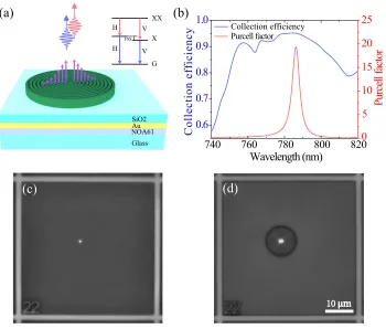
FIG. 1: Circular Bragg resonator on highly-efficient broadband reflector (CBR-HBR) for entangled-photon pair generation. Realization and calculated performance of the CBR-HBR are presented. (a) An illustration of a CBR-HBR with a single QD emitting entangled-photon pairs. The inset shows the XX-X cascaded radiative process for generating polarization-entangled photon pairs, in which the value of the fine structure splitting (FSS) plays an important role in determining the achievable entanglement fidelity without time-filtering. (b) Simulated Purcell factor (red) and collection efficiency (blue) of the CBR-HBR as a function of wavelength. The collection efficiency is based on a 40◦azimuth angle, corresponding to a numerical aperture (NA)=0.65. (c) and (d) are fluorescence images of the same QD before and after the fabrication of the CBR-HBR. (c) and (d) share the same scale bar.
Here we take a further step towards entangled photon pair sources with high brightness and indistinguishability by com-bining GaAs QDs with new broadband photonic nanostruc-tures, i.e., circular Bragg resonators on highly-efficient broad-band reflectors (CBR-HBR). Using a wide-field QD posi-tioning technique24,31,35, we deterministically fabricate
CBR-HBRs in which single GaAs QDs (see S.I. I) are precisely located at the optimal position (the center of the cavity) for high-performance entangled photon pair generation. A single-photon collection efficiency of up to 0.85(3) for both X and XX is achieved, resulting in a record photon pair collection probability of 0.65(4) per excitation pulse. A high degree of single-photon purity of 99.8(1)%, entanglement fidelity of 0.88(2), and indistinguishabilities of 0.901(3) and 0.903(3) are also simultaneously obtained.
Design and fabrication of devices
In order to realize bright entangled photon pairs with Purcell-enhanced emission rates, we have developed a new
nanostructure, i.e., CBR-HBR, with a few significant advan-tages respective to our previous work31. Most notably, the implementation of the HBR strucuture effectively suppresses the downwards photon leakage and therefore significantly im-proves the collection efficiency over a broadband, see the de-tails in the S.I. II. Our CBR-HBR consists of a circular Al-GaAs disk surrounded by a set of concentric AlAl-GaAs rings, sitting on a SiO2layer with a gold back reflector, as
schemat-ically shown in Fig. 1(a). The cavity resonance can be ac-curately engineered by varying the diameter of the central AlGaAs disk. Meanwhile, the in-plane emission is directed upwards by the concentric rings that meet the second-order Bragg conditions. By carefully designing the thickness of the SiO2insulator layer, all the photons leaking into the substrate
(a)
(b)
(c)
(d)
X_slab
XX_slab
-6 -3 0 3 6
0 0.01 0.02
Delay (ns)
0 13 -13
-26
-39 26 39
Delay (ns)
N
orm
al
iz
ed c
ount
s
N
orm
al
iz
ed c
ount
s
N
orm
al
iz
ed c
ount
s
0 0.2 0.4 0.6 0.8 1.0 1.2
Delay (ns) 0
0 0
0.2 0.4 0.6 0.8 1.0
0.2 0.4 0.6 0.8 1.0
0.4 0.8 1.2 1.6 2.0 Wavelength (nm)
760 765 770 775 780
0 0.2 0.4 0.6 0.8 1.0
36(18) ps X in slab XX in slab
X in CBR-HBR
XX in CBR-HBR
X_CBR-HBR
XX_CBR-HBR
Pulse area ( )
0.6
0
0 0.250.50.75 1 1.251.51.75 1.2
1.8 2.4 3.0 3.6
A
P
D
c
ount
s (M
H
[image:4.612.135.485.53.333.2]z)
FIG. 2:Basic characterization of the QD-CBR-HBR device.(a) PL spectrum of a QD in the CBR-HBR under two-photon resonant excitation (right y axis, indicated in red) and the cavity mode measured from white light reflection (left y axis, indicated in blue). The excitation power is chosen to maximize the intensity of the XX emission (”πpulse” conditions), X and XX are equally populated and resonant with the cavity mode of the CBR-HBR. (b) PL lifetime of X and XX in bulk and in the CBR-HBR, showing pronounced Purcell enhancement for both X and XX. (c) Photon auto-correlation measured under ”πpulse” two-photon resonant excitation, using a Hanbury-Brown and Twiss interferometer. The second-order correlationg(2)(0) =0.001±0.001 for X andg(2)(0) =0.007±0.001 for XX are calculated from the integrated area in the zero delay peak divided by the mean of the peaks away from zero-delay, and the uncertainty is a one standard deviation value. (d) Detected count rates of the X photons as a function of square root of the excitation power. The blue curve is a guide to the eyes.
90 % can be theoretically achieved in a bandwidth of≈33 nm, and Purcell factors above 2 can be obtained for a bandwidth of≈13 nm, which is 6.5 times the X-XX separation (≈2 nm).
We have developed a membrane transfer technique to re-alize the AlGaAs/SiO2/Au material platform from which
the CBR-HBRs are fabricated, with the details provided in the S.I. IV. We note that the presented photonic design is fully compatible with state-of-the-art piezoelectric-based tun-ing methods36–38, which enable the elimination of the FSS and the tuning of photon energy because of the flexible choice of substrate (here quartz) and flat morphology, which allows efficient strain transfer. By taking advantage of our recently developed QD positioning technique, we are able to identify individual QDs and extract their spatial positions with respect to alignment marks with an uncertainty of≈10 nm31,35, see Fig. 1(c). The CBR-HBR is then deterministically fabricated around the target QD. Figure 1(d) shows the fluorescence im-age of our device after the CBR-HBR fabrication, in which the targeted single QD in Fig. 1(c) is accurately located in the center of the fabricated CBR-HBR.
I. SINGLE-PHOTON EMISSION AND BRIGHTNESS
ASSESSMENT
Figure 2(a) presents the photoluminescence (PL) and white light reflectivity (1/R is shown, with R the reflectivity spec-trum) of our device at 3.2 K, see the optical setup in S.I. V. Under a pulsed two-photon resonant excitation (TPE) scheme16,20,21,38,39, the intensities of the XX and X
4
spectral match to the cavity mode, which enables faster trig-gering rates of entangled photon pair emission compared to those of the QDs in bulk.
Second-order auto-correlation measurements are per-formed for both X and XX, see Fig. 2(c). The nearly com-plete absence of coincidence events at zero time delay in-dicates the ultra-high purity of the emitted single-photons. g(X2)(0) =0.001(1)andg(X2)(0) =0.007(1)are obtained with-out background correction. The slightly higherg(X X2)(0)value of XX is mostly due to the very weak emission from neigh-boring QD states.
Different from the single-photon Rabi oscillation in which the population of the excited state is dependent on the pulse area, the pulse area in the two-photon Rabi oscillation is re-placed by an adiabatic dynamic phase that turns out to be a non-trivial function of the quantum dot binding energy, pulse area, pulse duration and pulse shape40. Fig. 2(d) shows the de-tected photon flux from X as a function of the square root of the time-averaged excitation power. The Rabi oscillations of X and XX (not shown) are observed due to the coherent con-trol of the two-level system consisting of the biexciton and crystal-ground-state in the QD. For this device, the photon count rate reaches a maximum for an average laser power of 36 nW, which we denote as ”πpulse” condition, similar to re-cent reports16,21. We note that the laser power needed to reach ”πpulse” for the QDs in a CBR-HBR is at least 200 times lower than that for QDs in the bulk and also in simple pla-nar cavities. Such a reduction of ”πpulse” power is attributed to the cavity enhanced excitation41 and represents an
advan-tage for filtering the excitation laser in the entanglement and indistinguishability measurements we shall present.
For a ”π pulse”, we observe a photon count rate up to 3.4(1) MHz under a 79 MHz repetition rate laser excitation. By taking the setup efficiencyξ(7 %, see S.I. VII ), avalanche photodiode (APD) correction factor (1.25), and XX prepara-tion fidelityηX X (≈0.9) into account, a collection efficiency (with a 0.65 NA objective)η=85(3) % is extracted for both X and XX. Consequently, the collected photon pair probability per pulsep=ηX X×η2×[1−gX(2)(0)]1/2×[1−g
(2)
X X(0)]1/2= 0.65(4) is obtained. This high photon pair rate per pulse p≈0.65 outperforms any of the existing entangled photon sources reported in the literature.
Entanglement characterization
The states of the photon pairs emitted by QDs can be writ-ten as |ψi=1/√2(|HXHX Xi+eisτ/~|VX XVXi)16,20,21,42, in whichτis the, statistically varying, decay time of the XX state relative to the decay time of the X state and s is the value of the FSS. In absence of other dephasing mechanisms, the devi-ation of the two-photon states from the Bell state|ψ+i
origi-nates from the phase factorsτ/~, which has to be minimized
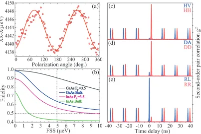
in order to obtain high level of entanglement without resorting to inefficient time-filtering43 or spectra-filtering14. Since the X lifetimeτX is as short as 60 ps in our device thanks to the Purcell effect (corresponding to a lifetime-limited linewidth of
∼11µeV), we expect that the generation of photon pairs with high time-averaged fidelity is still possible for QDs with a fi-nite FSS. Using polarization-dependent measurements, shown in Fig. 3(a), a FSS of 4.8(2)µeV for the QD in the CBR-HBR is extracted by subtracting the X transition from the XX tran-sition energy. The theoretical values of fidelity44as a function of FSS for different QDs with varied lifetimes are plotted in Fig. 3(b) (see the details in S.I. VIII). For GaAs QDs with a Purcell factor of 3.5, the entanglement fidelity decays slowly with the increase of the FSS. The predicted fidelity for the GaAs QDs with a FSS of 4.8µeV is as high as 0.92 and it can still be above 0.75 for a FSS of 10µeV. On the contrary, the en-tanglement fidelity for GaAs QDs in bulk (lifetime of 210 ps) decreases much more quickly with the increase of the FSS and shows a slightly lower value than the Purcell-enhanced source at FSS=0. With the same FSS of 4.8ueV, the entanglement fi-delity is only 0.64 for GaAs QDs in bulk. In order to compare the performance against a different material system, we also plot the entanglement fidelities of Purcell-enhanced InAs QDs (Fp=3.5) and InAs QDs in bulk (typical lifetime of 1000 ps). For the InAs QDs in bulk, the highest fidelity is<0.75 and the entanglement disappears once the FSS is larger than 1.6µeV. Even with the same Purcell factor of 3.5, the entanglement fi-delity of InAs QDs is still not reaching to the level of GaAs QDs in bulk. These results are based on the spin-scattering times provided in Ref. 20,21 and need further experimental confirmations.
To evaluate the degree of entanglement of our bright photon-pair source, we perform cross-correlation measure-ments underπ pulse excitation for both X and XX photons in linear (HV), diagonal (DA), and circular (LR) basis sets. The cross-correlation histograms in the three basis sets are presented in Fig. 3(c-e). In linear and diagonal basis sets, we clearly observe the antibunching when the photon pairs are co-polarized and bunching for the cross-polarized photon pairs. The correlation in the circular basis is just opposite: co-polarized photon pairs show bunching while cross-co-polarized ones exhibit antibunching behavior. This set of correlations serves as a strong indication of polarization entanglement in the photon pairs. The degree of correlation in a particular po-larization basis is defined by44:
Cµ=
g(X X,X2) (0)−g(X X,2) ¯ X(0)
g(X X,X2) (0) +g(X X,2)X¯(0)
whereg(X X,X2) (0)andg(X X,2)X¯(0)are the second order correlation for the co-polarized and cross-polarized photon pairs in that basis at zero delay time. The extracted degree of correlation in the different basis sets from measured coincidence histograms are:
Clinear=0.92(2)
0 60 120 180 240 300 360 4138
4140 4142 4144 4146 4148 4150
0 1 2 3 4 5 6 7 8 9 10 0.4
0.5 0.6 0.7 0.8 0.9 1.0
-40 -30 -20 -10 0 10 20 30 40
(c)
(b)
2
X
X
-X
(
µ
eV
)
Polarization angle (deg.)
(a)
(d)
(e)
H HVV
H HHH
F
ide
li
ty
FSS ( eV)
GaAs Fp=3.5 GaAs Bulk
InAs Bulk
InAs Fp=3.5
DA
D DDD
Time delay (ns)
R
RLL
R RRR
S
ec
ond-orde
r pa
ir c
orre
la
ti
[image:6.612.107.510.51.321.2]on g
FIG. 3:Entanglement characterization. Fidelity of the polarization entanglement is investigated. (a) Polarization-dependent measurement to determine the FSS of X. The relative energy difference between X and XX is plotted in order to obtain a higher measurement precision. An FSS value of 4.8(2)µeV is extracted from the amplitude of the sine-function fitting. (b) Theoretically predicted entanglement fidelity as a function of FSS for GaAs QDs in the CBR-HBR (Fp=3.5, black line), in bulk (blue line), Purcell enhanced InAs QDs (Fp=3.5, ruby line)
and InAs QDs in bulk (green line). The vertical dashed line denotes a FSS of 4.8µeV and the horizontal dashed line (f=0.5) is the boundary above which quantum entanglement exists. (c), (d) and (e) are the X-XX polarization dependent cross-correlation histogram under ”πpulse” conditions for linear, diagonal, and circular basis respectively. Data for cross-polarization configurations are shifted deliberately for clarity.
With these numbers, the entanglement fidelity for the polar-ization between the emitted photon pairs can be calculated as:
f =1+Clinear+Cdiagonal−Ccircular
4 =0.88(2)
The theoretically predicted entanglement fidelity of 0.92 can be reduced to 0.88 by using a much shorter spin scattering time (1 ns instead of 15 ns), which strongly indicates the ex-istence of extra dephasing processes. Such extra dephasing processes have been also recently observed in a similar ma-terial system and is attributed to the interactions between the confined exciton and charge states38. In contrast to existing entangled sources with vanishing FSS, the pronounced Pur-cell effect in our work makes the high fidelity of entanglement possible for QDs with a comparatively large FSS. A near-unity entanglement fidelity can be expected in the future by implementing GaAs QDs with very small FSS in CBR-HBRs or by eliminating the residual FSS with a strain-tunable CBR-HBR38(see strain-tunable CBR-HBR in the S.I. IX).
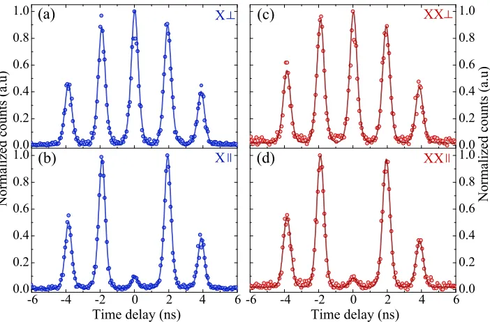
Photon indistinguishability
Photon indistinguishablity is a prerequisite for the real-ization of long-haul quantum information processing, e.g., a
quantum repeater via entanglement swapping45. We study the
6
0.0 0.2 0.4 0.6 0.8 1.0
0.0 0.2 0.4 0.6 0.8 1.0
-6 -4 -2 0 2 4 6
0.0 0.2 0.4 0.6 0.8 1.0
-6 -4 -2 0 2 4 60.0
0.2 0.4 0.6 0.8 1.0
XX
X
XX
X
N
orm
al
iz
ed c
ount
s (a
.u)
N
orm
al
iz
ed c
ount
s (a
.u)
Time delay (ns) Time delay (ns)
(a)
(b)
(c)
[image:7.612.134.485.50.281.2](d)
FIG. 4: Photon indistinguishability. HOM interference for X and XX photons are performed individually. Two-photon interference for cross-polarized (a), co-polarized (b) X photons and cross-polarized (c), co-polarized (d) XX photons. The data are fitted by exponential decays (measured emitter decay response) convolved with a Gaussian (measured photon detector time response). The area of the central peaks is extracted to calculate the raw visibilities, which are 0.901(3) and 0.903(3) for X and XX respectively.
TABLE I: Characterization of more devices from the same chip.
Device# Single-photon effi-ciency/Pair rate
Cavity wavelength (nm) X wavelength (nm) X Purcell factor FSS (µeV)/f X HOM XX HOM
1 0.86/0.65 772.43 770.05 3.5 4.8/0.88 0.9 0.9
2 0.80 769.36 770.86 2.6 11.6/N.A. N.A. N.A.
3 0.76 767.39 777.51 3.1 18.0/N.A. N.A. N.A.
4 0.70/0.44 767.18 778.91 3.1 3.4/0.85 0.81 0.84
5 0.67 766.17 767.08 1.7 5.8/N.A. N.A. N.A.
6 0.66 763.86 765.08 2.1 11.0/N.A. N.A. N.A.
7 0.63 766.76 766.18 2.7 9.1/N.A. N.A. N.A.
8 0.61 767.20 770.20 3.4 5.1/N.A. N.A. N.A.
9 0.56 765.53 769.51 2.2 15.8/N.A. N.A. N.A.
10 0.55 764.24 766.62 2.0 6.6/N.A. N.A. N.A.
histogram. We note that the high degree of photon indistin-guishability in our pair source is a direct result of the Purcell effect, which has been recently shown as a key element to realizing highly indistinguishable single-photons from InAs QDs in micropillar cavities22–24. With a joint force of further improvement of the Purcell factor, charge-stabilization23,47 and rapid adiabatic passage excitation48, higher photon
in-distinguishability can be expected as well as the entangle-ment fidelity. However, in our devices, the collection effiency tends to decrease with higher Q-factors (therefore higher Pur-cell factors) of the cavity due to the reduction of the overlap between the far-field pattern and the objective. Ultimately, the simultaneous realization of high collection efficiency and high indistinguishability will be fundamentally limited by the phonon scattering process. An upper bound can be placed on the indistinguishability by considering the microscopic theory developed in Ref. 49. This theory uses the polaron master
equation formalism to capture non-Markovian phonon pro-cesses that lead to the emergence of a phonon sideband in the QD emission spectrum, and consequently degrades the indis-tinguishability of the source. Using this formalism with stan-dard GaAs parameters, we find that our source could have an indistinguishability as high as 0.98 in the absence of any other dephasing processes (e.g. charge noise), see the S.I. X for details of the calculation. However, moderate filtering of the phonon sidebands (at the expense of a few percent count re-duction) may be used to further boost the indistinguishability.
[image:7.612.68.548.373.509.2]TABLE II: Comparison of the performance of our device to the state-of-the-art entangled sources.
Pair efficiencyaEntanglement Fidelity Indistinguishability
InAs QD in micropillar molecule (Ref 32) 0.12 0.63 Not shown
InAsP QDs in nanowires (Ref 33) 0.0025 0.817 Not shown
InAs QDs in planar cavities (Ref 16) <0.0001 0.81 0.86
GaAs QDs in planar cavities (Ref 21) <0.0001 0.94 0.93
SPDC USTC (Ref 10) ∼0.1 0.93 0.91
SPDC Vienna (Ref 2) <0.01 >0.95 >0.9
SPDC Geneva (Ref 9) <0.1 ∼0.9 ∼0.9
This work 0.65(4) 0.88(2) ∼0.9
aThe photon pair source efficiency is defined by the probability of collecting a photon pair per excitation
pulse into the first collection optics, such as an objective or an optical fiber.
of 3.4µeV and the device 1 has the second smallest FSS of 4.8µeV with the highest Purcell factor of 3.5. Therefore we do not expect any higher entanglement fidelity in the other de-vices. The limiting factor of the entanglement fidelity in this batch of devices is the relative large FSSs of the GaAs droplet QDs grown in the thin membrane (140 nm) structure with a thick sacrificial layer (500 nm), as shown in Fig. S1(a). We believe such a limitation can be soon overcome by either opti-mizing the epitaxial growth process or developing the strain-tunable CBR-HBR that we proposed.
Summary
Given the rapid development of the entangled photon sources both with SPDC and QD technologies, it is very in-sightful to directly compare the performance of our device to those of the existing sources reported in the literature. Table 2 lists the efficiency, entanglement fidelity, and indistinguisha-bility of the state-of-the-art entangled photon sources together with our device (reference S.I. XII for methodology used in extracting the various parameters.). In general, the SPDC sources exhibit excellent performance in terms of entangle-ment fidelity and photon indistinguishability; however, their efficiencies are intrinsically limited to<0.1 due to the nature of the Poissonian statistics. Increasing the photon pair flux through higher excitation power inevitably adds extra noise and reduces the purity and indistinguishability. For the de-terministic approach, the efficiency of QDs in bulk suffers greatly from the total internal reflection and only a few works show a high-degree of indistinguishability. InAsP QDs in nanowires and InAs QDs in micropillar molecules show much improved brightness and decent entanglement fidelity, but still the source efficiency and indistingshability have to be further improved. Our device, for the first time, simultaneously com-bines a high pair collection probability (0.65(4)), high degree of entanglement fidelity (0.88(2)) and photon indistinguisha-bility (0.901(3) and 0.903(3)), and when taken together
out-performs all the existing entangled photon pair sources. To conclude, we have implemented a broadband photonic nanostrucuture, CBR-HBR, to harvest highly-entangled pho-ton pairs emitted by GaAs QDs, obtained by droplet etch-ing. By employing the QD positioning technique based on fluorescence imaging, the QDs are accurately placed in the center of the CBR-HBR, thus enabling the realization of en-tangled sources with record performances. Our devices may immediately find applications in both fundamental physics and applied quantum technologies, e.g., quantum random walk with entangled photon pairs50, generation of hyper-entanglement51and quantum repeaters6associated with quan-tum memories. Moving forward, realizing high-performance photon pair sources operating in the telecom band52,53is par-ticularly appealing for long-haul quantum communication. In-stead of polarization entanglement, time-bin entanglements39 can be directly generated from QDs, which makes our de-vices compatible with the fiber network. The operation wave-length for both droplet QDs and photonic nanostructures can be shifted to the telecom band by changing the filling material of the nanohole and scaling the size of the nanostructures. To scale this technology up to multiple QDs, piezo-tuning36,37or on-chip quantum frequency conversion technologies54can be directly implemented in our devices to tune the QD emission wavelength, overcome the spectral inhomogeneity between different QDs and eliminate the FSS. Such identical entangled pair sources can serve as individual nodes interconnected via single-photon interference in the future quantum network55. With the potential of scalability, our work serves as a land-mark in the development of semiconductor quantum informa-tion processing chips and may boost new breakthroughs in quantum photonic technologies.
References
∗ These authors contributed equally
† Correspondence to [email protected],
Quantum-8
Mechanical Description of Physical Reality Be Considered Com-plete?, Phys. Rev.47, 777 (1935).
2 Giustina, M., et al. Significant-Loophole-Free Test of Bell’s
The-orem with Entangled Photons. Phys. Rev. Lett. 115, 250401 (2015).
3 Shalm, L. K., et al. Strong Loophole-Free Test of Local Realism.
Phys. Rev. Lett.115, 250402 (2015).
4 Bouwmeester, D., Ekert, A. K., and Zeilinger, A. The Physics of
Quantum Information(Springer, 2000).
5 Kimble, H. J. The Quantum Internet.Nature453, 1023 (2008). 6 Simon, C., et al. Quantum Repeaters with Photon Pair Sources
and Multimode Memories.Phys. Rev. Lett.98, 190503 (2007).
7 Acin, A., et al. Device-Independent Security of Quantum
Cryp-tography against Collective Attacks. Phys. Rev. Lett.98, 230501 (2007).
8 Kwiat, P. G., et al. New High-Intensity Source of
Polarization-Entangled Photon Pairs.Phys. Rev. Lett.75, 4337 (1995).
9 Scarani, V., Riedmatten, H. De, Marcikic, I., Zbinden, H., and
Gisin, N. Four-photon correction in two-photon bell experiments.
The European Physical Journal D-Atomic, Molecular, Optical and Plasma Physics32, 129 (2005).
10 Wang, X. L., et al. Experimental Ten-Photon Entanglement.Phys.
Rev. Lett.117, 210502 (2016).
11 Pan, J. W., et al. Multiphoton entanglement and interferometry.
Rev. Mod. Phys.2012, 072501 (2012).
12 Benson, O., Santori, C., Pelton, M., and Yamamoto, Y. Regulated
and Entangled Photons from a Single Quantum Dot. Phys. Rev. Lett.84, 2513 (2000).
13 Young, R. J., et al. A semiconductor source of triggered entangled
photon pairs.New J. Phys.8, 29 (2006).
14 Akopian, N., et al. Entangled Photon Pairs from Semiconductor
Quantum Dots.Phys. Rev. Lett.96, 130501 (2006).
15 Muller, A., Fang, W., Lawall, J. and Solomon, G S. Creating
polarization-entangled photon pairs from a semiconductor quan-tum dot using the optical Stark effect. Phys. Rev. Lett. 103, 217402 (2009).
16 M¨uller, M., Bounouar, S., J¨ons, K. D., Gl¨ass, M. and
Mich-ler, P. On-demand generation of indistinguishable polarization-entangled photon pairs.Nat. Photon.8, 224 (2014).
17 Chung, T. H., et al. Selective carrier injection into patterned arrays
of pyramidal quantum dots for entangled photon light-emitting diodes. Nat. Photon.10, 782 (2016).
18 Orieux, A., Versteegh, M. A. M., J¨ons, K. D. and Ducci, S.
Semi-conductor devices for entangled photon pair generation: a review.
Rep. Prog. Phys.80, 076001(2017).
19 Huo, Y. H., Rastelli, A. and Schmidt, O . G. Ultra-small excitonic
fine structure splitting in highly symmetric quantum dots on GaAs (001) substrate.Appl. Phys. Lett.102,152105 (2013).
20 Keil, R., et al. Solid-state ensemble of highly entangled photon
sources at rubidium atomic transitions. Nat. Commun.10, 15501 (2017).
21 Huber, D., et al. Highly indistinguishable and strongly entangled
photons from symmetric GaAs quantum dots.Nat. Commun.10, 15506 (2017).
22 Ding, X., et al. On-demand single photons with high extraction
efficiency and near-unity indistinguishability from a resonantly driven quantum dot in a micropillar.Phys. Rev. Lett.116, 020401 (2016).
23 Somaschi, N., et al. Near-optimal single-photon sources in the
solid state.Nat. Photon.10, 340-345 (2016).
24 He, Y.-M., et al. Deterministic implementation of a bright,
on-demand single-photon source with near-unity indistinguishability via quantum dot imaging.Optica4, 802-808 (2017).
25 Claudon, J., et al. A highly efficient single-photon source based
on a quantum dot in a photonic nanowire. Nat. Photon.4, 174 (2010)
26 Reimer, M. E., et al. Bright single-photon sources in bottom-up
tailored nanowires.Nat. Commun.3, 737 (2012)
27 Laucht, A., et al. A Waveguide-coupled On-Chip Single-Photon
Source.Phys. Rev. X2, 011014 (2012).
28 Arcari, M., et al. Near-unity coupling efficiency of a quantum
emitter to a photonic crystal waveguide. Phys. Rev. Lett.113, 093603 (2014).
29 Gschrey, M., et al. Highly indistinguishable photons from
deter-ministic quantum-dot microlenses utilizing three-dimensional in situ electron-beam lithography.Nat. Commun.6, 7662 (2015).
30 Davanco, M., Rakher, M. T., Schuh, D., Badolato, A. and
Srini-vasan, K., A circular dielectric grating for vertical extraction of single quantum dot emission.Appl. Phys. Lett.99, 041102 (2011).
31 Sapienza, L., Davano, M., Badolato, A. and Srinivasan, K.
Nanoscale optical positioning of single quantum dots for bright and pure single-photon emission.Nat. Commun.6, 7833 (2015).
32 Dousse, A., et al. Ultrabright source of entangled photon pairs.
Nature466, 217 (2010).
33 J¨ons, K. D., et al. Bright nanoscale source of deterministic
en-tangled photon pairs violating Bells inequality.Sci. Rep.7, 1700 (2017).
34 Chen, Y., Zopf, M., Keil, R., Ding, F. and Schmidt, O. G.
Highly-efficient extraction of entangled photons from quantum dots using a broadband optical antenna.Nat. Commun.9, 2994 (2018).
35 Liu, J., et al. Cryogenic photoluminescence imaging system for
nanoscale positioning of single quantum emitters. Rev. Sci. In-strum.88, 023116 (2017).
36 Chen, Y., et al. Wavelength-tunable entangled photons from
silicon-integrated IIIV quantum dots. Nat. Commun.7, 10387 (2016).
37 Trotta, R., et al. Wavelength-tunable sources of entangled photons
interfaced with atomic vapors.Nat. Commun.7, 10375 (2016).
38 D. Huber et al. Strain-tunable GaAs quantum dot: An on-demand
source of nearly-maximally entangled photon pairs. Phys. Rev. Lett.121, 033902 (2018).
39 Jayakumar, H., et al. Time-bin entangled photons from a quantum
dot.Nat. Commun.5, 4251 (2014).
40 Stufler, S., et al. ”Two-photon Rabi oscillations in a single
InxGas1−xA/GaAs quantum dot,” Phys. Rev. B 73, 125304
(2006).
41 Kaniber, M., et al. Efficient and selective cavity-resonant
exci-tation for single photon generation. New J. Phys.11, 013031 (2009).
42 Stevenson, R. M., et al. Evolution of Entanglement Between
Dis-tinguishable Light States.Phys. Rev. Lett.101, 170501 (2008).
43 Ward, M. M., et al. Coherent dynamics of a telecom-wavelength
entangled photon source.Nat. Commun.5, 3316 (2014).
44 Hudson, A. J., et al. Coherence of an Entangled Exciton-Photon
State.Phys. Rev. Lett.99, 266802 (2007).
45 Duan, L. M., Lukin, M. D., Cirac, J. I. and Zoller, P.
Long-distance quantum communication with atomic ensembles and lin-ear optics.Nature414, 413 (2001).
46 Santori, C., Fattal, D., Vuckovic, J., Solomon, G. S. and
Ya-mamoto, Y. Indistinguishable photons from a single-photon de-vice.Nature419, 594 (2002).
47 Liu, J., et al., Single Self-Assembled InAs/GaAs Quantum Dots
in Photonic Nanostructures: The Role of Nanofabrication. Phys. Rev. Appl.9, 064019 (2018).
48 Kaldewey, T., et al. Coherent and robust high-fidelity generation
of a biexciton in a quantum dot by rapid adiabatic passage.Phys. Rev. B95, 161302(R) (2017).
Phonon scattering inhibits simultaneous near-unity efficiency and indistinguishability in semiconductor single-photon sources.Nat. Photon.11, 521 (2017).
50 Pathak, P. K. and Agarwal, G. S. Quantum random walk of
two photons in separable and entangled states. Phys. Rev. A75, 032351 (2007).
51 Prilm¨uller, M., et al. Hyperentanglement of Photons Emitted by
a Quantum Dot.Phys. Rev. Lett.121110503 (2018).
52 Olbricha, F., et al. Polarization-entangled photons from an
InGaAs-based quantum dot emitting in the telecom C-band.Appl. Phys. Lett.,111, 133106 (2017).
53 Huwer, J., et al. Quantum-Dot-Based
Telecommunication-Wavelength Quantum Relay.Phys. Rev. Appl.8, 024007 (2017).
54 Li, Q., Davanc¸o, M. and Srinivasan, K. Efficient and low-noise
single-photon-level frequency conversion interfaces using silicon nanophotonics.Nat. Photon.10, 406 (2016).
55 Gao, W. B., et al. Quantum teleportation from a propagating
pho-ton to a solid-state spin qubit.Nat. Commun.11, 2744 (2013)
Acknowledgements
We acknowledge R. Trotta, X. Yuan, H. Huang, M. Reindl, D. Huber and Y. Huo for very fruitful discussions. We are greatful to the financial supports from the Na-tional Key R&D Program of China (2016YFA0301300, 2018YFA0306100), the National Natural Science Foun-dations of China (91750207, 1133405, 11674402, 11761141015, 11761131001, 11874437), Guangzhou Science and Technology project (201607020023, 201805010004), the Natural Science Foundations of Guangdong (2018B030311027, 2016A030312012), and the Austrian Science Fund (FWF): P29603.
Author Contributions
R. B. S, J. T. L and X. H. W conceived the nanostructure and its fabrication strategy. J. L designed the measurement scheme. R. B. S and K. S contributed to the structure simula-tions. S. F. CdS and Y. Y grew the quatum dot wafers. R. B. S, B. M. Y, J. T. L and J. L fabricated the devices. Y. M. W, R. B. S, B. M. Y and J. L characterized the devices. J. I. S performed the indistinguishability calculation. J. L, Y. M. W, and R. B. S analyzed the data. J. L wrote the manuscript with inputs from all authors. J. L, A. R and X. H. W supervised the project.
Competing financial interests
The author declare that they have no competing financial in-terests.
Data availability statement
The data that support the plots within this paper and other find-ings of this study are available from the corresponding author upon reasonable request.
Additional information
Supplementary informationis available in the online ver-sion of the paper.
Reprints and permission informationis available online at www.nature.com/reprints.
Correspondence and requests for materialsshould be ad-dressed to A. S, J. T, L or X. H. W.
Methods Simulation
The numerical simulaitons are carried out by means of finite-difference time-domain method, using a commercial software, Lumerical FDTD solutions. An electrical dipole is placed in the center of the CBR-HBR structure and six power monitors emcompassing the structure are employed to record power emitted by the dipole source. The sum power transmission normalized to that of the same source in homogeneous materi-als is calculated as the Purcell factor. The electric field record by the top monitor is used to calculate the far-field pattern by means of near-field to far-field projection. The collection efficiencies are extracted from the far-field distribution in 40 degree corresponding to N.A. of 0.65 (for further details see S.I. section II).
Fabrication
The epi-structure of the wafer is schematically shown in S.I. I. After cleaning with acetone and isopropanol, 220 nm SiO2
layer and 100 nm Au layer are deposited on the wafer by in-ductively coupled plasma chemical vapor deposition (Oxford instruments, PlasmaPro System100 ICP180-CVD) and elec-tronic beam evaporation (Wavetest, DE400) repectively. The wafer is bonded to a glass substrate via ultraviolet curing re-sist (Norland, NOA 61). After exposure, the wafer is placed in a 50◦C thermostat for 24 hours aging process to get an op-timized performance. The original GaAs substrate is removed with phosphoric acid (H 2PO4:H2O2:H2O = 1:1:1 volume)
for 1.5 hour and selective etching solution (citric acid:H2O2
= 3:1 volume) until stopping at the sacrificial layer. The Al0.8Ga0.2As sacrificial layer is removed with 10% HF. The
CBR-HBR structures are defined by an electron beam lithog-raphy(Vistec EBPG5000+ system). The alignment marks (10 nm Ti and 100 nm Au) are patterned with an electron beam lithography and a lift-off process. An Ar-SiCl4based
dry etching process(Oxford instruments, PlasmaPro System 100 ICP180) is used to etch the GaAs structure.
Two-photon resonant excitation