International Journal of Innovative Technology and Exploring Engineering (IJITEE) ISSN: 2278-3075, Volume-8 Issue-7 May, 2019
Abstract: Vedic science is an antiquated strategy of Indian arithmetic as it contains 16 Sutras. A fast 16 *16 multiplier configuration is designed utilizing Urdhva Tiryakbhyam sutra is introduced in this work. By utilizing this sutra the fractional items and entireties are created in single stage which decreases the structure of design in processors. By utilizing this method we can diminish the delay to the maximum extent when contrast with cluster or corner multiplier. By utilizing this strategy we lessen the inciting delay in connection with bunch based plan and parallel carry based use which are most normally used models. The essential significance of this paper is the delay and dynamic power usage is found to be diminished.
Keywords: Wallace tree multiplier, Vedic multiplier (VM), Reversible logic
I. INTRODUCTION
Augmentation is a central capacity in math activities dependent on several tasks. Adders form the fundamental basic structure of the multiplier. Generally subtraction is a two‟s complement addition. These arithmetic operations should be performed in the fastest manner for high speed applications. Once these operations are performed in high speed, then they can be used to speed up the operations of the complicated circuits. So designing the efficient adder is in the front line. Further due to the advancement in the technology, several parameters like wire length, number of fan outs are also taken into account. Reversibility in processing suggests that no data about the computational states can ever be lost, so we can recoup any prior stage by registering in reverse the outcomes. This is named as logic reversibility. The condition of inputs can be recuperated from the outputs by using the concept of reversible logic components. This reversible logic is used in adders and reversible adders are designed. The adder block in the Vedic multiplier are replaced by this reversible adders to form the reversible Vedic multiplier (VM). This proposed Reversible VM proved to be the best when compared with the existing Wallace tree multiplier and conventional VM in terms of delay and power consumption.
Revised Manuscript Received on May 10, 2019
S.Prema, Department of ECE, SNS College of
Technology,Coimbatore,Tamil Nadu,India.
Ramanan.S.V, Department of ECE, PPG Institute of
Technology,Coimbatore,Tamil Nadu,India.
R.Arun Sekar, Department of ECE, GMR Institute of
Technology,Rajam,Andhra Pradesh,India.
Rajan Cristin, Department of CSE, GMR Institute of
Technology,Rajam,Andhra Pradesh,India.
The operation and functionality of Wallace tree multiplier is described in the section II. VM methodology is described in the section III. The proposed reversible VM is described in the section IV. Implementation of proposed method in Cadence 45nm technology is explained in the section V. The result discussion for this work is explained in the section VI.
II. WALLACEMULTIPLIER
Eminent quick multipliers are Wallace multiplier [1,2] which uses carry save adders to decrease N-sections of fragmented things to two line lattice. The carry save adders are standard full adders whose carry are not related, with the objective that three words are taken in and two words are yield. The Wallace multiplier uses half adders and full adders in their decrease arrange. Here a balanced framework is shown that altogether lessens the half adders. In Wallace multiplier, in the second step of decrease the Wallace approach uses a couple of periods of full adders and half adders as carry save adders. In the Wallace multiplier the incomplete item decrease arrange uses carry save adder. The quantity of full adders and half adders used are 50 and 20 individually. Four phases are required for decrease. In the middle of the road stages and the last carry propagate phase of standard Wallace tree multiplier, the Carry propagate adder is associated.
Figure 1 Schematic of Wallace multiplier
High Performance Reversible Vedic Multiplier
Using Cadence 45nm Technology
III. VEDICMATHEMATICS
The utilization of Vedic science is to decreases the regular figuring‟s in traditional science to exceptionally basic one. It additionally gives viable calculations that to be connected to different parts of designing, for example, registering.
A. Urdhva Tiryakbhyam Sutra
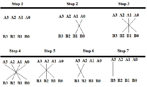
"Urdhva Tiryagbhyam" sutra is used in our proposed Vedic multiplier [3] . The augmentation of any two decimal formatted variables is performed by using this sutra. This sutra operates in both crosswise and vertical direction. This sutra is one among the 16 sutras and is based on the ancient vedic mathematics. Here all the partial products generation and the addition take place concurrently. Further this sutra is based on the addition equation which is utilized for the multiplication. Because of its normal schematic, it tends to be effectively format in microchips and planners can without much of a stretch bypass these issues to maintain a strategic distance from calamitous gadget disappointments. The Vedic multiplier (VM) module for different bits is explained as below.
B. VM for 2*2 piece Module
The operation of 2*2 VM where the 2-bit numbers X and Y are X = x1x0 and Y = y1y0. The minimum noteworthy bits are duplicated which gives the minimum huge piece of the last item (vertical). At that point, the multiplicand (LSB) is duplicated with the following multiplier upper piece and included with, the result of multiplier LSB and next multiplicand (across) Upper piece. The procedure goes on in a similar way.The operational structure of the two bit VM is given in the following equations.
p0 = x0y0; (1) z1p1 = x1y0 + x0y1; (2) z2p2 = z1 + x1y1; (3)
The last outcome will be z2p2p1p0. This augmentation strategy is appropriate for all the cases. Generally four AND gates and two HA are utilized for implementing 2*2 VM module. Even though it is similar to the conventional array multiplier, the main purpose of designing 2*2 VM is, it can be used for designing 4*4 VM and so on.
C. VM for 4*4 bit Module
The schematic diagram of 4*4 VM module is shown in the figure 2. The operation is similar to 2*2 VM module. In the equations represented below the two 4-bit binary numbers X3X2X1X0 and Y3Y2Y1Y0 multiplication. Due to this multiplication nearly 8 bits namely P0P1P2P3P4P5P6Z6 are produced as the output.
Figure 2 4*4 bit binary multiplication using Urdhva Tiryakbhyam
p0 = x0.y0 ……….. (4) z1p1 = x1y0 + x0y1 ………. (5) z2p2 = z1 + x1y1 + x2y0 + x0y2 ……….. (6) z3p3 = z2 + x3y0 + x0y3 + x1y2 + x2y1 ………. (7) z4p4 = c3 + x3y1 + x1y3 + x2y2 ………... (8) z5p5 = c4 + x3y2 + x2y3 ………. (9) z6p6 = c5 + x3y3 ………... (10)
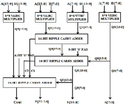
D. VM for 16*16 bit Module
16*16 VM is designed using four 8*8 VM and three 16-bit Ripple Carry Adder (RCA). Here X and Y are 16-bit binary numbers.
[image:2.595.316.559.52.197.2]International Journal of Innovative Technology and Exploring Engineering (IJITEE) ISSN: 2278-3075, Volume-8 Issue-7 May, 2019
Figure 3 Schematic diagram of 16x16 normal VM
IV. REVERSIBLEGATES
An n input and n output logic is utilized in reversible gate. The representation is called as one to one mapping. The outputs can be easily determined from the inputs meanwhile the inputs can also be obtained from the outputs. Since one to many concept is not reversible, direct fan out is not allowed during the synthesis of reversible circuits. Any how we can achieve the fan out in the reversible circuits by utilizing additional gates. While designing the reversible circuit we must keep an eye on using the number of reversible logic gates to be minimum. The complexity and the performance of the circuit are determined by number of factors.
A. BME Gate
BME is a 4*4 reversible gate. It has four inputs and four outputs. The information is given by i(A,B,C,D) and the response is represented by o(P,Q,R,S). The output is defined by P = A, Q = AB^C, R = A.D^ C and S = (A‟B^C^D).Figure 4 shows the block diagram of BME gate. Figure 5 shows the schematic of BME reversible gate.
[image:3.595.315.550.265.443.2][image:3.595.46.285.588.757.2]
Figure 4: Block diagram of Reversible BME gate
Figure 5: Schematic of Reversible BME gate
B. Peres Gate
One form of 3*3 reversible entryway is the Peres gate.It has three information sources and three output responses. The illustration of Peres entryway is indicated below in the Figure 6 and Figure 7 shows the schematic of reversible Peres gate by using Cadence tool. The response is given by A, Y=A^B, Z=AB^C. Peres gate has the Quantum cost of five.
Figure 6 Block diagram of Reversible Peres Gate
Figure 7 Schematic of Reversible Peres gate
V. REVERSIBLE2*2VM
Figure 8 Schematic diagram of Reversible 2*2 VM
Figure 9 Schematic of Reversible 16*16 Vedic multiplier
Schematic of Reversible 16*16 VM [8-11] is shown in Figure 9. Reversible 16*16VM is designed using multiple stages of 8x8 reversible VM which is constructed from 4x4 Reversible VM and so on. The first stage has only a single 8-bit Reversible VM. The 8-bit Reversible VM is built using two 4-bit Reversible VM where the 4- bit is built up by two 2-bit Reversible VM. Here the output of the first stage is the 16-bit output. The LSB of the output [7:0] is taken directly whereas the MSB [15:8] is fed to the Reversible RCA.
[image:4.595.88.494.59.263.2]International Journal of Innovative Technology and Exploring Engineering (IJITEE) ISSN: 2278-3075, Volume-8 Issue-7 May, 2019
uthor-1 Photo
[image:5.595.47.272.96.208.2]Author-2 Photo VI.RESULTSANDDISCUSSION
Table 1 Comparison of Different Multipliers
MULTIPLIER CELLS AREA TOTAL POWER(nW)
DELAY
(pS)
WALLACE
MULTIPLIER 3562 1873
2 7642414.8 12932
NORMAL
VM 736 7125 363926.99 6024
REVERSIBLE
VM 1945 9844 281869.6 5353
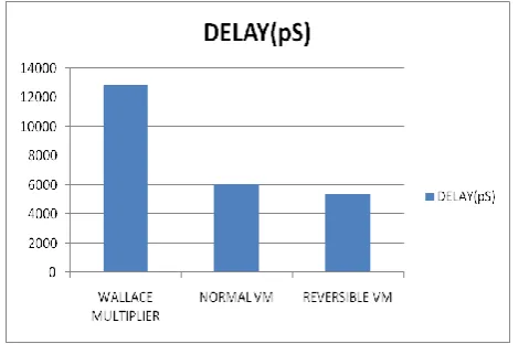
Table 1 shows the comparison result of different multipliers. It is generally noted that the VM has lowest delay and low power when compared to other types of multipliers. But when reversible logic is applied to this multiplier, it is seen that the power and delay are further reduced. The delay is reduced by 11.13% and the power is reduced by 22.54%. Figure 10(a) and Figure 10(a) shows the pictorial representation of the comparison result. Simulations are performed using Cadence 45nm technology.
Figure 10(a) Delay comparison of different multipliers
Figure 10(b) Power comparison of different multipliers
REFERENCES
1. Wallace C.S, “A Suggestion for a Fast Multiplier‟‟,IEEE Transactions on Electronic Computers‟, Vol.13,1964, pp. 14-17.
2. Waters R. S. et.al., “A Reduced Complexity Wallace Multiplier Reduction,” IEEE Transactions on Computers, vol. 59, 2010, pp. 1134-1137.
3. Sushma R.Huddar et.al., ‟Novel Vedic mathematics multiplier using compressors‟, International Mutli-Conference on Automation, Computing, Communication, Control and Compressed Sensing,2013. 4. Rakshith S, Rakshith T, „Optimized Reversible Vedic Multipliers for
low power operations‟ IEEE Conference on Information and communication Technologies, 2013.
5. Thapliyal, H and Srinivas, M, B, “Novel Reversible Multiplier Architecture Using Reversible TSG Gate”, Proceedings on IEEE International Conference on Computer Systems and Applications, 2006, pp. 100-103.
6. Shams, M, Haghparast, M and Navi, K, “Novel Reversible Multiplier Circuit in Nanotechnology”, World Applied Science Journal, Vol. 3, No. 5, 2008, pp. 806-810.
7. Koti lakshmi, Santhosh kumar and Rameshwar Rao, ‟Implementation of Vedic Multiplier Using Reversible Gates‟, International Conference on Computer science and Information Technology, 2015, pp 125-134. 8. Vijay K Panchal and Vimal H Nayak, ‟Analysis of multiplier circuit
using reversible logic „, International journal for Innovative Research in Science and Technology, Vol 1, Issue 6, Nov 2014.
9. Ratna Raju et.al.,‟ A High Speed 16*16 Multiplier Based on Urdhva Tiryakbhyam Sutra‟, International Journal of Science Engineering and Advance Technology, Vol 1, Issue 5,2013.
10. Vishikha Sharma, Aniket Kumar,‟‟ Design, Implementation & Performance of Vedic Multiplier for Different Bit Lengths‟, International Journal of Innovative Research in Computer and Communication Engineering, Vol. 5, Issue 4, April 2017.
11. R Arun Sekar, S Sasipriya, “Implementation of FIR filter using reversible modified carry select adder”, Concurrency and Computation: Practice and Experience, Sep.2018, pp. 1-9.
AUTHORSPROFILE
S. Prema working as an Assistant Professor in the Department of Electronics and Communication Engineering, SNS College of Technology, Coimbatore. She obtained her B.E in ECE from Hindusthan College of of Engineering and Technology, Coimbatore and M.E in VLSI Design from Sasurie College of Engineering Coimbatore. She has 11 years of teaching experience. She has published many papers in international journals, National and International Conferences. She has filed 2 patent and got Best Mentor award from Texas Instruments. Her areas of interest are Low Power VLSI Design and Signals and Systems
Ramanan S.V Pursuing Ph.D in Sensor networks at Anna University Chennai. Has completed his PG in ME CS at SNS college of Technology in 2013.He done his UG in BE ECE at SNS college of Technology in 2009. He is working as an Assistant Professor at PPG Institute of Technology for past six years. Has given several guest
[image:5.595.55.295.341.497.2]uthor-3 Photo
Author-3 Photo
Arun Sekar.R was born in Tamil Nadu, India in 1986.He received his Bachelor‟s degree from Sri Ramakrishna Engineering College in 2008 and his Master‟s degree in VLSI Design in 2013.He is currently working as an Assistant professor in the Department of Electronics and Communication Engineering at GMR Institute of Technology, Rajam, Andhra pradesh. He is a Part-time Research Scholar under Anna University, Chennai. He had published more than 24 papers in International conferences and 10 reputed Journals. His areas of interest are Low power VLSI design and Image processing. He is a member of ISTE, IETE, ISRD and IEANG
![Figure 9. Reversible 16*16VM is designed using multiple Schematic of Reversible 16*16 VM [8-11] is shown in stages of 8x8 reversible VM which is constructed from 4x4 Reversible VM and so on](https://thumb-us.123doks.com/thumbv2/123dok_us/8203655.261585/4.595.88.494.59.263/reversible-designed-multiple-schematic-reversible-reversible-constructed-reversible.webp)