Int. J. Electrochem. Sci., 10 (2015) 7331 - 7340
International Journal of
ELECTROCHEMICAL
SCIENCE
www.electrochemsci.orgEffect of Electrodeposition Parameters on the Morphology of
Three-Dimensional Porous Copper Foams
Junchao Niu1,*, Xiangyong Liu2,*, Kada Xia1, Lili Xu1, Yewen Xu3, Xumin Fang3, Wei Lu1,**
1
School of Materials Science and Engineering, Shanghai Key Lab. of D&A for Metal-Functional Materials, Tongji University, Shanghai 200092, China
2
Ji'nan Rail Transit Group Co. Ltd., No.2000 Shunhua Rd., Jinan 250101, China 3
National Key Laboratory of Science Technology on Near-surface Detection and Sensing Technology, Wuxi 214035,China
*
These authors made equal contributions to this work. **
E-mail: [email protected]
Received: 2 June 2015 / Accepted: 11 July 2015 / Published: 28 July 2015
Copper films with different open interconnected porous structures were gained by using hydrogen bubbles as dynamic template at different electrodeposition conditions (deposition current density and deposition temperature). The influences of electrodepositing parameters on the micro-morphology and grain size were investigated. The experimental results showed that the morphology of copper foams changed from distributed sparse dendrites to honeycomb-like structure with increasing the deposition current density, further increased the current density could lead to the grain refinement and lattice parameter reduction. Relatively lower temperature could contribute to the formation of three-dimensionally ordered porous structures and the stability of the lattice regularity. At room temperature, the porous network was observed on the surface of the Cu substrate, while it is difficult to form ordered morphology at higher bath temperature (≥40℃). Meanwhile, the grain size and lattice constant increased obviously with increasing the deposition temperature, implying the existence of lattice distortion for high temperature deposition.
Keywords: Cu foam; electrodeposition; current density; deposition temperature
1. INTRODUCTION
copper bimetallic materials such as Cu/Pd are the most promising systems because of their high porosity and low cost. [7–12] Since some researchers demonstrated the possibility of preparing porous metal foam via fast electrodeposition in which hydrogen bubbles generated at high cathodic current densities [12,13], dynamic hydrogen template deposition has become the most popular preparation method of porous copper. During the electrodeposition process, the hydrogen bubbles generated through electrochemical reaction are attached to the electrode, then copper ions begin to deposit within the interstitial spaces between the hydrogen bubbles. The sizes of hydrogen bubbles increase as the reaction progress, finally, the hydrogen bubbles detach from the electrode, leading to the formation of non-uniform porous structure. Compared with the conventional preparation methods, the hydrogen bubble template method possesses several obvious advantages: inexpensive apparatus, flexible operation and facile control of structure [7].
It is known to all that the physical properties of porous copper are greatly affected by the morphology and microstructures (such as dendrite branch size and grain size). During dynamic hydrogen template deposition, electrodepositing conditions such as current density, pH value of the electrolyte and deposition temperature significantly influence the morphology and mechanical strength of the porous metal. Therefore, in order to prepare high performance porous copper foams, it’s essential to realize a facile control of the electrodepositing parameters.
In this paper, we obtained plenty of porous copper foams with different morphology and grain size through hydrogen-bubble templating method. It was observed that the microstructure and morphology changed significantly by changing the deposition temperature and current density. The aim of this work is to systematically study the effect of electrodeposition parameters on the morphology and microstructure of 3D porous copper foams.
2. EXPERIMENTAL
ray diffraction with Cu Kα radiation. The morphology such as dendrites and nanoscale-features of 3D porous copper foams were observed by scanning electron microscopy (SEM).
Table 1. Chemical compositions of baths for electrodeposition of copper
Composition Temperature/℃ Current density/A·cm-2
CuSO4 (0.2mol/L) H2SO4 (1.0mol/L)
NH4Cl (2.0mmol/L)
RT 30-60 RT
1.0 1.0 0.5-2.5
3. RESULTS AND DISCUSSION 3.1 Influence of current density
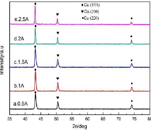
Fig.1 shows typical phases and microstructures of porous Cu foams electrodeposited at different cathodic current density in a 0.2M CuSO4 and 1.0 M H2SO4 solution. The crystal structure of porous films belongs to the face-centered cubic copper owing to the fact that most of the diffraction peaks observed are indexed to the Cu phase such as Cu (111), Cu (200) and Cu (220). In addition, it is obvious that there is no oxide of copper during the electrodeposition process although the porous copper is easy to be oxidized. The reason for this phenomenon is that the existence of abundant protons in the electrolyte leading to the highly acidic atmosphere, which not only effectively suppresses the oxide formation [7] but also accelerates the reduction of copper to metallic copper according to the following equations: CuO + 2H + →Cu2+ + H2O and Cu2O + 2H+ →Cu2+ + Cu + H2O.
[image:3.596.173.423.504.720.2]
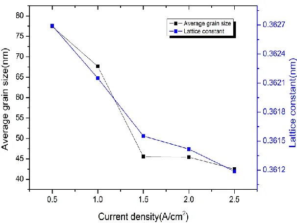
Comparing the XRD patterns obtained at different deposition current, it is found that the diffraction intensity of porous copper films is not sensitive to the current density. However, the grain size and lattice constant calculated according to the XRD patterns are closely related to electrodeposition conditions, especially current density. As shown in Fig2, the average grain size and lattice constant of copper all decrease at the current density of 0.5A/cm2 to 2.5A/cm2, which means the finest grain can be obtained at high current density, such as 2.5 A/cm2. This phenomenon can be explained through the following classical theory. The nucleation rate w induced by electrochemical deposition can be calculated by the following equation: 2
1exp 2
k
k
w k
, where k1、k2 is the
constant, is the over potentiality. The dependence of the critical nucleation radius on the over potentiality can be expressed as the following formula: 3
c
k πh E r
6Zeη
, where E is interfacial
energy, Z is the electron number of discharge ions, h is the height formed by absorbent atoms. According to the above equations, the nucleation rate increases and critical nucleation radius decreases with increasing the over potentiality and current density, which is beneficial to the formation and refinement of the initial grain. Meanwhile, the evolution rate of hydrogen bubbles gradually increases with increasing the current density, which produces much larger driving force for H2 bubbles to deviate from the cathode copper foil [17]. Consequently, the crystal growth time will be shortened, which also contributes to the refinement of porous copper grain.
Figure 2.The dependences of the average grain size and lattice constant on the current density
[image:4.596.177.480.425.653.2]
surface of cathode and different scattered agglomerates closely connect with each other in the pore walls.
[image:5.596.188.446.120.700.2]
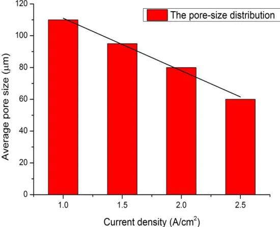
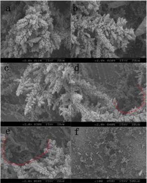
Further increasing the current density to the value of 1.5A/cm2, the mixture of intensive dendrites and corn-like agglomerates of copper grains are formed, as shown in the enclosed circle of Fig.3 (h, i). Meanwhile, the dendrites have a trend to grow towards the interior of pores resulting in a more close three-dimensional structure. Hence, increasing the current density properly could contribute to the formation of the three-dimensional structure of porous copper foams. According to the present research, the morphology of porous structure is mainly caused by the competitive reaction between hydrogen evolution and copper deposition [7]. Different dynamic template can be obtained by adjusting the current density, since the evolution rate of hydrogen bubbles is closely related to the deposition current. At low current density, few H2 bubbles can evolve from the surface of copper substrate, therefore, producing lots of available deposition areas on the cathode foil, making it difficult for Cu2+ to form interconnected porous structure. This is the reason why the scattered and irregular morphology of copper films appear on the surface of cathode. With increasing current density, abundant hydrogen bubbles formed and clustered, which inhibited the growth of copper towards the hydrogen bubbles, making the electrochemical reaction only occurs at the interstices of hydrogen bubbles. In other words, the hydrogen bubbles act as a dynamic template for copper deposition and the formation of the porous structure during the electrodeposition process[18]. As seen from Fig.3d and Fig.3e, all the deposits are porous foam structure, while there’re still some differences in their structure, such as wall width and surface pore size. The latter pore size is obviously smaller than the former due to the fact that the hydrogen evolution rate increases with increasing the current density, leading to the formation of smaller bubbles [17]. Fig.4 display the pore-size distribution of three-dimensionally copper porous films obtained at various deposition current densities. The average pore size ranges from 60μm to 110μm as the distribution diagram shown.
[image:6.596.174.449.471.694.2]
3.2 Influence of deposition temperature
Figure 5. The typical phase composition of the Cu foams obtained at various deposition temperatures
[image:7.596.209.425.108.292.2] [image:7.596.169.465.341.710.2]
Fig.5 shows the typical XRD patterns of the porous copper films obtained at different deposition temperatures. It is clear that the diffraction peak positionsare identical to the XRD patterns shown in Fig.1, indicating that the principal phase is still face-centered cubic copper and no impurity phase exists. In contrast to Fig.1, the diffraction peak intensity of the same crystal face gradually decreases with increasing the deposition temperature, which means the lattice structure is highly sensitive to the change of deposition temperature. One reasonable explanation is that the electrochemical reaction and diffusion rate of ions are accelerated with increasing the reaction temperature[19], as a consequence of this, there is not enough time to develop the crystal structure without defect. Meanwhile, it can be seen that the full width at half maximum (FWHM) decreased slightly with increasing bath temperature, indicating high temperature environment is of benefit to crystal coarsening because of faster growth of the formed nuclei in this condition[20]. Similarly, there is no impure phase in diffraction patterns due to the existence of acidic environment.
Fig.6 displays the higher magnification SEM images of the porous copper electrodeposited in the “standard bath” at the current density of 1.0 A/cm2
[image:8.596.151.487.391.633.2]and at different deposition temperatures (RT-60 ℃). Comparing the lower magnification morphologies shown in Fig.3, corn-like dendrites and hemispherical pores can be clearly observed in this field. From Fig.6, it is obvious that the bath temperature has a great influence on the morphology and microstructure of Cu foams, especially the pore size and dendrites feature.
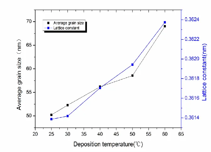
Figure 7. The dependences of the average grain size and lattice constant on the deposition temperature
hydrogen bubbles will become increasingly sparser. Therefore, the pore size of the porous copper films determined by the bubble sizes will increase.[22] This conclusion can be proved from the curvature of enclosed circles in Fig.4 (d, e). Meanwhile, high temperature provides more power for Cu2+ to deposit, which results in grain coarsening of the dendrites[21][23]. This change in morphology can be observed in the Fig.6 (a, e). Comparing various morphologies, it can be seen that rising reaction temperature plays a negative role in the copper grain refinement and the consistency of dendrites. In fact, the detrimental effect of deposition temperature became quite evident when the bath temperature is over 40 ℃. From Fig.6f, there is little interconnected spherical pore network on the surface of the copper substrate compared with the deposition morphology at RT.
The averaged grain sizes calculated in terms of Scherrer equation and lattice constant in porous copper foams obtained at different deposition temperatures are shown in Fig.7. There is an obvious positive correlation between the grain sizes and depositing temperature. It can be observed that with increasing deposition temperature, the average grain sizes increase from 50.23 nm (RT) to 69.04 nm (60 ℃), which is mainly caused by the high growth rate of grains at high depositing temperature [23]. Meanwhile, the partial deposition current density is subject to change with deposition temperature[21], which may also contribute to the grain enlargement. From the Fig.7, the lattice constant has similar change trend compared the average grain size and reaches a maximum value of 0.362374 nm at the temperature of 60 ℃. The increase of lattice parameter is due to the reason that with increasing the deposition temperature, copper atoms get more activation energy and diffusion speed can be accelerated obviously. Comparing with the PDF standard card, the relative increment of lattice constants can reach up to about 2%. The slight change of lattice constant implies the existence of lattice distortion, which is consistent with the dependence of diffraction peak intensity on temperature shown in Fig.5. Combining the above morphologies, it can be seen that rising temperature has a negative effect on the formation of integrated 3D porous structures and the regularity of the lattice.
4. CONCLUSIONS
the averaged grain sizes and deposition temperature. With increasing the depositing temperature, the average grain size increased from 50.23 nm (RT) to 69.04nm(60 ℃), indicating the existence of lattice distortion in the foams at high temperature.
ACKNOWLEDGEMENTS
This work was supported by the National Natural Science Foundation of China (Grant No 51071109) and the ‘Morning Star’ project of the Science and Technological Commission of Shanghai (Grant No 14QA1403600).
References
1. C. M. A. Parlett, K. Wilson, A. F. Lee, Chem. Soc. Rev.,42(2013)3876 2. L. Najdovski, P. R. Selvakannan, A. P. O’Mullane, RSC Adv., 4(2014)7207
3. E. Magoulianti, K. Beltsios, D. Davazoglou, N. Kanellopoulos, J. Phys. Chem. B, 11(2001)1191 4. J.-H Jeun, D.-H Kim, S.-H Hong , Sens. Actuators, B, 161 (2012) 784
5. X. Wang, B. Yang, K. Zhou, D. Zhang, Z. Li, C. Zhou, Curr. Appl Phys.,15(2015)662 6. F. Liang, Y. Yao, Y. Dai, B. Yang, W. Ma, T. Watanabe, Solid State Ionics, 214(2012)31 7. Y. Li, W.-Z Jia, Y.-Y Song, X.-H Xia, Chem. Mater., 19(2007)5758
8. N. D. Nikolic, G. Brankovic, M. G. Pavlovic, K. I. Popov, J. Electroanal. Chem., 621(2008)13 9. K. Tan, M. B. Tian, Q. Cai, Thin Solid Films, 518(2010)5159
10.D.H. Nam, R. H. Kim, D. W. Han, J.H. Kim, H. S. Kwon, Electrochim. Acta, 56(2011)9397 11.L. Xiong, Y.-X Huang, X.-W Liu, G.-P Sheng, W.-W Li, H.-Q Yu, Electrochim. Acta, 89(2013)24 12.I. Najdovski, P. R. Selvakannan, S. K. Bhargava, A. P. O’Mullane, Nanoscale, 4(2012)6208 13.H.C. Shin, M. Liu, Adv. Funct. Mater., 15 (2005) 582.
14.Y. Liu and S. Dillon, Chem. Commun., 50(2014)1761
15. H. Zhang, Y. Ye, R. Shen, C. Ru, Y. Hu, J. Electrochem. Soc.,160(2013)D441
16.Nikolic, D. Nebojsa, Brankovic, Goran, Maksimovic, M. Vesan, J. Solid State Electrochem., 16(2012)321
17.Y. H. Zhao, T. Masuoka, T. Tsuruta, Int. J. Heat Mass Transfer, 45(2002)3189
18.G. A. Lange, S. Eugenio, R. G. Duarte, T. M. Silva, M. J. Carmezim, M. F. Montemor, J. Electroanal. Chem.,737(2015)85
19.H. H. Abdel Rahman, A. H. E. Moustafa, S. M. K.Abdel Magid. Int. J. Electrochem. Sci.,7(2012)6959
20.R. Inguanta, F. Vergottini, G. Ferrara, S. Piazza, C. Sunseri, Electrochim. Acta,55(2010)8556 21.X. Qiao, H. Li, W. Zhao, D. Li, Electrochim. Acta,89(2013)771
22.B. J. Plowman, L. A. Jones, S. K. Bhargava, Chem. Commun.,51(2015)4331 23.W. Lu, P. Huang, C. He, B. Yan, Int. J. Electrochem. Sci., 7 (2012) 12262