Int. J. Electrochem. Sci., 8 (2013) 2430 - 2439
International Journal of
ELECTROCHEMICAL
SCIENCE
www.electrochemsci.org
Short Communication
Bi - Structure ZnO Prepared via Cathodic Electrodeposition
Method
N. H. Al-Hardan1,*, M.A. Abdul Hamid2, Azman Jalar1, Lim Karkeng2, R. Shamsudin2 and B.Y. Majlis1
1
Institute of Microengineering and Nanoelectronics (IMEN)
2
Faculty of Science & Technology, Universiti Kebangsaan Malaysia, 43600 Bangi, Selangor, Malaysia
*
E-mail: [email protected]
Received: 23 October 2012 / Accepted: 27 January 2013 / Published: 1 February 2013
This study addresses the producing of bi structure zinc oxide (ZnO) via chemical electrodeposition on a conductive coated glass. The current density was fixed at 2mA.cm-2 with different reaction time (deposit time). The produced ZnO shows a polycrystalline nature with prefer orientation towards the (a – axis). The reaction time shows no effect on the crystalline size and the microstrain, which proof the repeatability in the microstructural properties. The scanning electron microscopy (SEM) images show the presence of bi structures, the bottom is a submicron size plates, after that urchins like structure of ZnO were growth on the edge of the plates. More reaction time produced higher density of the urchins. The ZnO exhibit prominent emission at the UV band (3.27 eV) and no visible emissions were found. Blue (2.83 eV) and red luminescence bands (1.63 eV) were observed which was attributed to zinc interstitial to oxygen interstitial defect levels.
Keywords: Chemical – electrodeposition; Zinc oxide films; nano structures; photoluminescence spectra.
1. INTRODUCTION
varistors [9], gas sensors [10, 11], thin film transistors (TFT) [12] and as piezoelectric nanogenerators that can serve as self power sources for micro and nanosystems [13]. Comparing with many competitive compounds, ZnO can be prepared through simple methods with high quality. Methods such as sputtering [12], thermal oxidations [14], sol-gel [15], chemical vapor deposition [16] and chemical – electrodeposition [17, 18]. The chemical – electrodeposition method subject of increasing attention for producing ZnO, among the advantages is it considered a simple and low coast method [19]. The process use zinc chloride (ZnCl2) or zinc nitrate Zn(NO3)2 as a precursor [20]. The method
utilizes a low cathode voltage or current to produce the ZnO films at any conductive substrate such as glass coated with conductive layers or silicon wafers [18]. In the case of using constant cathode voltage, the force to the reaction will maintain constant whereby, the current constant source will maintain a constant reaction rate [20]. The method consists in generating hydroxide ions at the surface of an electrode by catholically reducing an oxygen precursor. The main oxygen source for this reaction is the dissolved molecular oxygen or nitrate ions [21]. The prepared films of the ZnO show different structures depending on parameters such as the salt concentrations, applied voltages, solution temperatures and substrates used [16, 22].
In spite of many published works deal with this process few were published showing the effect of the current density on the morphology and structure of the prepared ZnO films.
In this work, we report in the effect of different deposition periods on the structure and optical properties of the produced ZnO thin films using the chemical – electrodeposition.
2. EXPERIMENTAL DETAILS.
Bi-structure ZnO thin films were prepared via chemical – electrodeposition method on glass slides coated a conductive layer of indium tin oxide (ITO) with a sheet resistance of was approximately 20/ (BSJ Group - China). The substrates were cut in 1.0 x 1.5 cm, and then cleaned in acetone, ethanol and water in an ultrasonic bath for 15 minutes each. The electrolyte was an aqueous solution of zinc chloride (ZnCl2) act as Zn source, and potassium chloride (KCl) both are reagent grade
from Merck. The aqueous solution was prepared using 15 mM concentration of ZnCl2 0.1 M
concentration of KCl and was dissolved in 100 ml deionized water (resistance ~ 18 M). The KCl was used to ensure a good conductivity in the aqueous solution. Two electrodes cell were used to produce the ZnO. The ITO glass was used as a working electrode, and a high purity platinum wire (Pt) with a diameter of 0.5 mm was used as a counter electrode. The current density was fixed at 2 mA.cm-2 with reference to the Pt; the electrolyte was maintained at 80 oC. The temperature of C using a bath water, and was continuously stirred using a magnetic stirrer. During the electrodeposition, atmospheric air (as oxygen source) was bubbled (with low flow rate) through the solution near the ITO substrate in order to maintain a relatively high level of oxygen dissolved in the solution [23].
The dissolved oxygen is essential for the oxide growth (ZnO), once the negative potential is applied to the working electrode the reaction will start. The deposition reaction in the electrolyte is as follows [19]:
2
2
1
2 (1) 2
The deposition time was changed in 5 minutes interval from 5 to 20 minutes with constant current density. The current was sourced using the Agilent E3631A power supply. The produced samples were carefully rinsed with deionized water to remove chloride salts and then were dried in a hot plate at 80 oC for 15 minutes. The prepared films were annealed at a temperature of 500 oC for 1 hr in ambient atmospheric condition using a controllable tube furnace.
The surface morphology and the structure of the ZnO films were investigated using scanning electron microscopy (SEM), LEO 1450VP from Zeiss and for the structure determination X-ray diffraction (XRD), D8 ADVANCE from BRUKER using a copper (Cu) target that emits X- ray with a wavelength of 0.154 nm. The operating voltage of the XRD was fixed at 60 KV and the current at 60 mA. For the optical measurements, the photoluminescence (PL) spectra were recorded using the FLS920 supplied by Edinburgh photonics. The measurement range was from 320 to 800 nm using a xenon lamp (450 W) and the excitation wavelength at 300 nm. All the measurements were taken at atmospheric environment (temperature 21 and humidity 50%).
3. RESULTS AND DISCUSSIONS
3.1. The Structure and morphology of the produced films
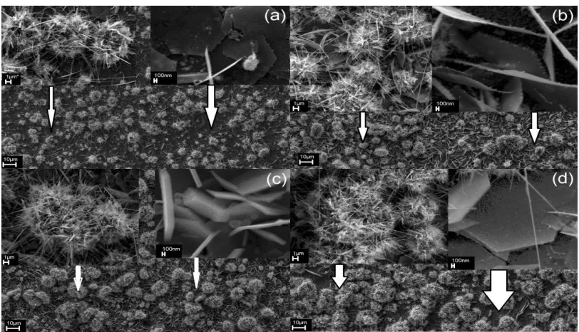
[image:3.596.100.506.453.686.2]The SEM images of the produced ZnO at different deposition time are depicts in Fig (1 (a), (b), (c) and (d)) which correspond to the deposition time of 5, 10, 15 and 20 minutes respectively. The image clearly shows two different structures on the same substrate.
Both structures are repeated with different deposition time. The images show the increased in the density of the structures as can be seen in the lower portion of the images in Fig. 1. The two structures found are the 2D plates (the upper right hand side of each image in Fig.1). This structure was reported early by several groups using glass coated by transparent conductive layers [24, 25]. The other structures have the urchin like structures. These urchins are grown on spots (the bright spots as can be seen from the upper right hand side of each image in Fig.1) at the plate’s edges. The images also show the bridging between the nanowires of the ZnO, which it is believed to be the last stage of the growth. More reaction time will result in the agglomeration of the urchin structures, and then the growth of the extended nanowire of the ZnO as it can be seen in the upper right hand side of Fig 1(d). It is believed that the decrease of the potential field as thicker became the ZnO layer may be the reason of such phenomena.
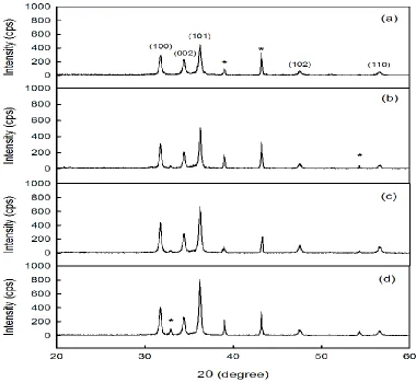
Fig (2) depicts the XRD pattern of the prepared ZnO films at different time. The diffraction peaks related to ITO-coated glass is indicated by ∗ (star). The pattern proves the polycrystalline nature of the produced ZnO. According to JCPDS 036-1451 card, the resulting patterns matched well with the hexagonal (Wurtizite) crystal structure of the ZnO.
[image:4.596.101.481.338.687.2]
The intensity of the ZnO phases increased gradually via the increasing in the reaction time of chemical electrodeposition process, and as consequence the agglomeration of the ZnO structures increased (the density of the ZnO structure as can be seen from the SEM images).
Preferential orientation of the ZnO can be estimated by calculating the texture coefficients (TC) using [26]:
( ) / ( )
( ) (2) (1/ ) ( ) / ( )
o oI hkl I hkl TC hkl
n I hkl I hkl
where I(hkl) are the measured XRD relative intensity of a plane (hkl), Io(hkl) is the standard
[image:5.596.112.480.377.640.2]intensity of the plane (hkl) taken from (JCPDS 036-1451 card) and (n) is the number of diffraction peaks considered. According to Eq. 2, the ZnO films will present preferential orientation if the TC for a specific (hkl) plane is greater than unity. The TC for the three main ZnO reflections (100), (002), and (101) present in the XRD patterns of the produced ZnO films, those reflections were chosen as they indicate the change in the crystal form. The TC results are shown in Table 1.
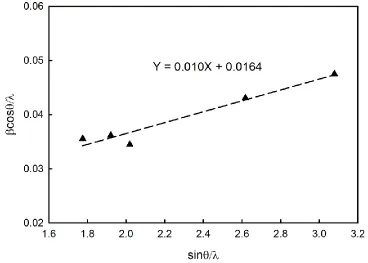
Figure 3. The W-H plot of the produced ZnO at deposition time of 20 min on ITO substrate.
X-ray profile analysis is a powerful tool to study the microstructural of the thin films using the boarding in the peak. The micro strain ( ) and crystallite size (D) can be calculated using Williamson– Hall (W–H) plot with following relation [26, 27].
cos 1 sin
(3)
D
where and represent the Cu wavelength (0.154 nm), the full-width at half-maximum (FWHM) and the Bragg angle respectively. From Eq. (3) it is clear that by plotting cos
against
sin
we get a straight line with the intercept on the Y axis reveals the particle size corresponding to zero strain and the strain e is determined from the slope of the line. Fig 3 depicts this plot for the 20 minutes deposition time. The results of both D and of the other samples deposited at different time are tabulated in Table 1.
Table 1. The texture coefficients TC (hkl), crystallite sizes (D) and the strain (e) of the produced ZnO films at different time.
Deposition TC (khl) D (nm) ε Time (min) (100) (002) (101)
5 0.633 1.071 1.296 50 0.016
10 0.6 1.035 1.365 41 0.007
15 0.66 0.959 1.381 41 0.008
20 0.622 0.895 1.483 60 0.01
From the tabulated results, it is obvious that the increasing in depositing time has an insignificant effect on both crystallite size and the strain. This mean that the produced ZnO under the constant current show repeatability in it microstructural properties.
3.2. Emission properties
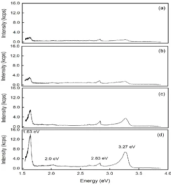
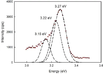
The room temperature PL spectrum under the excited wavelength of 300 nm of the prepared ZnO thin films on ITO glass substrates are shown in Fig 4 (a), (b), (c) and (d). The wavelength range was from 320 to 800 nm (3.87– 1.55 eV). The spectrums show the dominant UV emission peak at around 3.27 ± 0.02 eV (379 nm) for all the prepared samples. The Y-axis of the graphs was kept constant for comparison purpose.
clear that it consist of several emissions at the shoulder of the low - energy side. Fig.5, depicts the UV peak of the produced ZnO, and it is clear that there are two extra peaks located at 3.22 and 3.15 eV which they can be identify as the longitudinal-optical (LO) phonon of the D0 X emission with a difference of 72 meV each [28].
Noteworthy, that there was no clear visible emission (green – yellow around 2.25 eV) in all the produced samples. This implies the limited existence of oxygen vacancies in the prepared ZnO [28]. Instead, the emission band at 2.83 eV (blue) was observed. This band is attributed to the oxygen vacancies or to the zinc interstitials [29, 30].
[image:7.596.121.473.248.629.2]
Figure 5. The UV emission of the produced ZnO at deposition time of 20 min. The dashed lines represent the Gaussian fitting of the emissions.
In the case of this study it is believed that the origin of this band is the zinc interstitials as the absence of the green-yellow band proves that the oxygen vacancies are limited.
Furthermore, the electroluminescence measurements of pure ZnO [29] attributes the origin of this emission to the recombination between the zinc interstitials energy level to the zinc vacancies energy level with energy approximately 2.84 eV. The result of this transition in consistent with the photon energy of the blue emission observed in this study (2.83 eV).
[image:8.596.121.476.86.341.2]
4. CONCLUSION
ZnO bi structures were growth using chemical electrodeposition on ITO glass. The current density was fixed at 2 mA. cm-2, and the reaction time (deposition time) was changed in the interval of 5 minutes up to 20 minutes. The XRD pattern of the produced layers has a polycrystalline nature. Furthermore, the SEM images depict the bi structures of the ZnO one has the plate shape while the other has a urchin like structure. Distinguish photon emissions were absorbed, the first was at the UV band, and the second was at the NIR band, both show a significant enhanced with the reaction time.
ACKNOWLEDGEMENT
This work was supported by the Universiti Kebangsaan Malaysia (UKM) through the short-term grants (OUP-2012-120) and (DIP -2012-2014). The authors are also thankful to the Centre for Research and Instrumentation Management (CRIM) - UKM for providing the PL measurements and VPSEM.
References
1. H. Morkoç, Ü. Özgür, Zinc Oxide: Fundamentals, Materials and Device Technology, Wiley-VCH, 2009.
2. U. Ozgur, Y.I. Alivov, C. Liu, A. Teke, M.A. Reshchikov, S. Dogan, V. Avrutin, S.J. Cho, H. Morkoc, J. Appl. Phys. , 98 (2005) 041301-041103.
3. W. Zhong Lin, J. Phys.-Condes. Matter 16 (2004) R829.
4. J. Zhong, Y. Lu, ZnO-Based Ultraviolet Detectors, in: C.W. Litton, T.C. Collins, D.C. Reynolds, P. Capper, S. Kasap, A. Willoughby (Eds.) Zinc Oxide Materials for Electronic and Optoelectronic Device Applications, John Wiley & Sons, 2011.
5. M.H. Huang, S. Mao, H. Feick, H. Yan, Y. Wu, H. Kind, E. Weber, R. Russo, P. Yang, Science, 292 (2001) 1897-1899.
6. C. Jagadish, S. Pearton, Zinc Oxide Bulk, Thin Films and Nanostructures Processing, Properties and Applications, ELSEVIER, 2006.
7. C.W. Litton, T.C. Collins, D.C. Reynolds, P. Capper, S. Kasap, A. Willoughby, Zinc Oxide Materials for Electronic and Optoelectronic Device Applications, John Wiley & Sons, 2011. 8. Ecospark, ZnO nanowire LED-chip, in, Ecospark, http://ecospark.se/products/product-1, access
date was 2012.
9. G.D. Mahan, L.M. Levinson, H.R. Philipp, J. Appl. Phys., 50 (1979) 2799-2812. 10.O. Lupan, G. Chai, L. Chow, Microelectron. Eng., 85 (2008) 2220-2225.
11.N. Al-Hardan, M.J. Abdullah, A. Abdul Aziz, H. Ahmad, Appl. Surf. Sci. , 256 (2010) 3468-3471. 12.P.F. Carcia, R.S. McLean, M.H. Reilly, J.G. Nunes, Appl. Phys. Lett., 82 (2003) 1117-1119. 13.Z.L. Wang, MRS Bulletin, 37 (2012) 814-827.
14.N. Al-Hardan, M.J. Abdullah, A.A. Aziz, Appl. Surf. Sci. , 255 (2009) 7794-7797. 15.J.-H. Lee, K.-H. Ko, B.-O. Park, J. Crystal Growth, 247 (2003) 119-125.
16.L.N. Protasova, E.V. Rebrov, K.L. Choy, S.Y. Pung, V. Engels, M. Cabaj, A.E.H. Wheatley, J.C. Schouten, Catalysis Science & Technology, 1 (2011) 768-777.
17.T. Yoshida, D. Komatsu, N. Shimokawa, H. Minoura, Thin Solid Films, 451–452 (2004) 166-169. 18.L. Yu, G. Zhang, S. Li, Z. Xi, D. Guo, J. Crystal Growth, 299 (2007) 184-188.
19.T. Pauporté, D. Lincot, Electrochim. Acta, 45 (2000) 3345-3353. 20.S. Xu, Z. Wang, Nano Res., 4 (2011) 1013-1098.
22. . Mar , M. Mollar, A. Mechkour, B. Hartiti, M. Perales, J. Cembrero, Microelectron. J., 35 (2004) 79-82.
23.N.H. Al-Hardan, M.J. Abdullah, N.M. Ahmed, F.K. Yam, A. Abdul Aziz, Superlattices and Microstructures, 51 (2012) 765-771.
24.F. Wang, R. Liu, A. Pan, L. Cao, K. Cheng, B. Xue, G. Wang, Q. Meng, J. Li, Q. Li, Y. Wang, T. Wang, B. Zou, Mater. Lett., 61 (2007) 2000-2003.
25.H. Kim, J.Y. Moon, H.S. Lee, Electronic Materials Letters, 5 (2009) 135-138.
26.M. Birkholz, Thin Film Analysis by X-Ray Scattering, WILEY-VCH Verlag GmbH, 2006. 27.S.K. Mishra, R.K. Srivastava, S.G. Prakash, J. Alloys and Compounds 539 (2012) 1–6.
28.S. Y lmaz, M. Parlak, Ş. Özcan, M. Altunbaş, E. McGlynn, E. acaks z, App. Surf. Sci., 257 (2011) 9293-9298.
29.N.H. Alvi, K.u. Hasan, O. Nur, M. Willander, Nanoscale Research Letters, 6 (2011) 130. 30.D.H. Zhang, Z.Y. Xue, Q.P. Wang, J. Physics D: Applied Physics, 35 (2002) 2837. 31.Aleksandra B. Djuriscaroni, cacute, Y.H. Leung, Small, 2 (2006) 944-961.