Abstract: The modular inversion operation is an essential hardware design for computing speed when we use it in cryptography applications. Through this work, we present a FSM based design methodology to achieve speed, area and high-performance modular binary inversion algorithm over 256-bit prime field. The proposed architecture implemented using Xilinx Virtex-7 FPGA device, it achieves 37% reduction in area-delay product and 15% and 16% of improvement in speed and throughput respectively, when compared with existing designs. Also, ASIC based implementation is done using TSMC 65nm CMOS technology, the synthesis results achieved the maximum operating clock frequency is 833 MHz and throughput of 626Mbps, which makes it suitable for speed-critical crypto- applications.
Index Terms: Modular inversion, Field-programmable gate-array (FPGA), Elliptic curve cryptography (ECC), Application specific integrated chip (ASIC).
I. INTRODUCTION
Cryptography aims to hide the information message through a public communication channel, which applies principles of mathematical algorithms. These algorithms extensively involve modular arithmetic operations in a large Galois Fields. Such operations are modular inversion, multiplication, subtraction and addition. In recent years, elliptic curve cryptography (ECC) has been adopted by growing Internet of Things (IoT) based applications in industries, that work on innovative security technologies. The modular inversion is one of the essential operations required by cryptographic algorithms or this operation cannot be avoided in practical cryptographic applications and also it is time consuming operation. It is important to ensure that the modular inversion logic is implemented to achieve optimized area and performance while using in affine coordinate systems. FPGA technology has a greater flexibility to implement cryptographic algorithms.
The goal is to implement high speed modular binary inversion algorithm over 256-bit prime field using architectural optimization techniques and algorithmic reformulations for ECC using FPGA / ASIC-based design technology. This paper is organized as follows: literature review is presented in section. II. A brief mathematical background about ECC and modular inversion is described in Section. III. Register-Transfer Logic (RTL) model for inversion algorithm implementation or Finite-state machine
Revised Manuscript Received on July 05, 2019.
Thirumalesu Kudithi, School of Electronics Engineering, Vellore Institute of Technology, Vellore-632014, India.
Sakthivel R, School of Electronics Engineering, Vellore Institute of Technology, Vellore-632014, India.
with data-path (FSMD) for modular inversion and its components presented in Section. IV. The improved results achieved through FPGA and ASIC implementation in comparison with other available designs shown in Section. V. The final section concludes the paper by summarizing the advantages of the proposed architecture.
II. LITERATURESURVEY
In literature, three well-known methods that are used to compute modular inversion/division: Extended Euclidean Algorithm (EEA), Montgomery modular inversion method and Fermat's Little Theorem (FLT). One of the efficient algorithm Binary Inversion Algorithm to compute modular inversion, which is easier to implement RTL based hardware perspective and also more area-efficient with high-speed operation. The modular inversion/division algorithm for ECC
over
F
pwas developed by Hossain [1, 2], Javeed [3]–[4],Mrabet [5], Kudithi [6], Liu [7], Lee [8], Vliegen [9], Ghosh [10], McIvor [11], and Daly [12-13]. Among these McIvor described different hardware architectures for modular inversion algorithm and remaining authors are used binary inversion algorithm or extended Euclidean algorithm. To implement hardware, Xilinx platform with Virtex-7 FPGA is used.
III. BACKGROUND A.Definition of elliptic curve
The simplified Weierstrass elliptic curve E is given in form:
b
ax
x
y
E
:
2
3
(1)Above equation exists in prime field
F
p(
p
3
)
,constant curve parameters are
a
andb
. The pointsrepresented in curve using affine coordinates are
(
x
,
y
)
.Equation (1) satisfies cyclic abelian group operations over
prime field,
F
p and it need to satisfy sufficient condition.
0
27
4
a
2
b
3
Let
P
(
x
1,
y
1)
andQ
(
x
2,
y
2)
are two points representedon curve, then the group operation of point addition operation
gives another point
R
(
x
3,
y
3)
on curve, i.e.,)
(
R
P
Q
would be calculated as follows.An Efficient Hardware Implementation of Finite
Field Inversion for Elliptic Curve Cryptography
)
/(
)
(
;
)
(
;
1 2 1 2 1 3 1 3 2 1 2 3x
x
y
y
where
y
x
x
y
x
x
x
(2)The other group operation, point doubling operation
defines adding a point on curve
P
(
x
1,
y
1)
to itself giveanother point
R
(
x
3,
y
3)
on curve, i.e.,R
2
P
(
P
P
).
It would be calculated as follows.
1 2 1 1 3 1 3 1 2 3 2 / ) 3 ( ; ) ( ; 2 y a x where y x x y x x
(3)The equations (2) and (3) requires modular arithmetic operations like inversion/division, multiplication, subtraction and addition. The hardware design for division or modular inversion necessary required in affine coordinates to calculate the slope of the curve
value.In ECC system application, EC-Scalar Multiplication (ECSM) is a necessary computing operation which requires repeated point addition and point doubling operations. So, when we prefer affine coordinates, modular inversion has to be computed many times as compared to projective coordinates. The methodology to represent various projective points and point operations are described in detail in elliptic curve cryptography [14]. Using projective coordinates helps in replacing computational cost intensive field inversion by less expensive field multiplication. These arithmetic operations are done in different projective coordinates systems. So, the ECSM using projective coordinated still requires at least one modular inversion operation. This security is depends upon the discrete logarithm with respect to a given base point input. Moreover, this inversion algorithm is useful in Miller algorithm to compute ECSM in pairing based cryptography.
B.Modular inversion
In ECSM, very expensive and time consuming operation is modular inversion, which is required to perform point addition and point doubling operations. However, one inversion operation is still required in projective coordinate and mandatory in affine coordinates. This operation performs in finite field of order is
p
with modulo prime],
1
,
0
[
n
p
wheren
log
2P
is the bit length ofp
. Inother words the range of
p
value is2
n1
p
2
n. Thisfinite field operation denotes by
F
p. The division operationrepresents
(
b
/
a
)
mod
p
,
for any inputsa
,
b
andp
, to findthe reminder is called reduction modulo, denotes
q
,
where
q
[
0
,
n
1
].
The classical definition for multiplicative inverse or
modular inversion over prime field
F
pcan be obtained byforcing input . This operation can be represented as
)
(mod
1
.
)
(
mod
1p
R
a
or
p
a
R
(4)Where
a
an integer and the prime isp
with maximum lengthof bit
n
. This inverse existsa
andp
must be relativelyprime. Moreover the computation of division or inversion takes the same amount. An example of a modular inverter: Let
a
13
and modulusp
17
then
]
1
)
17
,
4
(
1
17
mod
13
*
4
[
4
17
mod
13
mod
1 1
GCD
or
because
p
a
R
The modular inversion/division can be computed in several ways based on the architecture used with the size and type of the field over a finite field,
F
p [15]–[16]. The following arethe list of algorithms used for computing modular inversion.
Fermat's little theorem,
Dimitrov-Järvinen (DJ) method,
Montgomery multiplication method,
Extended Euclidean algorithm,
Itoh-Tsujii multiplicative inverse algorithm,
Almost Inverse Algorithm,
Kaliski's Montgomery inversion algorithm.
Among these algorithms, the Extended Euclidean Algorithm or Binary Euclidean Algorithm is efficient way and simple to compute modular inversion. The other method is the Ferment’s little theorem is useful to create constant time modularity to avoid attack in ECC like power attacks.
C.Introduction to high level state machine model
Most of the designers starts with C-code and can be implemented in HLSM (high level state machine). This HLSM is used to describe FSMD (finite state machine with data-path). The basic information of FSMD based has been provided in the book [17]–[19]. To convert any algorithm to RTL, Some rules need to be followed while converting to HLSM from basic types of C-code, the templates of which are shown in Fig. 1. It consists different basic constructs of C-code to translate into HLSM states representation, this process are mostly self-explanatory [19].
IV. HARDWARE DESIGN FOR INVERTER OVERFp
This section presents FSM based hardware architecture implementations for modular inversion algorithm. The National Institute of Standards and Technology (NIST)
standard chosen for elliptic curves over
F
256to implementmodular inversion algorithm [20]–[21].
Algorithm 1 is a well-known method to compute modular inversion over the prime field. This is used four intermediate variables, i.e.,
u
,
v
,
x
andy
. The even or odd numbersrepresented by the single bit variables
u
0andv
0 and which istarget = expression target = expression
if (cond) { //then stmts }
! cond
cond
(then stmts)
while (cond) {
//while stmts }
! cond
cond
(while stmts)
for (i=0 to n-1) { //for loop stmts
} (i < n)
(for stmts) i=0
! (
i <
n
)
(end) (end)
if (cond) { //then stmts }
else {
//then stmts }
! cond
cond
(then stmts) (else stmts)
(end) (a)
(b)
(c)
(d)
(e)
Fig.1 Template structure: (a) assignment statements (b) if-then statements (c) if-then-else statements (d) while loop
statements (e) for loop statements
The hardware architecture of inversion algorithm works iteratively and it consists a series of additions/subtractions, and shift operations. At least one bit length is reduced either
u
orv
variable at each loop iteration. The result of modular inversion represented R over prime fieldF
p.In FSM method, the approach to design HLSM for modular inversion algorithm is described. The basic C-language to HLSM template or FSM based constructs are discussed in section III.C [17]–[19]. These constructs help in easily implementing RTL based architecture and enables us to generate HDL code for any algorithm. By using this constructs, we translated into basic HLSM for Algorithm 1 as shown in Fig. 2.
Algorithm 1 Binary inversion algorithm over Fp [1, 10]
Input: prime
p
anda
[
p
1
]
Output:
R
a
1mod
p
1:
u
a
;
v
p
;
x
1
;
y
0
2: whileu
1
;
v
1
do3: while
u
is even do uu/2 3.1: ifx
is even xx/2 3.2: elsex
(
x
p
)
/
2
;
end if 3.3: end while4: while
v
is even dov
v
/
2
4.1: ify
is eveny
y
/
2
42: else
y
(
y
p
)
/
2
;
end if 4.3: end while5: if
u
v
thenu
u
v
5.1: if
x
y
thenx
x
y
5.2: else
x
(
x
p
)
y
; end if 5.3: elsev
v
u
5.4: if
y
x
theny
y
x
5.5: else
y
(
y
p
)
x
; end if 5.6: end if6: end while
7: if
u
1
thenR
x
mod
p
8: else if v1then
R
y
mod
p
; end if 9: Return (R)S0
S1
S2
S20
S21
S22
S3 S
8
rst
! Go
Go
u == 1
u == 1
v = = 1 u != 1
v = v / 2
y0 == 0
y = (y+p) / 2 ux
vy
u ≥ v ! (u ≥ v)
u = u-v v = v-u
x = x-y x = x+p-y y = y-x y = y+p-x
x > y y > x
R = x mod P
R = y mod P
! (x > y) ! (y > x)
S4
S5 S6
S7 x = x / 2
x0 == 0
x = (x+p) / 2
S9
S10 S11
S12 u = u / 2
! (x0 == 0) ! (y
0 == 0)
S13
S14
S15 S16
S17
S18 S19
v = v / 2
u0 == 0 v
0 == 0
! (u0 == 0) ! (v
0 == 0)
Load u, v, x, y
PSM
sig_inv = 1
sig_inv = 0 sig_inv = 0
This FSM consists of “states” and “arcs (arrows)” each state represents either an operational statement (i.e., arithmetic or shift operations) or null operation and each arc represents a conditional statement or passing of a signal value.
Fig. 2, consists of total 23 states and after synthesizing this FSM using synopsys tool, it might be reduces upto 10 states. The “Go” signal indicates the start of modular inversion process. The result R in state S21 or S22, requires one modulo
reduction operation. The modulo reduction hardware can be implemented using modular addition by tying one input to zero [12].
The FSM method, the implementation of inversion hardware requires four essential intermediate registers
x
v
u
,
,
andy
and needs to be initializedto
u
a
;
v
p
;
x
1
andy
0
along with the controlsignal “sig_inv” assigned to 0 in state S2. The LSB bits of
these intermediate registers are indicated by variables
0 0 0
,
v
,
x
u
andy
0.These intermediate register values will change while the state transitions from state S3 to state S19, and it repeats until
the condition
u
1
orv
1
becomes true. In state S20the control signal “sig_inv” is assigned to 1 and moves to next state S21 or S22 to compute the modular reduction operation,
which gets the result R, and assigns the control signal “sig_inv” to zero. Finally from state S21 or S22 FSM moves to
the initial state S0 to perform modular inversion for another set
of input values
a
andp
. The name of the dashed block ‘PSM’ indicates parallel state machine, the values of uxandx
v are computed in parallel when the condition u1 is
satisfied in state S2. When coding RTL for PSM block, using
the same variables
u
,
v
,
x
andy
for parallel computation instates S3 and S8 might cause a problem during synthesis. This
can be avoided by taking different register variables for computation in states S3 and S8. Which might impact the area
in ASIC implementation, but not in FPGA implementation. All intermediate signals or variables are bounded by
)
2
(
n
-bits throughout the calculation.The computation time for one modular inversion using FSM based implementation (proposed method), takes maximum
2
n
1
clock cycles (CCs) or an average10
33
.
1
n
CCs; wheren
is maximum length of bitsp
anda
[1-2].V.RESULTS AND PERFORMANCE ANALYSIS
This section presents the performance analysis of modular inversion over Fp, where prime p is 256-bits with our
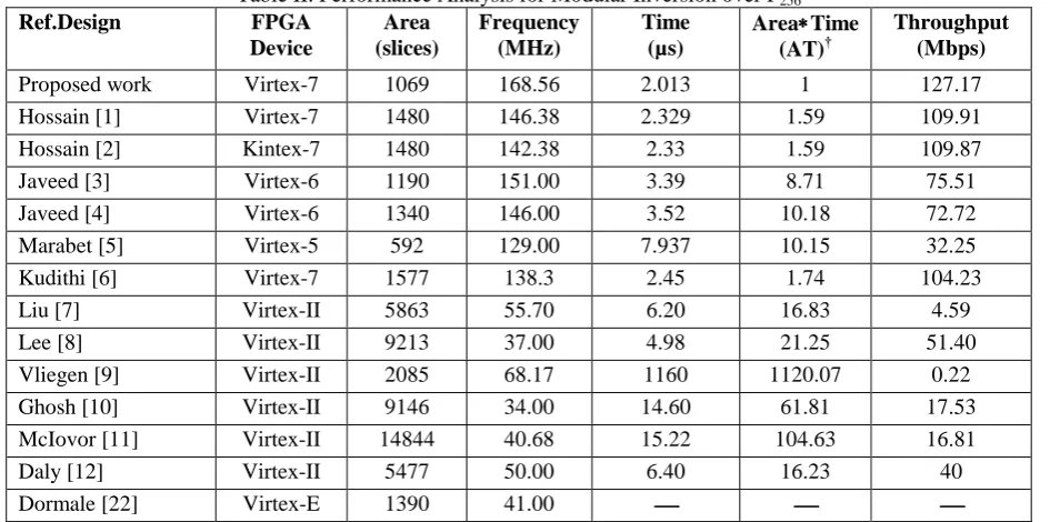
proposed architecture and existing designs using FPGA and ASIC. In our experiment, the modern 28nm Xilinx ISE 14.7 tools, Virtex-7 FPGA with Verilog HDL and device part number XC7V485T-2FFG1761 is selected to implement the modular inverter for synthesis and simulation, as it is advanced when compared with the Vertex II FPGA, which has been used in most of the available literatures. So, at present the Vertex II FPGA device is obsolete now. We have also compared our results with the available literature on design.
This design provides low hardware resources (low area) but the computation time is more. The performance metrics of AT is decreased around 90% and throughput is increased around 294%. So, our design provide better results in terms of AT and throughput with respect to recent designs are Hossain et al. [2], Javeed [3]–[4] and Mrabet et al. [5].
Our proposed methods for implementing the modular inverter achieves a computation time and frequency of 2.013µs and 168.56MHz respectively using Xilinx Virtex-7 FPGA over F256. Our proposed design provides 15%
improved frequency of operation as compared with previous designs [1]–[2]. The proposed method uses 1069 slices without DSP slices. We observed an area improvement of around 38% when compared with previous designs [1-2, 9]. The comparison of our results with available designs is not straight forward as most of the listed authors have implemented using different FPGA technology except Hossain et al. [1]–[2] and Kudithi et al. [9].
Table I, gives the summary of device utilization in FPGA. The major comparison is utilization of area and it is defined the total number of slices utilized in FPGA. The occupied area is 27.8% improvement using our FSM method when compared with [1]–[2], [9].
Most of the authors presented the hardware implementation for modular inversion using different FPGA platforms which makes the comparison is difficult. So, we used throughput rate parameter and area-delay product (AT) parameter for comparison purposes.
Table II, gives the simulated results and performance from various papers presented by Hossain et al. [2], Liu et al. [3], Lee et al. [4], Vliegen [5], Ghosh et al. [6], McIvor et al. [7], Daly et al. [8] and Kudithi et al. [9]. We can observe that the results from Hossain et al. [2] and Kudithi [9] are better in terms of area and computation time when compared with other literature results. Our proposed design gives even better results in terms of frequency of operation, computation time, AT and area when compared with reference designs [2] & [9].
Javeed [3]–[4] designs has implemented using Virtex-6 FPGA. The throughput is improved around 68% to 75% and AT is decreased around 88% to 90% when compared with our design. Mrabet et al. [5] design provides
4
n
clock cycles todevelop the modular inversion, where
n
log
2p and their design is used implementation hardware in Virtex-5 FPGA.Table I. Device utilization summary for inversion algorithm Numbers of
Logic Utilization
Proposed Design
Ref. [1]
Slice Registers 1310 1551
Slice LUTs 4035 5868
Fully Used LUT-FF Pairs 960 1291
BUFG/BUFGCTRLs 1 1
Bounded IOBs 516 516
No. of Occupied Slices 1069 1480
Table II. Performance Analysis for Modular Inversion over F256
Ref.Design FPGA
Device
Area (slices)
Frequency (MHz)
Time (µs)
AreaTime (AT)†
Throughput (Mbps)
Proposed work Virtex-7 1069 168.56 2.013 1 127.17
Hossain [1] Virtex-7 1480 146.38 2.329 1.59 109.91
Hossain [2] Kintex-7 1480 142.38 2.33 1.59 109.87
Javeed [3] Virtex-6 1190 151.00 3.39 8.71 75.51
Javeed [4] Virtex-6 1340 146.00 3.52 10.18 72.72
Marabet [5] Virtex-5 592 129.00 7.937 10.15 32.25
Kudithi [6] Virtex-7 1577 138.3 2.45 1.74 104.23
Liu [7] Virtex-II 5863 55.70 6.20 16.83 4.59
Lee [8] Virtex-II 9213 37.00 4.98 21.25 51.40
Vliegen [9] Virtex-II 2085 68.17 1160 1120.07 0.22
Ghosh [10] Virtex-II 9146 34.00 14.60 61.81 17.53
McIovor [11] Virtex-II 14844 40.68 15.22 104.63 16.81
Daly [12] Virtex-II 5477 50.00 6.40 16.23 40
Dormale [22] Virtex-E 1390 41.00
† Normalized value, AT = 1/0.00215932655 = 463.10735, where A: area (slices) and T: time (s).
Table III. ASIC Implementation with different case analysis Mode
Analysis
Field (bits)
Area (µm2)
Estimated Gate count
Frequency (MHz)
Power (mW)
Typical case F224
F256
63135.6 72027.2
28140
32109 833.33
17.12 19.54
Best case F224
F256
63827.2 71651.2
28572
31874 833.33
26.91 30.76
Worst case F224
F256
70449.6 79430.4
32828
36741 833.33
13.32 16.27
Moreover, Kudithi [6] design has decreased in the throughput of 22% when compared with our FSM method. The development of modular inversion in Virtex-II and Virtex-E are listed out and these designs are obsolete now. So we listed out those design values and estimated parameters but not compared with our designs.
Fig. 3 and Fig. 4 shows that the performance analysis of area-delay product and throughput measures with our design and existing designs. Among these the AT and throughput values of Ref. [1]–[2] and [6] are approximately equal with our design.
The design is also synthesized using Synopsys Design Compiler with Taiwan Semiconductor Manufacturing Company (TSMC) standard logic-cell library (65nm, 1.1V, 25oC). We are calculated power-delay product, area-delay product and throughput with estimated gate-count.
Table III shows various computed parameters used. The “area” is measured in (µm2), which is a total number of
2-input NAND gate equivalent; the “time” is the total computation time, “power” indicates the total power, which is a combination of internal power, switching power and leakage power values, the “energy” is a product of power and delay (Time), the ‘throughput’ is a measure of bit field over the computation time; these factors are calculated for design to finish one operation.
The proposed design methods is proven to be very fast, a frequency of 833.33 MHz with an optimal area of 72.0272
mm2 (32.109 K gates) and throughput rate of our design is 626 Mbps for modular inverter over F256. Table III gives the
result of three different (Typical case, Best case and Worst case) analysis, obtained from synthesis tool for proposed design over prime field F224 and F256.
In our proposed design method requires an average of
n
33
.
1
clock cycles (CCs) with an extra 10CCs to get proper output, because of the pipelining mechanism, it is sufficient to execute Algorithm 1.VI. CONCLUSION
This paper targeted to ECC applications and presented clearly the hardware architecture implementation for modular inversion over F256. The FSM based binary inversion
algorithm results for getting high speed nd low area on FPGA device compared to earlier designs. Our design method has achieved a maximum frequency of 168 MHz and throughput of 127 Mbps with the occupied area of 1069 slices. Synthesis results from Synopsys Design Compiler shows that, a maximum frequency of 833 MHz and throughput of 626 Mbps with consuming area of 32.1 K gates. These results makes our proposed designs more suitable for speed-critical cryptographic applications in
[image:5.595.110.486.346.445.2]of operation making it best suitable for ECC applications.
Fig.3 Comparison of our design AT with existing designs.
Fig.4 Comparison of our design throughput with existing designs.
ACKNOWLEDGMENT
The authors thank VIT for providing ‘VIT SEED GRANT’ for carrying out this research work.
REFERENCES
1. M. S. Hossain, and Y. Kong, “High-performance FPGA implementation of modular inversion over F256 for elliptic curve
cryptography”, in IEEE International Conf. onData Science and Data Intensive Sys. (DSDIS), IEEE, 2015, pp. 169-174, 2015.
2. M. S. Hossain, Y. Kong, E. Saeedi, and N. C. Vayalil, “High-performance elliptic curve cryptography processor over NIST prime fields”, IET Comput & Digital Tech., Vol.11, No.1, pp.33-42, 2016.
3. K. Javeed, and X. Wang, “Low latency flexible fpga implementation of point multiplication on elliptic curves over GF (p)”, International Jour of Circuit Theory and Appl., Vol. 45, No.2, pp.214-228, 2017. 4. K. Javeed, X. Wang, and M. Scott, “High performance hardware
support for elliptic curve cryptography over general prime field”,
Microprocessors and Microsystems Vol.51, pp.331-342, 2017. 5. A. Mrabet, N. El-Mrabet, B. Bouallegue, S. Mesnager, and M.
Machhout, “An efficient and scalable modular inversion/division for public key cryptosystems”, in International Conf. on Engineering MIS (ICEMIS), IEEE, pp.1-6, 2017.
6. T. Kudithi, and R. Sakthivel, “High-performance ECC processor architecture design for IoT security applications”, The Jour Supercomput., Vol.75, No.1, pp.447-474, 2019.
7. Z. Liu, D. Liu, X. Zou, “An efficient and flexible hardware implementation of the dual field elliptic curve cryptographic processor”, IEEE Tran. On Industrial Electronics, Vol.64, No.3, pp.2353-2362, 2017.
8. J.W. Lee, S.C. Chung, H.-C. Chang, and C.Y. Lee, “Efficient power analysis resistant dual field elliptic curve cryptographic processor using heterogeneous dual processing element architecture”, IEEE Trans. On very large scale integration (VLSI) systems, Vol. 22, No.1, pp.49-61, 2014.
9. J. Vliegen, N. Mentens, J. Genoe, A. Braeken, S. Kubera, A. Touha, and I. Verbauwhede, “A compact FPGA based architecture for elliptic
curve cryptography over prime fields”, in 21st IEEE International Conf. On Application-specific Systems Arch. and Processors (ASAP),
pp.313-316, 2010.
10. S. Ghosh, D. Mukhopadhyay, and D. Roy chowdhury, “Petrel: Power and timing attack resistant elliptic curve scalar multiplier based on programmable GF(p) arithmetic unit”, IEEE Tran. On Circuits and Systems I: Regular Papers, Vol.58, No.8, pp.1798-1812, 2011. 11. C. J. McIvor, M. McLoone, J. V. McCanny, Hardware elliptic curve
cryptographic processor over GF(p), IEEE Tran. On Circuits and Systems I: Regular Papers, Vol.53, No.9, pp.1946-1957, 2006. 12. A. Daly, W. Marnane, T. Kerins, and E. Popovici, “An FPGA
implementation of a GF(p) ALU for encryption processors”,
Microprocessors and Microsystems, Vol.28, No.5-6, pp.253-260, 2004.
13. A. Daly, W. Marnane, T. Kerins, and E. Popovici, “Division in gf (p) for application in elliptic curve cryptosystems on field programmable logic”, In: New Algorithms, Architectures and Applications for Reconfigurable Computing, Springer, pp. 219-229, 2005.
14. D. Hankerson, A. J. Menezes, S. Vanstone, Guide to elliptic curve cryptography, Springer Science & Business Media, 2006.
15. I. H. Hazmi, F. Zhou, F. Gebali, T. F. Al-Somani, “Review of elliptic curve processor architectures”, in IEEE Pacific Rim Conf. On Communications, Computers and Signal Processing (PACRIM), pp. 192-200, 2015.
16. H. Marzouqi, M. Al-Qutayri, K. Salah, “Review of elliptic curve cryptography processor designs”, Microprocessors and Microsystems, Vol.39, No.2, pp.97-112, 2015.
17. F. Vahid, Verilog for digital design, John Wiley & Sons, 2007, ch.5. 18. F. Vahid, T. Givargis, Embedded system design: a unified
hardware/software introduction, John Wiley & Sons, Inc., 2001, ch.2. 19. S. SEC, 2: Recommended elliptic curve domain parameters, Standards for Efficient Cryptography Group, Certicom Corp, 2010. https://www.secg.org/sec2-v2.pdf
20. G. Locke, and P. Gallagher, FIPS pub 186-3: Digital signature standard (DSS), Federal Information Processing Standards Publication, Vol.3, 2009.
https://csrc.nist.gov/publications/detail/fips/186/4/final
21. G. M. De Dormale, P. Bulens, J.-J. Quisquater, “An improved montgomery modular inversion targeted for efficient implementation on FPGA”, In: Proc. of IEEE International Conf. On Field-Programmable Technology, pp.441-444, 2004.
AUTHORSPROFILE
Thirumalesu Kudithireceived the B.Tech degree in Electrical & Electronics Engineering from Jawaharlal Nehru Technological University (JNTU), Hyderabad, India, in 2003 and M.Tech degree in VLSI Design and Embedded Systems from Visvesvaraya Technological University (VTU), Belgaum, India in 2006. After, he served eight years as an Assistant Professor in the Department of Electronics & Communication Engineering at Sreenivasa Institute of Technology and Management Studies (SITAMS), Chittoor, India. Currently he is pursuing Ph.D degree in the school of Electronics Engineering at Vellore Institute of Technology (VIT), Vellore, India. His research interests include the efficient arithmetic for cryptographic algorithms, stochastic computing and embedded systems. He is a member of Indian Society for Technical Education (ISTE). He published several technical papers in journals/conferences.
Sakthivel R received Bachelor degree in Electrical Engineering from Madras University, Madras, India in 2000 and his M.E degree in Applied Electronics from Anna University, Madras, India in 2004. He has received his Doctorate in the area of Low Power High speed architecture development for signal processing and cryptography from VIT University, Vellore, India, in 2014. He is currently working as an Associate Professor in the School of Electronics Engineering at Vellore Institute of Technology (VIT), Vellore. Currently he works on high-speed and low-power hardware architectures, Neuromorphic computing, efficient VLSI architectures for AI computing. He is a member of IEEE, Indian Society for Technical Education (ISTE), System Society of India (SSI) and VLSI Society of India (VSI). He has authored two books and published around 35 peer reviewed papers in