Analysis of DC Fault for Dual Active Bridge DC/DC
Converter including Prototype Verification
M. I. Rahman1, K.H. Ahmed2 and D. Jovcic1
1School of Engineering, University of Aberdeen, Aberdeen, AB24 3UE, UK.
2Department of Electronics and Electrical Engineering, Faculty of Engineering, University of Strathclyde, 204 George Street, Glasgow, UK
E-mail: [email protected]
Abstract
This paper presents DC fault analysis for a dual active bridge DC/DC converter which comprises
of two active bridges and an internal medium frequency transformer. This topology provides galvanic
isolation, voltage step up/down and bidirectional power transfer. The DC fault study assumes the DC
terminal voltage of the converter is at zero. The steady state fault current is limited to a low
magnitude which is less than the rated value without any controller action depending on the design of
the converter. The DC faults current magnitudes are analyzed with AC equivalent circuit where only
the fundamental component of the AC voltages and inductor current are considered. Phase shift and
AC voltage magnitude modulation control methods are selected. A detailed dual active bridge DC/DC
converter 3 MW, 4/40 kV based system is simulated using MATLAB/Simulink to validate the
proposed analytical study. Further, hardware testing is conducted to confirm the DC fault studies
with a 500 W 24/100 V prototype.
I. INTRODUCTION
The recently proposed DC grids place a high possibility for DC/DC converter technology to be used for power exchange and voltage stepping. These are to facilitate the transnational DC grids between countries to integrate the large number of renewable energy generation especially the planned offshore wind farms to be installed in the North Sea. DC has major disadvantage concerning protection that raised issue on its reliability. Today, the feasibility of DC grids relates to two key high power components, 1) DC circuit breaker (CB) and 2) DC transformer [1-3]. The DC CB is required to isolate faulted DC line and the DC transformer is used to convert voltage levels according to the DC grid voltage level.
The traditional circuit breakers are unable to switch large DC fault currents caused by the lack of inductances in DC grids. Therefore, the fault current is only limited by the resistance of the DC cables. This fault current needs to be suppressed quickly to avoid aggravation which can consequently damage components and give high repair/replacement costs especially in offshore installation. The isolation of faults in DC grids is difficult compared to AC grids because of several disadvantages: no zero crossings of DC current, converter system is prone to overvoltages and overcurrents when interrupting high fault current, high peak current during fault requires high device ratings and costs, zero/low inductance in the DC links where only small resistance from DC cables limiting the fault current [1, 4-5]. DC circuit breaker concepts are available in literatures that are mainly categories into four types [3, 5-7].
transformer core and deteriorate the converter operation. The saturation may cause the non-zero average flux in the transformer core which gives DC offset to the converter AC waveforms [9]. It can be overcome by controlling the DC offset to zero or designing the transformer at an appropriate operating flux density. Authors in [9] have demonstrated that this DC offset can be controlled by phase shift (PS) angle control. Another method to overcome DC offset is to connect two coupling capacitor in series with the primary and secondary windings [10] but this method uses additional passive device in the AC circuit which can cause additional failure to the converter. The authors in [10] also addressed the DAB converter performance when a fault happened in the switches. This type of fault in switches may either open or short the circuit. If short, the fault is going to be similar to pole to ground fault (unsymmetrical fault).
no derivation of fault current magnitude exists in [11-13]. It is vital to know the converter parameters during fault to get the information to better the converter performance and its operation.
This paper contributes to the DAB converter performance during DC faults when severe fault conditions (pole to pole) is assumed. The aim of the work is to provide derivation of the DAB converter current magnitudes to provide indication and to analyse the converter performance during DC faults. The derived fault current magnitude is expected to be much less than the rated current. The approach of the work is adapted from the work in [14]. Literature [14] provides fault studies for a transformerless LCL DAB converter. A 3 MW 4/40 kV DAB DC/DC converter modeled in MATLAB/Simulink is used to test the converter performance during DC fault and a 500 W24/100V prototype is realised to validate the study.
II. DUAL ACTIVE BRIDGE DC/DC CONVERTER TOPOLOGY
A. Basic Operation
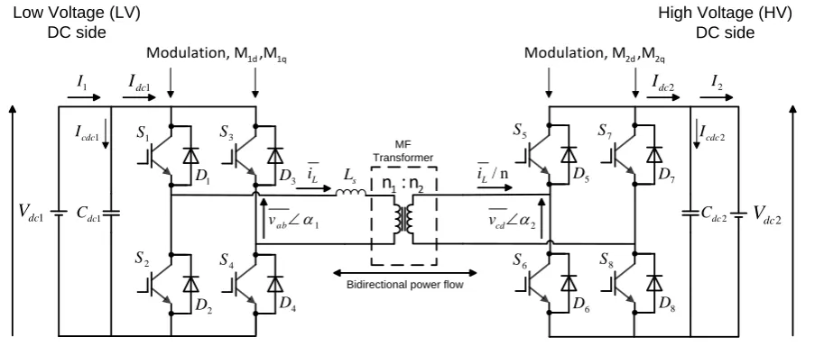
A single phase DAB DC/DC converter topology is shown in Fig. 1. It is assumed from this point that the power in the analysis is flowing in one direction (step up mode), from bridge 1 (LV) to bridge 2 (HV). The topology has one bridge working as a DC/AC converter feeding a MF transformer, which then supplies a second bridge working as an AC/DC converter. Each bridge is implemented by power switches S1-S4
(bridge 1) and S5-S8 (bridge 2). The power switches used are IGBT switches with anti-parallel diodes D1-D8.
Each bridge can be controlled using its PS angle to control the power flow and level. The AC equivalent circuit of the DAB converter inner circuit is shown in Fig. 2. The parameter Ls is the series inductance, iL is
2 1 n n : 1 S 2 S 3 S 4 S 5
S S7
6
S S8
1
D D3
4
D
2
D D6 D8
5
D D7
MF Transformer 1 dc I 1 ab v
L
i iL/ n
2
dc
I Low Voltage (LV)
DC side
High Voltage (HV) DC side 2 dc V 1 dc V
Bidirectional power flow
2
cd v
1
dc
C Cdc2
1d 1q
Modulation, M ,M Modulation, M ,M2d 2q
[image:5.595.71.533.53.245.2]s L 1 I 1 cdc I 2 I 2 cdc I
Fig. 1. DAB DC/DC converter topology
B. Circuit Equations
In the analysis, only the fundamental AC component of the square wave AC voltage is used (vab, vcd
variables in Fig. 1 is renamed to vac1, vac2 in Fig. 2, respectively). The transformer HV side parameters are
referred to the LV side. For simplicity, no losses are considered in the analysis. Also, the magnetizing inductance is assumed large enough to not affect the converter operation. The value of the magnetizing inductance is normally large and fixed depending on the core parameters such as its geometry and permeability. The aim of the analysis is focused on DC terminal fault based on the converter steady-state operation.
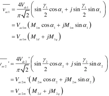
Referring to Fig. 2, the DAB converter instantaneous AC voltages can be expressed as phasors and its DQ coordinate form as
1 1 1 1 1
ac ac m ac d ac q
v V V jV (1)
2' 2 ' 2 2 ' 2 '
ac ac m ac d ac q
v V V jV (2)
where vac1, vac2' are the phasors of the AC voltages,
s L 2 1 n n : 2 ac v 2' ac v L i 1 ac v L i n
Fig. 2. DAB DC/DC converter AC equivalent circuit
α1, α2 are the phase shift angle (α1 is used as the reference coordinate frame),
Vac1d, Vac2d’ are the D component of the AC voltages, Vac1q, Vac2q’ are the Q component of the AC voltages.
Fig. 3 shows the basic operating waveforms of the DAB converter. From Fig. 3, α1 and α2 are the phase
angles of LV and HV sides, respectively. The conduction angles γ1 and γ2 are the modulation parameters to
control the AC voltage magnitudes. The control signals can also be separated into its DQ components and control parameters are introduced as M1d, M1q, M2d and M2q to link the phase angles, α1 and α2, and the
instantaneous AC voltage. Therefore, the RMS AC voltages are given as
1 1 1
1 1 1
1 1 1 1 1
1 1 1
4
sin cos sin sin
2 2
2
cos sin dc
ac
ac m m m
ac m d q
V
v j
V M jM
V M jM
(3)
2 2 2
2 2 2
2 2 2 2 2
2 2 2
4 '
' sin cos sin sin
2 2
2
' cos sin
' dc ac
ac m m m
ac m d q
V
v j
V M jM
V M jM
(4)
where γ1 and γ2 are the conduction angles of the switches which equals to M1m and M2m as the modulation
[image:6.595.40.225.422.584.2]t 1 2 ac
v
2
cdv
2 1 acv
abv
2 1
Fig. 3. Basic operating waveform of DAB
Then the steady-state equation for the RMS inductor current can be analyzed with the assumptions when bridge 1 is the referenced voltage (by setting α1 to zero). Therefore, the LV side AC voltage, vac1 in (1) equals Vac1m=Vac1d. The RMS inductor current can now be expressed as
1 ( 2 ' 2 ')
ac d ac d ac q L
s
V V jV
i
j L
(5)
where ω is the angular frequency of the converter.
The RMS inductor current can be expressed as its DQ components as
2 ' ( 2 ' 1 )
ac q ac d ac d
L Ld Lq Lm
s s
V V V
i j i ji i
L L
(6)
where iLd and iLq are the D and Q component of the inductor current, respectively. iLm is the magnitude of the
inductor current and θ is the inductor current angle.
Eq. (6) is used to calculate the apparent power of the converter at both bridges and can be expressed as
2
1 2 1 2 1
1 1
' ' '
' * ac d ac q ac d ac d ac d ac L
s s
V V V V V
S v i j
L L
2 2
1 2 1 2 2 2
2 2
' ' ' '
' * ac d ac q ac d ac d ac d ac q ac L
s s
V V V V V V
S v i j
L L
(8)
where the real part of (7) and (8) are the real power and the imaginary part are the reactive power. The negative sign in the real part indicate the power direction from LV to HV side and become positive for power transfer in the opposite direction.
Hence, the real power based on real part of (7) and (8) is assumed similar and can be used to calculate the required Ls such as
1 1 2 2 2
2
' sin( ) ac m m ac m m s
V M V M
L
P
(9)
The designed value of Ls in (9) determines the fault current magnitude of the converter. The DC fault
analysis is study in the following section.
III. DC FAULT ANALYSIS
The converter performance is investigated for DC terminal faults to derive the fault current magnitudes. Fig. 4 shows the AC equivalent of the DAB converter during LV and HV terminal faults. The DC fault depends on the power flow direction and on the location of the fault occurrence. This study assumes steady-state operation of the converter and no controller actions are realised.
As an example when there is no control action, the sequence of the DAB converter behaviour during LV side DC terminal fault is as follow:
2) During fault, the natural transient response of the uncontrolled diode bridge defines its performance until the converter achieves its steady state value.
3) The HV bridge sees this LV side fault current as AC faults and this fault current magnitude is primarily depends on the impedance of the converter.
s L
2 1 n
n :
2
ac
v
2'
ac
v
L
i
1 0
ac
v
/
L
i n
(a)
s L
2 1 n
n :
2 0
ac
v
2' 0
ac
v
L
i
1
ac
v
/
L
i n
[image:9.595.168.437.190.447.2](b)
Fig. 4. AC equivalent circuit of the DAB converter during (a) LV DC terminal fault, (b) HV DC terminal fault
On the other hand, similar sequence is expected when DC fault happened at HV side. The converter steady-state inductor current magnitude in (6) is used to investigate the fault current magnitude. The inductor current is at maximum when the converter is assumed to be operating at full power prior to fault (α2 is at 90˚).
During DC fault, the voltage across Ls only sees one voltage terminal is feeding the fault. At normal
operation, the resulting voltage across Ls sees two voltage terminals. This in turn gives higher voltage
magnitude across the Ls compared during DC fault. Hence, the inductor current during DC fault will always
A. DC fault current magnitude during LV fault
During LV DC side fault conditions (Fig. 4(a)), the DC voltage in (1) is rewritten to
1 1 1 0
ac ac m ac d
v V V (10)
From (6), the converter rated RMS inductor current magnitude during steady state operation is
2 ' ( 2 ' 1 )
ac q ac d ac d Lrm
s
V V V
i
L
(11)
Using (11), the magnitude of the LV fault current when substituting (10) gives
2 ' 2 '
ac d ac q LfmLV s V V I L
(12)
The magnitude ratio of (12) relative to (11) can be obtained using
2 2
_
2 2 1
' '
' ( ' )
ac d ac q Lfm LV
Lrm ac q ac d ac d
V V
I
I V V V
(13)
Rewriting (13) based on its control signals gives
2 2
2 2
_
2 2 2
2 2 1 2 1
2 2
2 2
2 2 2
2 2 1 2 1
' '
' ( ' 2 ' )
( 2 )
ac d ac q Lfm LV
Lrm ac q ac d ac d ac d ac d
d d
q d d d d
V V
I
I V V V V V
M M
M M M M M
(14)
Assuming maximum modulation and maximum phase shift angle of 90° (in this case M2d = 0, M2q = 1),
(14) is equal to
_ 1
2 Lfm LV
Lrm I
I (15)
_
2
2 Lrm
Lfm LVpk Lrm
I
I I (16)
The relationship between the steady-state and fault current based on (15) is given as
_ 0.707
Lfm LV Lrm
I I (17)
Eq. (17) is only valid if the converter is design to achieve its desired power level at maximum phase shift. If the converter is design say to achieve its desired power at 45° (designing and operating at smaller phase shift angle can reduced the circulating current in DAB converter), (17) becomes ILfm_LV = 1.31ILrm. This is
bigger than the rated current value.
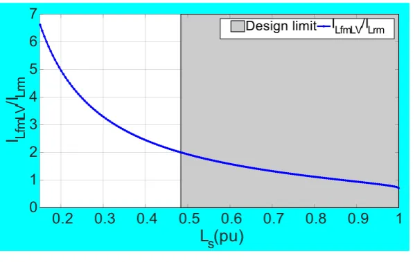
Therefore, it is required to set the boundary when the converter fault current exceeds its rated current value. The boundary ratio in (14) is set to two (ILfm_LV = 2ILrm). The reason for selecting the limit at two
times the rated current is because the power switches can withstand double of its rated value during transient operation which can be happened at the instant DC fault occur [15-16]. However, this operation is limited to the junction temperature of the power switches. The boundary of the converter design of Ls is based on per
[image:11.595.157.457.496.685.2]unit (pu) value. Fig. 5 shows the fault and rated current magnitude ratio calculated using (14) against different series inductance per unit value.
The DAB converter series inductance, Ls boundary within the limit set and the operating phase shift
angle to achieve a desired power are
2
0.48 1.0
28.96 90 s L
pu pu
(18)
The boundary of α2 is calculated using (14) by rewriting the equations based on its sine and cosine
functions.
B. DC fault current magnitude during HV fault
On the other hand, during HV side fault (as shown in Fig. 4(b)), the HV DC terminal voltage in (2) becomes
2' 2 ' 0
ac ac m
v V (19)
Using (11), the magnitude of the AC fault current when substituting (19) is
1 _
ac d Lfm HV
s V I
L
(20)
The magnitude ratio of (20) relative to (11) is
_ 1
2 ' ( 2 ' 1 )
Lfm HV ac d
Lrm ac q ac d ac d
I V
I V V V (21)
And rewriting (21) to its control signals gives
2
_ 1 1
2 2 2 2
2 1 2 1
( ') ( )
Lfm HV ac d d
Lrm ac q ac d q d
I V M
I V V M M
(22)
similar for both HV and LV sides. The only difference is because of the transformer turns ratio. The following section shows the plots facilitated using MATLAB for the LV and HV side DC fault studies.
C. DC fault MATLAB plots
The DAB converter specification used for the study is given in Table I. The AC fundamental component analysis in this paper is compare with the piecewise linear analysis such as in [8] to determine its accuracy. The power equation in [8] is
1 2
2 (1 )
dc dc lit
V nV P
L
(23)
where Vdc1, Vdc2 are the voltages at DC terminals, n is the transformer turns ratio, φ is the phase shift
angle in radian, L is the inductance, P2lit is the required output power and ω = 2πf where f is the converter
operating frequency.
The inductance for this comparison can be calculated based on (9) for fundamental component analysis and based on (23) for piecewise linear analysis. The calculation of the inductance is using the maximum phase shift angle of 90°. The difference between the two powers is minimal as depicted in Fig. 6 which validate the analysis based on AC fundamental component. P2lit is compared with real part of (7) or (8), P2
with varying phase shift angle, α2 to show the whole range of power level.
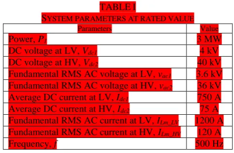
TABLE I
SYSTEM PARAMETERS AT RATED VALUE
Parameters Value
Power, P1 3 MW
DC voltage at LV, Vdc1 4 kV
DC voltage at HV, Vdc2 40 kV
Fundamental RMS AC voltage at LV, vac1 3.6 kV
Fundamental RMS AC voltage at HV, vac2 36 kV
Average DC current at LV, Idc1 750 A
Average DC current at HV, Idc2 75 A
Fundamental RMS AC current at LV, ILm_LV 1200 A
Fundamental RMS AC current at HV, ILm_HV 120 A
[image:13.595.178.420.370.528.2]-90 -60 -30 0 30 60 90 -3
-2 -1 0 1 2 3
2(deg)
P 2
(M
W
)
P
2
P
[image:14.595.147.444.60.208.2]2lit
Fig. 6. Comparison of the power level using fundamental component analysis and literature [8]
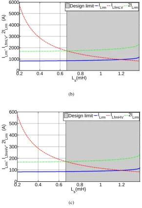
Fig. 7 shows the rated and fault current RMS magnitude for fault at LV and HV side terminals using (12) and (20), respectively. The design limit of two times the rated current is also included in Fig. 7 to give the design boundary for the DAB converter. The per unit plot is given in Fig. 7(a) where the value of Ls (pu)
that the fault current magnitude exceeds the rated pu current magnitude is 0.866 pu while the set boundary of two times the rated pu current 0.48 pu. Below the set boundary limit, the fault current can significantly increase if no controller is realised. Based on the specification in Table I, the value of Ls that the fault
current magnitude exceeds the rated current magnitude is 1.19 mH while the set boundary of two times the rated current magnitude is 0.67 mH for the LV and HV sides DC terminal fault are shown in Fig. 7(b) and Fig. 7(c), respectively.
0.2 0.3 0.4 0.5 0.6 0.7 0.8 0.9 1
0 1 2 3 4 5 6 7
L s(pu)
I Lrm , I L
fm
L
V
,
2
I Lrm
(p
u
)
Design limit ILrm ILfmLV 2ILrm
[image:14.595.145.454.510.707.2]0.20 0.4 0.6 0.8 1 1.2 1000
2000 3000 4000 5000 6000
L
s(mH)
I Lrm , I L
fm
L
V
,
2
I Lrm
(A)
Design limit ILrm ILfmLV 2ILrm
(b)
0.20 0.4 0.6 0.8 1 1.2
100 200 300 400 500 600
Ls(mH)
I Lrm , I L
fm
H
V
,
2
I Lrm
(A)
Design limit ILrm ILfmHV 2ILrm
[image:15.595.151.443.63.492.2](c)
Fig. 7. Rated and fault current RMS magnitude, (a) per unit value (b) LV side DC terminal fault (using Table I), (c) HV side DC terminal fault (using Table I)
IV. SIMULATION RESULTS
= 0.1 second. Prior to fault, the converter is also assumed to be operating at full power and the power flow is from LV to HV side.
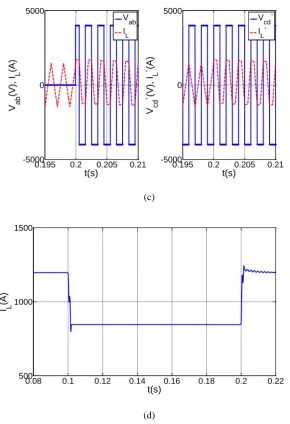
In Fig. 8, the AC voltages, vab, vcd and inductor current, iL are shown for the case of LV side faults
(Vdc1=0). For the LV side, the actual simulated values are shown while for the HV sides, all the variables are
referred to the LV side values. iL is shown on for convenient to observed the waveform on LV and HV
sides, but this value is similar. Zoom view of the AC voltages and inductor current during fault and after fault are given for better observations of the converter performance during fault. The RMS inductor current during steady state is approximately 1200 A. During fault, the RMS inductor current magnitude is 850 A. This value agrees with (17) which confirm that the converter is operating at lower RMS current during DC fault. Triangular waveform has smaller RMS value compare to sinusoidal and trapezoidal waveforms. The peak can also be observed from the zoom view to be similar as the steady state value.
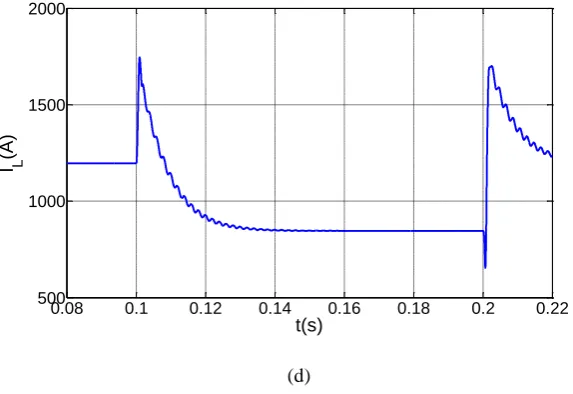
During fault at HV (Vdc2 = 0), the AC sides voltages and currents waveforms are shown in Fig. 9. In Fig.
9(b), the RMS fault current magnitude is observed to be at 850 A (similar to LV side fault because this is referred value). At the instant DC fault is applied, transient peak current is observed at 40% more than the steady-state current. Comparing to (22), the magnitude ratio of the fault current is observed to be 1.4 times more than the steady-state current. For this specific simulation, the overshoot is caused by the voltage across inductor (vL = vab-vcd’) is high compare to fault at LV sides. This transient peak current gives non-zero
Both DC fault cases have RMS fault current magnitude shown in Fig. 8(d) and 9(d) shows similarity to the theoretical study value as depicted in Fig. 7. The converter shows good response when DC fault is applied and during fault recovery without any control actions. The performance of the DAB converter for reverse power (from HV to LV sides) is expected to be similar.
0.08 0.1 0.12 0.14 0.16 0.18 0.2 0.22 -5000
0 5000
t(s)
V a
b
(V),
I L
(A) Vab
IL
0.08 0.1 0.12 0.14 0.16 0.18 0.2 0.22 -5000
0 5000
t(s)
V c
d
`(V),
I L
`(A) Vcd`
IL`
(a)
0.095 0.1 0.105 0.11 -5000
0 5000
t(s)
V a
b
(V),
I L
(A)
Vab IL
0.095 0.1 0.105 0.11 -5000
0 5000
t(s)
V c
d
`(V),
I L
`(A)
Vcd` IL`
0.195 0.2 0.205 0.21 -5000
0 5000
t(s)
V a
b
(V),
I L
(A)
Vab IL
0.195 0.2 0.205 0.21 -5000
0 5000
t(s)
V c
d
`(V),
I L
`(A)
Vcd` IL`
(c)
0.08 0.1 0.12 0.14 0.16 0.18 0.2 0.22 500
1000 1500
t(s)
I L
(A)
[image:18.595.148.439.57.482.2](d)
0.08 0.1 0.12 0.14 0.16 0.18 0.2 0.22 -5000 0 5000 t(s) V a b (V), I L
(A) Vab
IL
0.08 0.1 0.12 0.14 0.16 0.18 0.2 0.22 -5000 0 5000 t(s) V c d `(V), I L
`(A) Vcd`
IL`
(a)
0.095 0.1 0.105 0.11 -5000 0 5000 t(s) V a b (V), I L (A) Vab IL
0.095 0.1 0.105 0.11 -5000 0 5000 t(s) V c d `(V), I L `(A)
Vcd` IL`
(b)
0.195 0.2 0.205 0.21 -5000 0 5000 t(s) V a b (V), I L (A) Vab IL
0.195 0.2 0.205 0.21 -5000 0 5000 t(s) V c d `(V), I L `(A)
Vcd` IL`
0.08 0.1 0.12 0.14 0.16 0.18 0.2 0.22 500
1000 1500 2000
t(s)
I L
(A)
[image:20.595.148.435.63.260.2](d)
Fig. 9. Time domain simulation fault at HV DC terminal, (a) AC voltages and currents, (b) Zoom view during fault is applied, (c) Zoom view during fault recovery, (d) fundamental RMS inductor current magnitude
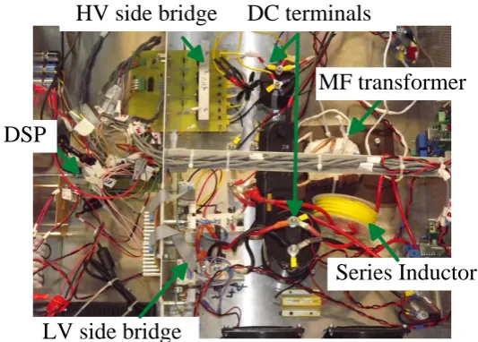
V. PROTOTYPE
HV side bridge DC terminals
MF transformer
DSP
Series Inductor
[image:21.595.164.431.56.247.2]LV side bridge
Fig. 10. 500 W prototype of the DAB DC/DC converter
Fig. 11 shows typical DAB converter waveform during steady-state operation. In this figure, the yellow waveform is the LV AC voltage, vab, the green waveform is the AC voltage at HV side, vcd, the blue and red
waveform is the inductor current (blue waveform are taken from the LV side and red waveform from the HV side).
TABLE II
SYSTEM PARAMETERS AT RATED VALUE
Parameters Value
Power, P1 500 W
DC voltage at LV, Vdc1 24 V
DC voltage at HV, Vdc2 100 V
Average DC current at LV, Idc1 20.83 A
Average DC current at HV, Idc2 5 A
Frequency, f 2000 Hz
[image:21.595.167.454.423.584.2]ab v
cd v
L i
n
L i
Fig. 11. Steady-state AC voltages and currents waveforms during normal conditions
DC terminal fault is tested experimentally to verify the DAB converter capability and performance during fault. A DC fault hardware circuit is connected across the LV DC terminal. It is consists of power semiconductor device and power resistors used to short and direct fault current, respectively. DC fault is applied for 0.9 ms before fault recovery. Only DC fault at LV side is tested and enough to confirm the theoretical work. The waveform in Fig. 12 shows the LV side DC fault. The yellow waveform is the LV DC terminal voltage, Vdc1, the green waveform is the AC voltage at LV side, vab, the blue waveform is the
inductor current, iL and the red line is the DC current at LV side, Idc1. During fault is applied, the converter
performance is as expected (similar behaviour as simulation). No damaging current is observed. The peak value is also similar as analysed theoretically and as observed during simulations work. It can also be seen that the current waveform becomes triangular during fault. The peak current before and during DC fault has similar peak magnitude as expected. It is observed that the AC voltage, vab in Fig. 12(a) is non zero whereas
in Fig. 8(a), vab is zero. This non zero voltage is the voltage across the design value of the fault hardware
1
dc V
ab v
L i
1
dc i
(a)
1
dc V
ab v
L i
1
dc i
1
dc V
ab v
L i
1
dc i
[image:24.595.131.464.56.265.2](c)
Fig. 12. Practical results for the DAB 500 W prototype, (a) LV DC terminal fault for the, (b) During DC fault is apply (c) Recovery after DC fault
At the DC side current, a transient peak is observed during fault but this is within the capability of the switches transient (pulse current) specification. The fault recovery is as expected and it takes less than 100 μs for the converter to recover to its normal steady-state operation.
VI. CONCLUSION
This paper has introduced fault studies for DAB DC/DC converter based on its fundamental component of the AC voltages and currents. The fault currents were derived and simulated for DC terminal fault using MATLAB/Simulink. The performance of the converter was satisfactory during DC fault operation. The theoretical fault study has been confirmed by simulation and experimental works. This study concluded that the converter is capable to operate during faults even without any control action.
REFERENCES
[2] C. Meyer, M. Kowal and R.W. De Doncker, “Circuit breaker concepts for future high-power DC distribution systems,” Proc. 2005 IEEE Ind. App. Society, vol. 2, pp. 860-866.
[3] M.E. Baran and N.R. Mahajan, “Overcurrent protection on voltage source converter-based multiterminal DC distribution systems,” IEEE Trans. Power Delivery, vol. 22, no. 1, pp. 406-412, Jan. 2007.
[4] J. Hafner and B, Jacobson, “Proactive Hybrid HVDC Breakers - A key innovation for reliable HVDC grids,” Proc. CIGRE 2011 Bologna Symposium, Bologna, Italy, paper 264.
[5] M. Hajian, D. Jovcic and B. Wu, “Evaluation of Semiconductor Based Methods for Fault Isolation on High Voltage DC Grids,” IEEE Trans. Smart Grids, vol. 4, no. 2, pp. 1171-1179, June 2003.
[6] P.M McEwan and S.B. Tennakoon, “A two-stage DC thyristor circuit breaker,” IEEE Trans. Power Electronics, vol. 12, no. 4, pp. 597-607, July 1997.
[7] F. Deng and Z. Chen, “Design of protective inductors for HVDC Transmission Line within DC Grid Offshore Windfarms,” IEEE. Trans. Power Delivery, vol. 28, no. 1, pp. 75-83, Jan. 2013.
[8] M.H. Kheraluwala, R.W. Gascoigne, D.M. Divan and E.D. Baumann, “Performance characterization of a high power dual active bridge dc-to-dc converter,” IEEE Trans. Ind. Applicat., vol. 28, pp. 1294-1301, Nov. 1992.
[9] S. Han, I. Munuswamy and D. Divan, “Preventing transformer saturation in bi-directional dual active bridge buck-boost DC/DC converters,” Energy Conversion Congress and Exposition (ECCE 2010), pp.1450-1457.
[10] E. Ribeiro, A.J. Marques Cardoso, C. Boccaletti, “Fault analysis of dual active bridge converters,” in
Proc. 2012 IEEE 38th Ind. Electron. Conf. (IECON 2012), pp. 398-408.
[12] X. Pei, S. Nie, Y. Chen, and Y. Kang, "Open-Circuit Fault Diagnosis and Fault-Tolerant Strategies for Full-Bridge DC-DC Converters, " IEEE Transactions on Power Electron., vol. 27, no. 5, pp. 2550-2565, May 2012.
[13] L. Tang and B.T Ooi, “Locating and Isolating DC Faults in Multi-Terminal DC Systems,” IEEE Trans. Power Delivery, vol. 22, no. 3, pp. 1877-1884, Jul. 2007.
[14] D. Jovcic and J. Zhang, “High power IGBT-based DC/DC converter with DC fault tolerance”, Proc. 2012 IEEE Power Electron. and Motion Control Conf., Novi Sad, Serbia, 2012.
[15] D. Jovcic, L. Zhang, and Masood Hajian, “LCL VSC Converter for High-Power Applications”, IEEE Trans. Power Delivery, vol. 28, no. 1, pp. 137-144, Dec. 2012.

![Fig. 6. Comparison of the power level using fundamental component analysis and literature [8]](https://thumb-us.123doks.com/thumbv2/123dok_us/1408387.93751/14.595.147.444.60.208/comparison-power-level-using-fundamental-component-analysis-literature.webp)